Magnetization dependent current rectification in (Ga,Mn)As magnetic tunnel junctions
Abstract
We have found that the current rectification effect in triple layer (double barrier) (Ga,Mn)As magnetic tunnel junctions strongly depends on the magnetization alignment. The direction as well as the amplitude of the rectification changes with the alignment, which can be switched by bi-directional spin-injection with very small threshold currents. A possible origin of the rectification is energy dependence of the density of states around the Fermi level. Tunneling density of states in (Ga,Mn)As shows characteristic dip around zero-bias indicating formation of correlation gap, the asymmetry of which would be a potential source of the energy dependent density of states.
pacs:
75.50.Pp, 85.75.Mm, 75.76.+jControl of device characteristics through spin-degree of freedom is one of the expected novel functionalities in semiconductor spintronics. In metallic magnetic tunnel junctions (MTJs), rectification of microwaves driven by ferromagnetic resonance (FMR) has been reported Tulapurkar2005 . This arises interests in the effect of ferromagnetism on the rectification properties in diluted magnetic semiconductor (DMS) devices. In strongly asymmetric structures such as Schottky or p-n junctions, the rectification is naturally realized through steep electrostatic band-bending, which cannot be expected in unipolar MTJs ordinarily obtained in DMSs. For example in the case of (Ga,Mn)AsOhno1996 , the material should be p-type for the appearance of the ferromagnetismKomori2003 , which is mediated by charge carrying holes. Instead spin-polarization may thus be utilized to commutate alternative currents. In this letter, we report such rectification effect in (Ga,Mn)As tri-layer MTJs, in which very small threshold current for spin-injection magnetization reversal Watanabe2008 . The rectification is sensitive to the alignment of the magnetizations and hence can be controlled through bi-directional current injection.
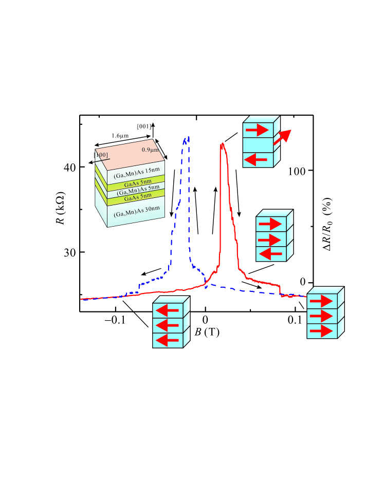
The inset of Fig.1 schematically shows the cross section of the layered structure grown by standard low temperature molecular beam epitaxy (LTMBE) onto a (001) p+(Zn-doped) GaAs substrateShen1997 with the growth temperature of 320C. The middle “free” layer is designed to be thinner than the other two to have smaller coercive force, which turned out to be, in reality, comparable to that of the top layer as we will see later. The ferromagnetic transition temperature estimated from the appearance of hysteretic tunneling magnetoresistance (TMR) is about 40K. With use of electron beam lithography, the film was wet-etched into mesas with 1.40.9 rectangles along [100], which is an easy axis of the in-plane magnetization though the anisotropy should be weakened through the stress relaxationSuda2010 . Each device was attached to a coplanar waveguide (CPW) with [100] parallel to the external magnetic field. Here the doped substrate is electrically bonded to the center strip and separately ordinal wires for DC are connected. The AC and DC lines were cut by bias tees. Due to the high impedance of the devices, the AC sources drove the device voltages and the rectified currents were measured through a current-voltage amplifier or calculated from the DC voltages along the device and the I-V characteristics. The external magnetic field of 0.7T was applied along [100] during cooling from room temperature to 4.2K.
Figure 1 shows a typical TMR for a major magnetic field loop. The lineshape resembles to those reported so far Watanabe2008 , suggesting similarity in magnetization alignments, of which a possible set are illustrated for typical values of magnetic field. Actually there should be several variations in the alignment around those simplified ones as can be seen in small step structures. This is probably due to the reduction in the in-plane crystallographic anisotropy through relaxation of biaxial strain with micro-fabricationSuda2010 .
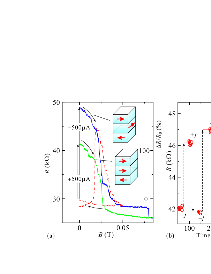
Note that smallest coercive force is assumed in the the top layer in the illustrated alignments in order for natural interpretation of the response to current injection. This clearly appears in the response to the spin injection by current pulses. A sequence consists of a minor field loop 0T 0.06T 0T and a current injection at zero field is adopted in Fig.2(a). As shown in Fig.2(a), the junction resistance jumps up to the branch of the highest resistance when the electric current of 500A flows from the substrate to the upper electrode (we define this direction as ‘negative’ current). The pulse width can be as short as 3ms, which is limited by wiring in the cryostat. A resistance leap with smaller increment is observed also for positive current pulse. To assign these states of resistance to the alignments of magnetization, we need to assume
The switching between these two is reversible, i.e., as shown in Fig.2(b), the state flip-flops between them with alternating current injections, which can be explained with assuming conditions as 90 degree rotation of the free layer with injected spin torques.
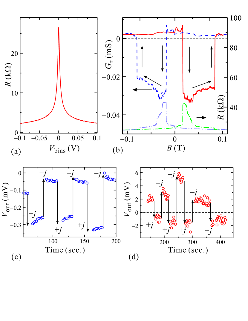
The current-voltage (I-V) characteristics were strongly non-linear, that is, the differential resistance is reduced with the source-drain voltage as shown in Fig.3(a). When the junction is driven by an AC voltage, time-averaged resistance is hence reduced, and this can be utilized for estimation of the AC amplitude. We here eliminated the possibility of heating under the AC voltages by measuring the TMR and hence the magnetic coercive force, which is found to be sensitive to the temperature. A kind of conductance, (rectified DC current)/(AC drive voltage amplitude), can therefore serve as a measure of the rectification.
In spite of the almost symmetric I-V characteristics, a clear rectification voltage appears with the application of AC voltages. Figure 3(a) shows as a function of external magnetic field at the AC frequency of 1.4GHz. has a small positive value for parallel alignments and large negative outputs appear for alignments with anti-parallel or perpendicular junctions. Clear correspondence between and the TMR is observed though it is not monotonic. Because is sensitive to the magnetization alignment, it also can be controlled with spin-injection. Figure 3(b) displays flip-flop switching of the rectification conductance. The conditions can also be tuned so that the direction of the rectification can be switched with spin-injection. Figure 3(c) demonstrates such reversal of rectification direction by current (spin) injection at zero field in another device.
Henceforth we discuss possible origin of the rectification. The fact that the sign of output changes with the configuration of magnetization eliminates the possibility that the source is zero-point shift in the I-V characteristics due to some imbalance in the circuit including thermoelectric voltages in cryogenic wires, which only modifies the amplitude. We have measured frequency dependence of from 1GHz to 8GHz (the limit of our microwave source) and found it very weak. The spin torque diode effect is ruled out because it is based on FMR and thus should have strong frequency dependence.
We look for a possible explanation in the simplest model of magnetic tunnel junctions (MTJs) by JulliereJulliere , in which the conductance of an MTJ is a function of the majority and minority subbands density of states in the electrodes. A slight modification here is energy () and electrode () dependent density of states and for the majority and the minority spin subbands respectively. We take the Fermi energy as zero and the current differences for voltages are proportional to sum of convolutions as
| (1) | ||||
| (2) |
for anti-parallel and parallel configurations respectively.
It is apparent from (1), (2) that rectification stems from the above mechanism only when the density of states are asymmetric to and also between the electrodes. In MTJ’s with metal ferromagnets constant density of states approximation usually holds around and the rectification does not appear.
To check whether the density of states in (Ga,Mn)As has such energy dependence, we prepared a tunnel junction, which connects (Ga,Mn)As and p+-GaAs layers with a single AlGaAs barrier layer (the inset of Fig.4(a)). The film was cut into a 1010 (m)2 mesa and two metal electrodes were placed both on the top and the bottom layers for four wire measurement.
Figure 4(b) shows the differential conductance of the junction as a function of bias voltage in four wire measurement. At the origin we observe a dip structure, which can be expressed as . This probably due to so called Efros-Shklovskii (ES) gap, which originates from electron-electron configuration interaction in disordered insulators. The ES gap manifests that the hole states in (Ga,Mn)As is close to those in disordered insulators rather than those in degenerate semiconductors. However the gap cannot be the direct origin of the rectification because of the parabolic energy dependence around , which is symmetric to . Besides the gap structure we find significant asymmetry to zero-bias, which can cause the rectification in combination with the difference between layers due to that in the thicknesses, etc. Such asymmetry is more natural for the impurity band model than the degenerate semiconductor.
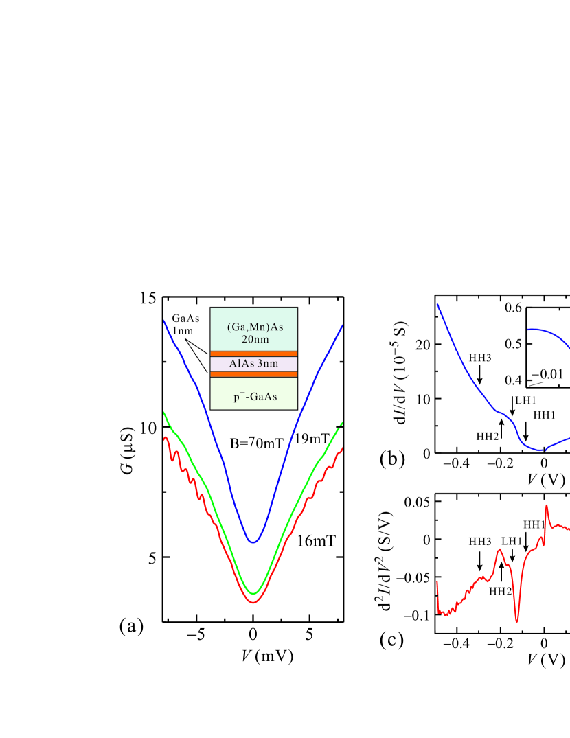
Attention must be paid also to characteristic peaks and shoulders in negative bias. These can be interpreted as the result of quantum confinement in the (Ga,Mn)As layer, which is put between the internal (Al,Ga)As layer and the surface Schottky barrierOhya2007 . The voltage derivative of differential conductance is shown with a possible quantized level assignment is shown in Fig.4(b). For the assignment, we assume the effective thickness of the (Ga,Mn)As as 8nm, namely the Schottky depletion width as 12nm. The triangular potential with 12nm width and 0.5eV height gives 300 /(m)2 for the contact resistance, which is in reasonable agreement with that estimated from the difference between the two-wire and the four-wire resistances (300-800 /(m)2). The result indicates that while the impurity band states are nearly localized, the valence band of matrix GaAs is kept comparatively ordered and coherent. Also the result suggests the possibility of designing the rectifying characteristics because these anomalies can be controlled through the thicknesses of the constituent layers.
In summary, we have found current rectification effect in tri-layer (Ga,Mn)As MTJs for AC voltages up to 8GHz. The rectification is strongly dependent on the alignment of the magnetizations and can be reproducibly switched by using current injection with very low threshold at zero field. We have shown that the asymmetry of the density of states at the Fermi energy is a possible origin of the rectification.
This work was supported by Grant-in-Aid for Scientific Research and Special Coordination Funds for Promoting Science and Technology.
References
- (1) A. A. Tulapurkar, Y. Suzuki, A. Fukushima, H. Kubota, H. Maehara, K. Tsunekawa, D. D. Djayaprawira, N. Watanabe, and S. Yuasa: Nature 438 (2005) 339.
- (2) H. Ohno, A. Shen, F. Matsukura, A. Oiwa, A. Endo, S. Katsumoto, and Y. Iye: Appl. Phys. Lett. 69 (1996) 363.
- (3) T. Komori, T. Ishikawa, T. Kuroda, J. Yoshino, F. Minami, and S. Koshihara:
- (4) M. Watanabe, J. Okabayashi, H. Toyao, T. Yamaguchi, and J. Yoshino: Appl. Phys. Lett. 92 (2008) 262.
- (5) A. Shen, and H. Ohno, F. Matsukura, Y. Sugawara, N. Akiba, T. Kuroiwa, A. Oiwa, A. Endo, S. Katsumoto, and Y. Iye: J. Crys. Growth. 175 (1997) 1069.
- (6) K. Suda, S. Kobayashi, J. Aoyama, and H. Munekata: IEEE trans. Magnetics 6 (2010) 2421.
- (7) M. Julliere: Phys. Lett. A 54 (1975) 225.
- (8) S. Ohya, K. Tkata, I. Muneta, P. N. Hai, and M. Tanaka: arXiv:1009.2235. Phys. Rev. B 67 (2003) 115203.