Substrate gating of contact resistance in graphene transistors
Abstract
Metal contacts have been identified to be a key technological bottleneck for the realization of viable graphene electronics. Recently, it was observed that for structures that possess both a top and a bottom gate, the electron-hole conductance asymmetry can be modulated by the bottom gate. In this letter, we explain this observation by postulating the presence of an effective thin interfacial dielectric layer between the metal contact and the underlying graphene. Electrical results from quantum transport calculations accounting for this modified electrostatics corroborate well with the experimentally measured contact resistances. Our study indicates that the engineering of metal-graphene interface is a crucial step towards reducing the contact resistance for high performance graphene transistors.
Since its experimental isolation novoselov01 ; novoselov02 ; zhang01 , graphene has attracted significant attention from the scientific community, due to its unique electronic structure and physical properties geim01 ; neto09 . Its excellent transport properties and the ability to tune the carrier concentration with electrical gates, also makes it a material with great technological promise. Potential applications range from RF devices and transistors avouris01 ; lin10 ; schwierz01 to bio-sensors schedin07 and flexible electronics kim08 . The metal-graphene contact, is however, a key technological challenge for graphene-based electronic devices. For current-generation silicon metal-oxide-semiconductor field-effect transistors (MOSFETs), the International Technology Roadmap for Semiconductors calls for a resistance of - per contact, which is about 10% of the transistor’s on-resistance roadmap01 . Graphene’s excellent transport properties should produce transistor on-resistances considerably lower than those of silicon MOSFETs. To realize the performance potential afforded by the excellent transport properties of graphene, exceptionally low contact resistances will be required schwierz01 ; avouris01 . It is, therefore, essential to develop a thorough understanding of metal-graphene contacts and of the fundamental lower limits for the contact resistance. In this paper, we develop a model that explains the recently observed substrate modulation of contact resistance in graphene transistors chen01 ; kim02 . We argue that this effect is due to the presence of an effective thin metal-graphene interfacial dielectric layer. Using this model, we estimate two important components of the series resistance and establish lower bounds for the contact resistance. The study provides an improved understanding of the metal-graphene contact that may prove useful for improving device performance.
Graphene is sensitive to external perturbations due to its all-surface and zero volume nature schedin07 . Charge transfer between metal and graphene due to a workfunction difference dopes the underlying graphene giovannetti01 . Contacts, therefore, introduce a built-in electrostatic junction within graphene, which was observed experimentally using scanning tunneling microscopy zhao01 . A distinct experimental signature was the asymmetry of resistance in back-gated devices huard01 ; cayssol01 . The sign of this asymmetry reflects the doping of the graphene underneath the metal. Recently, devices with top and bottom gating schemes, as shown in Fig. 1, were experimentally realized chen01 ; kim02 . Measurement of resistance vs. top gate voltage () revealed an asymmetry, whose sign and magnitude were modulated by the back gate voltage (). This observation strongly suggests that the graphene doping underneath the metal was substantially modulated by the back gate voltage.
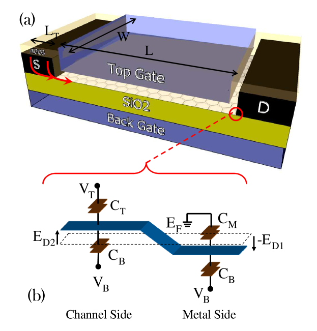
It is instructive to recall that in standard metal-semiconductor junction theory, the Schottky barrier height is given by the difference between the metal workfunction, , and the electron affinity, , of the semiconductor, when there is no Fermi level pinning. However, the metal-graphene binding is comparatively weaker. The nature of the interfacial metal-graphene chemical bonding is still a subject of theoretical study vanin01 . Electrically, this interfacial layer can be modelled with an interfacial capacitance . If and , where stands for the density-of-states, then one expects the Dirac point of graphene to be stationary with respect to . The above limit describes the standard metal-semiconductor junction, since is generally significantly larger than the semiconductor capacitance. If , it is possible to modulate with an applied voltage . Consideration of this fact is key to explaining the experimental results chen01 of the device shown in Fig. 1.
The model: From Gauss’s law, the electrostatic equations governing the graphene underneath the contact (region ) and top gate (region ) are
| (1) | |||
| (2) |
where is the workfunction difference between metal and graphene, and . Note that is taken to be zero as reference. The transition between region and is described by an analytical screening model zhang02 , assuming a linear graded junction. The junction resistance, , is then computed quantum mechanically using a previously developed mode space non-equilibrium Green function method for graphene Low01 . For our ballistic study, the effect of temperature impacts our results only through the thermal smearing due to Fermi-Dirac distribution function, which is included in our study.
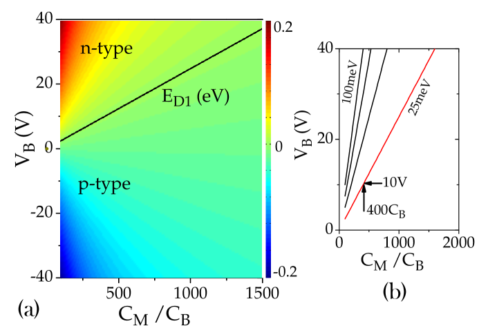
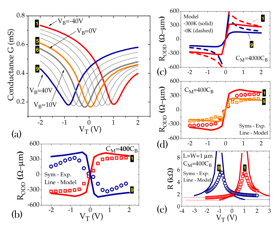
In the experiment chen01 , the gate capacitances are known, i.e. and . On the other hand, is a quantity to be determined. Ti/Pd/Au is used for the metal contacts. For our calculations, we assumed , a value that is sensible for our experimental metal stack 111Literature on metal workfunction on graphene reports wide range of , suggesting that experimental condition and surface physics introduce variability. Experiments have provided indication about the metal-graphene function difference, based on quantitative analysis huard01 , and photocurrent study mueller01 . From a computational standpoint, DFT studies giovannetti01 ; vanin01 ; giovannetti01 have provided support for a spectrum of work function differences in a range for several different metal compositions.. Fig. 2a plots as a function of and . As expected, modulates the doping in region , with greater ease when is smaller. In the experiments, it was observed that the conductance as function of exhibits the least asymmetry when (see Fig. 3a). This suggests that when , (the charge neutrality point), which then also allows us to pin down to be . On the other hand, a different choice of would correspondingly yield a different , as illustrated in Fig. 2b.
Results: The measured conductance, , for different values of is shown in Fig. 3a. The observed asymmetry in changes sign at about . To facilitate comparison between experiment and a ballistic theory, we extract the odd component of the resistance huard02 from experiment, given by , where is with respect to the Dirac point voltage. The quantity then allows for quantitative comparison between the experimentally measured and the numerically calculated . Although interface charge, moisture, and chemicals in the vicinity may impact the transport properties of the graphene devices, these effects can be minimized by careful control of the fabrication process and the measurement conditions so that any asymmetry can be attributed entirely to the graphene p-n junction.
.
In Fig. 3b, the striking experimental observation of asymmetry inversion, as it is observed in vs and , is compared with our modeled for a work function difference and an interfacial capacitance . As elucidated previously, modulation of the doping of graphene underneath the metal is possible because is not large enough to completely dominate over . In fact, for a moderate carrier concentration of , one obtains . If one assumes that the metal-graphene interfacial layer is an air gap, would then translate to a physical thickness of only . This is in good agreement with recent density functional studies boukhvalov01 , with a predicted metal-graphene binding distance of . The possibility of sign inversion is, however, conditional. For example, if we use a value of instead of , sign inversion of would not be observed within the range of interest, as shown in Fig. 3c. In Fig. 3d, we show that the increasing odd resistance with increasing , as it is observed in the experiment for , can also be captured with our simulation, using .
Up till now, we only considered and its contribution to the asymmetric part of the contact resistance. Previous studies chen02 ; perebeinos01 of the intrinsic transport properties of graphene on substrate allow one to make reasonable estimates of the channel resistance, , by including contributions due to acoustic/optical phonons and substrate-induced remote phonons. However, their contributions relative to are not as significant 222For example, acoustic phonons limited resistivity is only at room-temperature chen02 . Since our device has an aspect ratio of . This contribution is not significant compared to . . A modest mobility of was extracted from the experiment in vicinity of the Dirac point, suggesting high levels of impurities adam07 . Here, we model the impurity limited resistivity with the Laudauer formula using a mean-free-path proportional in energy i.e. , where is used to fit the mobility and is the number of modes normalized to . In Fig. 3e, we compare the experimental resistance with the calculated sum . By construction, our model does not capture the physics at the Dirac point. However, far away from the Dirac point, one observes an unaccounted for excess resistance in the experiment of , the origin of which is the subject of subsequent discussion.
Other contributions to contact resistance include the current crowding effects due to access geometry and the presence of the metal-graphene interfacial layer. The latter implies that current has to tunnel across a dielectric layer, encapsulated in the electrical quantity . The tunneling resistivity can be estimated using a model for quasi-bound electrons leggett01 , commonly used in the study of gate leakage current in semiconductor inversion layers hou01 . It is given by , where is the Wentzel Kramers Brillouin tunneling probability estimated to be , and is known as the classical bounce time leggett01 , which in graphene is simply , with and being the thickness of graphene and Fermi velocity respectively. Here, we take to be the carbon-carbon bond length, . This yields us a tunneling resistance estimate of - for a pair of contacts. This value is reasonably close to a recently reported nagashio02 experimental value of -.
Expanding the prior analysis to the spatial distribution of carrier flow, the current crowding effects due to the metal-graphene acesss geometry lead to an effective electrical area for the contact where current flows, given simply by , where is commonly known as the transfer length. With and , we denote the specific contact resistivity and the sheet resistance of the graphene layer underneath, respectively. Using our estimated - and a sheet resistance from the experiment chen01 , at a channel carrier concentration , we find . Given the experiment to experiment variations in and , this value is within a reasonable range nagashio02 .
Perspective: Recently reported contact resistance values lie in the range - blake01 ; kim02 ; nagashio02 ; russo01 ; venugopal01 ; liu10 (see Suppl. Info.). These values are considerably above what is required for high performance transistors roadmap01 . In this section, we examine several issues related to the fundamental limit to .
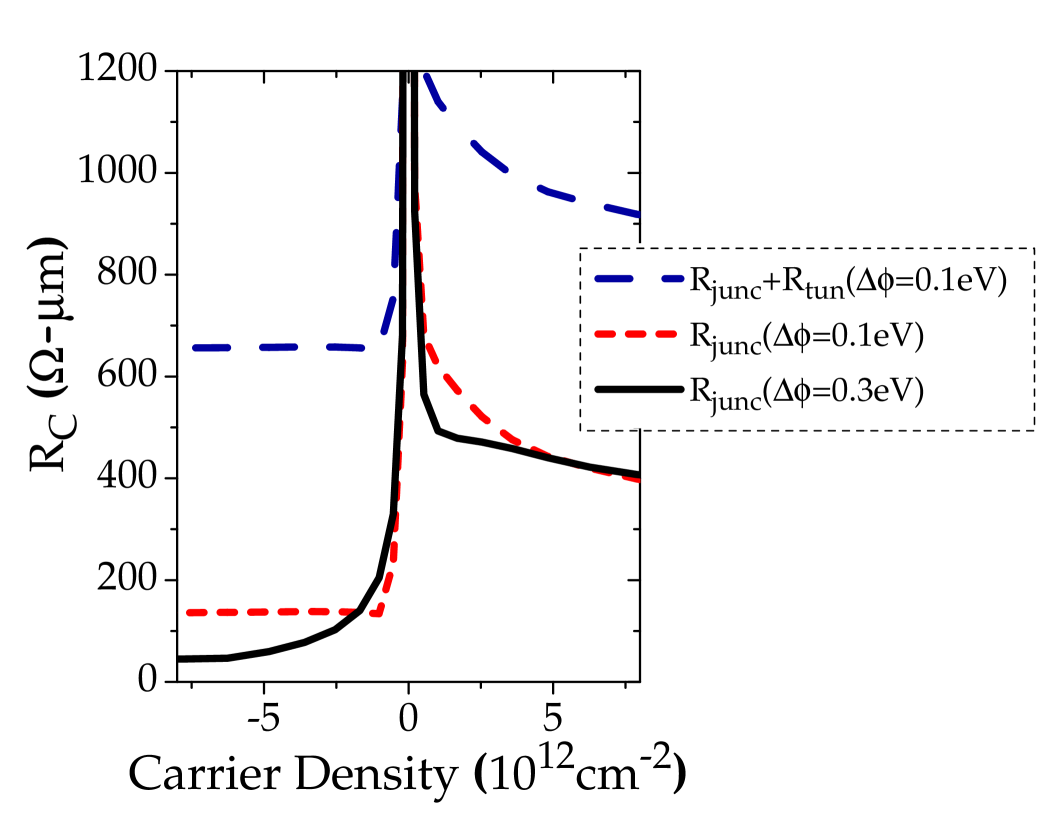
In Fig. 4, we consider the contact resistance for a pair of interfaces , incorporating both the tunneling component that we extracted previously, and the junction component assuming a work function difference (long-dashed line). It is expected that can vary considerably from experiment to experiment, due to different contact materials, interface conditions, etc. blake01 ; kim02 ; nagashio02 ; russo01 ; venugopal01 ; liu10 ; xia01 . Significant reductions in will be crucial, and the contact metal and deposition and annealing conditions will be critical factors. Recently, it was demonstrated that a low power plasma treatment prior to metal deposition is beneficial in improving robinson01 . Another very recent study demostrates that is temperature dependent, possibly due to an expansion of graphene-metal distance xia01 .
The ballistic junction component , on the other hand, seems to have a more universal nature, since it is limited by the electrostatics condition, and the number of conducting channels bottleneck Low01 . To illustrate this, we plotted for and in Fig. 4. For channel carrier concentration , a lower resistance plateau forms. The resistance value of this plateau is described by the quantum contact resistance Datta01 , where is the number of current-carrying modes, and this limit is imposed by at the metal side of the junction. Indeed for (short-dashed line), one finds -, while for (solid line) one finds -. In the latter case, however, for moderate negative values of , where the plateau hasn’t been reached, quantum resistance is limited by the number of modes in the channel, and holds valid instead. The elevated right branch, when , is due to the effect of interband tunneling. Selection of appropriate metal workfunction or approaches to engineer sharp - junction, i.e. chemical doping avouris01 , are promising directions.
In conclusion, we have proposed a model that explains the gate dependent resistance asymmetry observed in experiments, and provides increased understanding of the different components of the contact resistance in graphene transistors. We show that the existence of an interfacial layer between the metal and graphene can explain the back gating of the contacts observed by Chen and Appenzeller chen01 . The importance of such an interfacial layer to devices was also pointed out in two very recent studies. Robinson et al. show that residual photoresist following lithography can lead to high contact resistance robinson01 , and Xia et al. explain the temperature dependence of the contact resistance in terms of the graphene to metal distance xia01 . Our work and these studies point to the need for further understanding of the metal-graphene interfacial layer as a prerequisite for engineering a good contact resistance for graphene electronics.
Acknowledgement: This work has been supported by the Nanoelectronics Research Initiative through the INDEX center, and by the Focus Center for Material Structures and Devices. Computational support was provided by the Network for Computational Nanotechnology (NCN).
References
- (1) K. S. Novoselov, A. K. Geim, S. V. Morozov, D. Jiang, Y. Zhang, S. V. Dubonos, I. V. Grigorieva, and A. A. Firsov, “Electric field effect in atomically thin carbon films,” Science, vol. 306, p. 666, 2004.
- (2) K. S. Novoselov, A. K. Geim, S. V. Morozov, D. J. and.M. I. Katsnelson, I. V. Grigorieva, , S. Dubonos, and A. A. Firsov, “Two-dimensional gas of massless dirac fermions in graphene,” Nature, vol. 438, p. 197, 2005.
- (3) Y. B. Zhang, Y. W. Tan, H. L. Stormer, and P. Kim, “Experimental observation of the quantum hall effect and berry’s phase in graphene,” Nature, vol. 438, p. 201, 2005.
- (4) A. K. Geim and K. S. Novoselov, “The rise of graphene,” Nature Mat., vol. 6, p. 183, 2007.
- (5) A. H. C. Neto, F. Guinea, N. M. R. Peres, K. S. Novoselov, and A. K. Geim, “The electronic properties of graphene,” Rev. Mod. Phys., vol. 81, p. 109, 2009.
- (6) P. Avouris, “Graphene: electronic and photonic properties and devices,” Nano Letters, vol. 10, p. 4285, 2010.
- (7) F. Schwierz, “Graphene transistors,” Nature Nanotechnology, vol. 5, p. 487, 2010.
- (8) Y. M. Lin, C. Dimitrakopoulos, K. A. Jenkins, D. B. Farmer, H. Y. Chiu, A. Grill, and P. Avouris, “100 ghz transistors from wafer scale epitaxial graphene,” Science, vol. 327, p. 662, 2010.
- (9) F. Schedin, A. K. Geim, S. V. Morozov, E. W. Hill, P. Blake, M. I. Katsnelson, and K. S. Novoselov, “Detection of individual gas molecules adsorbed on graphene,” Nature Mat., vol. 6, p. 652, 2007.
- (10) K. S. Kim, Y. Zhao, H. Jang, S. Y. Lee, J. M. Kim, K. S. Kim, J.-H. Ahn, P. Kim, J.-Y. Cho, and B. H. Hong, “Large scale pattern growth of graphene films for stretchable transparent electrodes,” Nature, vol. 457, p. 706, 2009.
- (11) Semiconductor Industry Association, “The national technology Roadmap for Semiconductors” , 2010.
- (12) Z. Chen and J. Appenzeller, “Gate modulation of graphene contacts on the scaling of graphene fets,” Symp. on VLSI Tech., vol. -, p. 128, 2009.
- (13) S. Kim, J. Nah, D. S. I. Jo, L. Colombo, Z. Yao, E. Tutoc, and S. K. Banerjee, “Realization of a high mobility dual-gated graphene field-effect transistor with al2o3 dielectric,” Appl. Phys. Lett., vol. 94, p. 062107, 2009.
- (14) G. Giovannetti, P. A. Khomyakov, G. Brocks, V. M. Karpan, J. van den Brink, and P. J. Kelly, “Doping graphene with metal contacts,” Phys. Rev. Lett., vol. 101, p. 026803, 2008.
- (15) Y. Z. Y. Yu, S. Ryu, L. Brus, K. Kim, and P. Kim, “Tuning the graphene work function by electric field effect,” Nano Letters, vol. 10, p. 3430, 2009.
- (16) J. A. S. B. Huard, N. Stander and D. Goldhaber-Gordon, “Evidence of the role of contacts on the observed electron-hole asymmetry in graphene,” Phys. Rev. B, vol. 78, p. 121402, 2008.
- (17) J. Cayssol, B. Huard, and D. Goldhaber-Gordon, “Contact resistance and shot noise in graphene transistors,” Rhys. Rev. B, vol. 79, p. 075428, 2009.
- (18) M. Vanin, J. J. Mortensen, A. K. Kelkkanen, J. M. Garcia-Lastra, K. S. Thygesen, and K. W. Jacobsen, “Graphene on metals: A van der waals density functional study,” Phys. Rev. Lett., vol. 81, p. 081408, 2010.
- (19) L. M. Zhang and M. M. Fogler, “Nonlinear screening and ballistic transport in a graphene p-n junction,” Phys. Rev. Lett., vol. 100, p. 116804, 2008.
- (20) T. Low, S. Hong, J. Appenzeller, S. Datta, and M. S. Lundstrom, “Conductance asymmetry of graphene p-n junction,” IEEE Trans. Elec. Dev., vol. 56, p. 1292, 2009.
- (21) B. Huard, J. A. Sulpizio, N. Stander, K. Todd, B. Yang, and D. Goldhaber-Gordon, “Transport measurements across a tunable potential barrier in graphene,” Phys. Rev. Lett., vol. 98, p. 236803, 2007.
- (22) D. W. Boukhvalov, M. I. Katsnelson, and A. I. Lichtenstein, “Hydrogen on graphene: Electronic structure, total energy, structural distortions and magnetism from first-principles calculations,” Phys. Rev. B, vol. 77, p. 035427, 2008.
- (23) J. Chen, C. Hang, S. Xiao, M. Ishigami, and M. Fuhrer, “Intrinsic and extrinsic performance limitations of grapheme devices on SiO2,” Nature Nanotechnology, vol. 3, p. 206, 2008.
- (24) V. Perebeinos and P. Avouris, “Inelastic scattering and current saturation in graphene,” Phys. Rev. B, vol. 81, p. 195442, 2010.
- (25) S. Adam, E. H. Hwang, V. M. Galitski, and S. D. Sarma, “A self-consistent theory for graphene transport,” Proc. Nat. Acad. Sci., vol. 104, p. 18392, 2007.
- (26) A. J. Leggett, “Macroscopic quantum systems and the quantum theory of measurement,” Prog. Theor. Phys. Supp., vol. 69, p. 80, 1980.
- (27) Y. T. Hou, Y. J. M. F. Li, and W. H. Lai, “Direct tunneling hole currents through ultrathin gate oxides in metal-oxide-semiconductor devices,” Journ. of App. Phys, vol. 91, p. 258, 2002.
- (28) K. Nagashio, T. Nishimura, K. Kita, and A. Toriumi, “Contact resistivity and current flow path at metal/graphene contact,” Appl. Phys. Lett., vol. 97, p. 143514, 2010.
- (29) P. Blake, R. Yang, S. Morozov, F. Schedin, L. Ponomarenko, A. Zhukov, R. Nair, I. Grigorieva, K. Novoselov, and A. Geim, “Influence of metal contacts and charge inhomogeneity on transport properties of graphene near the neutrality point,” Solid State Comm., vol. 149, p. 1068, 2009.
- (30) S. Russo, M. Craciun, M. Yamamoto, A. Morpurgo, and S. Tarucha, “Contact resistance in graphene-based devices,” Physica E, vol. 42, p. 677, 2010.
- (31) L. C. A. Venugopal and E. M. Vogel, “Contact resistance in few and multilayer graphene devices,” Appl. Phys. Lett., vol. 96, p. 013512, 2010.
- (32) W. J. Liu, M. F. Li, S. H. Xu, Q. Zhang, Y. H. Zhu, K. L. Pey, H. L. Hu, Z. X. Shen, X. Zou, J. L. Wang, J. Wei, H. L. Zhu, and H. Y. Yu, “Understanding the contact characteristics in single or multi-layer graphene devices,” Int. Elec. Dev. Meet., 2010.
- (33) F. Xia, V. Perebeinos, Y. Lin, Y. Wu, and Ph. Avouris, “The origins and limits of metal-graphene junctrion resistance,” Nat. Nano), DOI: 10.1038, 2011.
- (34) J. A. Robinson, M. LaBella, M. Zhou, M. Hollander, R. Kasarda, Z. Hughes, K. Trumbull, R. Cavalero, and D. Snyder, “Contacting graphene,” Appl. Phys. Lett., vol. 98, p. 053103, 2011.
- (35) S. Datta, “Electronic transport in mesoscopic systems,” Camb. Univ. Press, 1995.
- (36) T. Mueller, F. Xia, M. Freitag, J. Tsang, and Ph. Avouris, “Role of contacts in graphene transistors: A scanning photocurrent study,” Phys. Rev. B), vol. 79, p. 245430, 2009.