,
Ultra-Low-Power Superconductor Logic
Abstract
We have developed a new superconducting digital technology, Reciprocal Quantum Logic, that uses AC power carried on a transmission line, which also serves as a clock. Using simple experiments we have demonstrated zero static power dissipation, thermally limited dynamic power dissipation, high clock stability, high operating margins and low BER. These features indicate that the technology is scalable to far more complex circuits at a significant level of integration. On the system level, Reciprocal Quantum Logic combines the high speed and low-power signal levels of Single-Flux-Quantum signals with the design methodology of CMOS, including low static power dissipation, low latency combinational logic, and efficient device count.
pacs:
Power consumption has increasingly become a limiting factor in high performance digital circuits and systems. According to a U.S. Environmental Protection Agency study EPA2007 , the demand of servers and data centers in the U.S. is approaching 12 GW, equivalent to the output of 25 power plants. Here we show a new logic family, Reciprocal Quantum Logic, that combines the low energy and high clock rates of superconductor devices with the essential qualities of CMOS, including low static power dissipation, low latency combinational logic, and efficient device count. On a system level, this yields a factor of 300 reduction in power compared to projected nano-scale CMOS, while taking in account the overhead of cryogenic operating temperature.
Superconducting digital electronics has long been considered the ultimate low energy alternative to CMOS ITRS04 based on the fundamental advantages of lossless interconnect and fast, low energy signal levels. Passive superconducting interconnect allows data transmission without signal amplification. Superconducting interconnects have a typical bandwidth of 700 GHz, which has allowed serial data rates up to 60 Gbs-1 for chip-to-chip communication herr02 . Lossless interconnects would enable large systems with high computational density, as compared to conventional systems where interconnect dominates the total power budget.
Unlike transistor circuits, where dissipated power is set by device size and materials, superconductor circuits are in the regime where device size and power dissipation is set by the thermal noise limit. The active device, the Josephson junction, generates quantum accurate digital information in the form of Single Flux Quanta (SFQ) of magnetic field Wb. Using equivalent units mVps2 mApH illustrates that the SFQ can exist as a transient voltage pulse across the Josephson junction or as a persistent current in a superconducting inductive loop. For a typical minimum critical current of 0.1 mA at liquid helium temperature, the SFQ pulse energy is only J. This is only about three orders of magnitude above the fundamental thermal Boltzmann limit, , and is the practical limit for classical digital circuits operating with low bit error rate. Beyond this limit there are only reversible computing and quantum computing.
Numerous circuits with record-breaking clock rates have been demonstrated in the Rapid-Single-Flux-Quantum (RSFQ) Likharev91 logic family, including a static digital divider operating up to 770 GHz Likharev99 , digital signal processors clocked at 20-40 GHz Vernik07 , aherr08 , and a serial microprocessor at 20 GHz Tanaka06 . Cryocooler-mounted prototypes have included a digital receiver used for satellite communications Mukhanov08 and high-end router components operating at 47 Gbs-1 port speed Hashimoto08 . However, the technology suffers from high overhead in static power dissipation and device count, which offset the energy advantages of SFQ data encoding. RSFQ circuits use DC power delivered on a common voltage rail via bias resistors, which is analogous to TTL logic and inferior to CMOS due to static power dissipation. Ten times more power is dissipated in the bias resistors than in the active devices even in a fully active RSFQ circuit. While the power rail voltage is only about 1 mV, it draws significant current, reaching 1 A for a circuit with 10,000 Josephson junctions. This results in high parasitic heat load in the cryopackage. Additional overhead is incurred in the timing design; RSFQ uses an active clock distribution network, which leads to significant accumulated jitter and timing variations based on device parameters and data pattern statistics. Timing design of high speed circuits results in a total device count that is dominated by the clock distribution network Kataeva06 . RSFQ is pipelined on the gate level, which enables high clock rates but also incurs high latency. The new logic family described here circumvents each of these limitations while preserving the fundamental property of SFQ data encoding.
We report a new superconducting logic family, Reciprocal Quantum Logic (RQL), that eliminates static power by replacing bias resistors with inductive coupling to an AC transmission line that effectively powers the devices in series and eliminates large ground return current. The AC power also serves as a stable clock reference signal, preventing accumulated clock jitter. The novel power supply is paired with a novel data encoding. A logical “one” is encoded as a reciprocal pair of SFQ pulses of opposite polarity. During the positive half cycle, the logic operation involves storage and routing of SFQ data pulses. While the gates have internal state with respect to the positive pulse, the trailing negative-polarity SFQ pulse serves as a reset. This greatly simplifies gate design and produces combinational logic behavior. Similar to CMOS, these combinational gates allow multiple levels of logic per stage for low latency. Overall, RQL combines the high speed and low-power signal levels of SFQ signals with the design methodology of CMOS.
Using simple experiments involving logic gates and a 1600-device shift register and logic gates, we have demonstrated that RQL is at once high speed and low energy with a low bit-error rate. We measure energy dissipation to be within a factor of 1000 of the thermal limit at clock rates in the range 2-10 GHz for the shift register, and negligible BER of less than for the logic gates while maintaining operating margins of 30%. AC power is supplied to the circuit on superconductor microstrip transmission line, which also serves as a passive clock distribution network. We show high stability of the clock at frequencies up to 12 GHz. The technology scales to the one-million device level clocked at 6 GHz with only a 6 mW power supply, amounting to only 15 mA on a 50 line with dynamic timing variation of only 1% of the clock period. This indicates that the technology is scalable to complex circuits at a significant level of integration. Computational efficiency of the circuits is nearly three orders of magnitude higher in terms of operations per Joule compared to high performance CMOS. Taking into account that superconductor circuits require a cryocooler, with efficiency of 1,000 W/W achievable at 4.2 Kelvin, RQL circuits offer a system-level factor of 300 less wall-plug power dissipation. This makes RQL technology attractive for many applications, including high end computing.
Results
Power dissipation. RQL circuits have zero static power dissipation, so for the first time dynamic power dissipation in a superconducting SFQ circuit could be measured directly. The clock power is carried on 50 lines that return to room temperature without termination on chip, allowing direct measurement of the relative amplitude of the output waveforms for an inactive and fully active circuit. Because dynamic power dissipation is so small, the experiment requires a circuit with a large number of Josephson junctions and a low AC power amplitude with relatively high coupling to the clock line. The shift register was chosen as a convenient test vehicle.
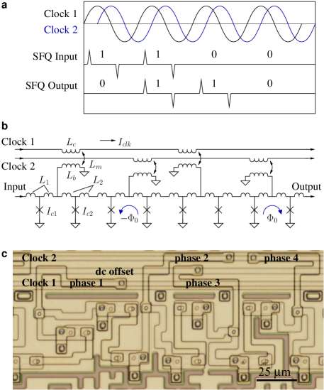
Fig. 1 shows the schematic and physical layout of one bit of the RQL shift register circuit. The four-phase clock is a fundamental feature that provides directionality. Without this, the positive pulse that moves forward during the positive half clock cycle would travel backward during the negative half of the cycle, annihilating the negative pulse. Instead, the positive pulse rides the leading edge of the clock from one phase to the next and arrives at the output after one cycle of delay, and the negative pulse follows with half a cycle of separation.
A 200-bit shift register with 1600 Josephson junctions was fabricated in a commercial superconductor fabrication process with 4.5 kA cm-2 Josephson junction critical current density, 1.5 m minimum feature size, and four metal layers Hypres . The junction plasma frequency is 250 GHz, corresponding to an SFQ pulse width of 3 ps at critical damping. The impedance of the power transmission line, implemented as microstrip with 2.3 m minimum line width and SiO2 dielectric thickness of 850 nm, is limited to 32 including parasitic capacitive coupling to the bias inductors of about 7 fF. Impedance matching to 50 was accomplished with tapered microstrip lines leading to the contact pads.

The data in Fig. 2 correspond to the power dissipated in a fully active circuit with an all “ones” input pattern relative to the inactive case of all “zeros”. Using the estimate , energy dissipation per digital “one” is J with average A. Total power dissipation of the circuit would scale with the number of Josephson junctions and clock frequency. Measured power dissipation in the circuit is three times smaller than this estimate. Additional data points corresponding to a 6 Gbs-1 pseudo-random input pattern show W total power dissipation in the 800 Josephson junctions on each clock line. This is half the power dissipation of the all “ones,” as expected, and is only three orders of magnitude above the von Neumann-Landauer thermal limitLandauer , per bit.
A model for SFQ dissipation based on the energy potential indicates that the work done on a switching junction is a function of bias current rather than critical current BaronePaterno . Physical-level simulation whiteley of the circuit shows that in the range of interest, where clock period is much longer than the switching time of the Josephson junctions, data pulses pass through each stage early in the clock cycle under low bias conditions. This results in a low energy SFQ pulse with simulated dissipation of about at 6 Gbs-1. Switching of the Josephson junctions is shifted to higher bias at higher frequency, producing a slightly non-linear frequency dependence. Experimental data agreess with this simulation result fit with a single prefactor of 1.35.
Clock phase stability. Switching of Josephson junctions not only attenuates the AC clock but also adds accumulative delay. The magnitude of this effect can be estimated using a simple linear model where the Josephson junction acts as an inductor if superconducting, and as a resistor if switching. The clock propagation time in the case of all digital “ones” is the same as for an isolated line =7.6 fs/m, where = 0.3 pH/m, = 0.29 fF/m are the clock line inductance and capacitance in the circuit. In the case of all digital “zeros”, propagation time is with inductance given by the impedance transformation for inductive coupling
| (1) |
where is the bias inductor and is the magnetic coupling constant as shown in Fig. 1b. is the inductance of the RQL gate connected to the bias inductor. In the shift register, is the series and parallel combination of the interconnect and the Josephson inductances . In general terms, data-dependent phase delay of the clock scales as and can be minimized by reducing coupling to the clock line and increasing AC clock power.
Accumulated variable clock delay for the entire 200-bit shift register is 1.40.2 ps and is independent of frequency. Variable delay was directly observed on the clock return from the chip at 2-12 GHz on a sampling oscilloscope to compare the data patterns of all “ones” and all “zeros”. Accuracy was limited by drift between the two phase-locked synthesizers that clocked the chip and triggered the oscilloscope. This result is in agreement with the analytical estimate of Eq. 1, which gives 1.5 ps variable clock delay for the complete 200-bit shift register circuit.
Logic gates. Routing and processing of pulse-based signals is distinct from transistor-based voltage-state logic, as shown in Fig. 3. Logical A-and-not-B (AnotB) means that an input pulse A will propagate to output Q unless a pulse on input B comes first. Logical And & Or (AndOr) means that the first input pulse, if any, goes to Q1 (logical OR), and the second input pulse goes to Q2 (logical AND). Inputs to the AnotB gate must satisfy the timing requirement that B arrive before A generates an output. There is no similar timing requirement for the AndOr gate.
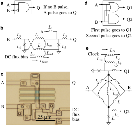
The logical behavior of the gates is based on the reciprocal data encoding. Considering only the positive pulses, the gates are similar to the state machines of RSFQ logic, as input changes the internal flux state of the inductive loops. However, the trailing negative pulse erases the internal state every clock cycle and produces combinational logic behavior. The reset operation afforded by the negative pulse greatly simplifies the logic design, so that each gate consists of only two active devices with inductive interconnect. The gates have large parametric operating margins, including simulated tolerances on junction critical currents of at least 50%.

On the physical level, both RQL gates have a bistable internal flux state corresponding to . The AnotB gate has an explicit flux bias line that sets up positive current through both junctions to ground. When either junction is triggered by an SFQ pulse, the flux state is reversed, which reverses current through the junctions and inhibits triggering of the opposite junction. The AndOr gate has an implicit flux bias on inductor , as the bias inductor is connected at the end that favors the OR output. Triggering of OR output redirects the bias current through to the AND output. The gates require high efficiency transformers that provide high common-mode inductance, when currents through the inductors are in the same direction, and low differential mode inductance. In the AnotB gate, the transformer inverts the polarity of the signal between input B and the output. In the AndOr gate, the transformers aid propagation of either input pulse to the outputs, but inhibit propagation of input to the opposite input.
RQL logic gates cannot drive each other directly, but need at least one interconnect cell to achieve fanout of one. The interconnect cell is similar to the two-junction shift register unit cell, but with some reduction of bias current to junctions interior to the clock phase boundaries. The standard requirement of fanout equal to four can be achieved using seven interconnect cells arranged in a binary tree. The four phase clock provides an implicit pipeline without additional devices for latches or clock distribution. Large circuit blocks with multiple levels of logic can be on a single clock phase for low latency, or smaller blocks can be used in a deeper pipeline for higher maximum clock rate. A crucial property of the RQL pipeline is self-correcting timing. A pulse arriving early at a phase boundary will be delayed due to low bias current. A late pulse will arrive during high bias and will be accelerated. Pulses travelling through the pipeline constantly tend toward timing equilibrium. However, at too high a clock rate a late pulse will arrive at the phase boundary on the falling edge of the clock and will be delayed further, causing failure. The maximum clock frequency is determined by the number of switching events per phase during approximately one quarter of the clock period.
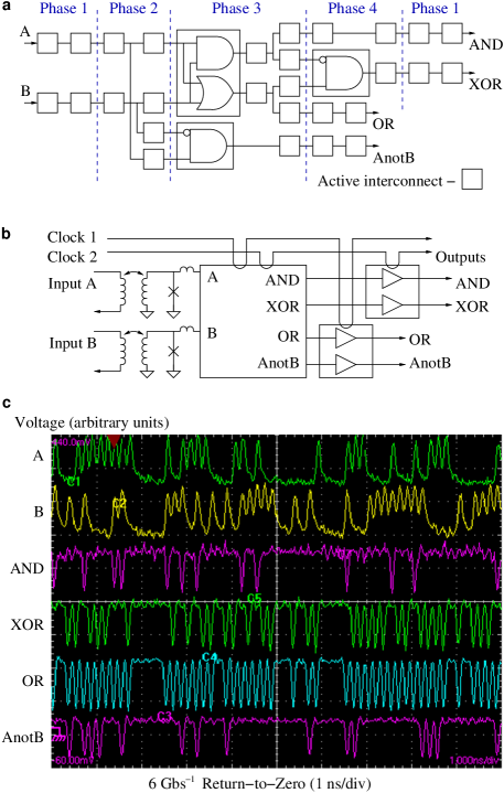
Fig. 4 shows the RQL logic test circuit. The circuit consists of an AndOr gate, two AnotB gates, and interconnect. The circuit has two inputs and four outputs to produce the logic functions OR, XOR, AND, and AnotB. Logical XOR is synthesized using an AndOr gate followed by an AnotB. Total latency through the circuit is one clock cycle. The timing requirement of each AnotB gate is satisfied by placement on a clock phase boundary, with gate output controlled by the trailing clock phase of the output interconnect. With this arrangement the relative timing of inputs A and B is not important, as both input are certain to arrive before the output is generated.
The logic circuit was collocated on the same chip as the shift register. The complete circuit includes input gates that convert a return-to-zero (RZ) waveform to RQL data encoding, and output amplifiers that convert back to RZ voltage levels. The distributed output amplifier, similar to that described in Herr10 , provides a 2 mV signal. At the 1.5 m lithography node the logic circuit itself was designed for 20 GHz operation, but was limited in test to 6 GHz by the input pattern generator. Measured operating margins on clock power were 25%, limited on the low end by the output amplifers, and on the high end by overbiasing of the logic circuit. Similar operating margins were measured at the lower frequency of 2 GHz.
Bit-Error Rate SFQ circuits operate in the thermal limit, with device size ultimately determining both energy dissipation and bit-error rate (BER), which must be considered in conjunction with each other. Fig. 5 shows the BER of the AnotB gate clocked at 6 GHz, measured by monitoring the logical XOR output while setting the flux bias on the gate to values near failure. At the nominal point, the flux bias provides symmetry between the bi-stable flux states in the gate. At low bias, the observed failure is of logical “ones” becoming logical “zeros” uniformly throughout the pattern; at high bias, logical “zeros” become logical “ones”. Both error modes indicate switching errors of the junction, labeled , that generates the output.
The data are fit to a Gaussian distribution with bit-error rate
| (2) |
where is the distance of the flux bias current from the error threshold , and is the root-mean-square noise current. The prefactor takes into account that for either error mode only half of the bits in the pattern contribute to the error rate. The factor of twenty represents the transfer function between applied flux bias and current induced in the loop containing the Josephson junctions. Numerical fits were obtained with less than 1% asymptotic standard error. On the left, mA and A; on the right, mA and A. At the optimal bias point of 1.82 mA, the data extrapolate to negligible BER for the gate under test. The lowest rate actually measured is below for the entire circuit, including the output data link.
Discussion
The extrapolated minimum BER in our test indicates that device size and power could be scaled down still further. The error mechanism may involve either storage errors KleinMukherjee , decision errors Filippov91 , or even timing errors in an over-clocked circuit LikharevRylyakov99 . In all of these cases, noise current scales as the square root of the Josephson critical current, while the current scale of the error threshold goes linearly. Applying this scaling to Eq. 2 indicates that device size could be reduced by a factor of ten and still extrapolate to a minimum error rate of 10-44, which is negligible even for the most demanding applications including high-end computing. As a practical matter, BER below 10-44 could be maintained over a wide flux bias margin of % by scaling device size down by a factor of four. Measured noise current in our test is consistent with previous results for the gray zone of the RSFQ comparator Filippov97 , Filippov95 , but with much lower bit error rates relative to RSFQ circuits HerrAPL96 ; Bunyk99 ; Herr99 due to the larger operating margins in RQL.
The chip power scales linearly with number of junctions and frequency. We measured that with a 12.6 W power supply, 800 junctions clocked at 6 GHz have a worst-case data-dependent power ratio of 0.91, corresponding to a variation in bias current amplitude of %. Such a circuit scaled to junctions and with a manageable maximum bias current variation of % would require a 6 mW power supply, amounting to only 15 mA of current on a 50 line. On the same circuit we measured a 1.4 ps worst-case variable clock propagation delay, independent of frequency. The given junction circuit would correspond to twenty times less coupling to the clock line. Because variable clock delay scales as this circuit would have a timing variation of only 5 ps, or only % of the clock period at 6 GHz. The AC clock provides a stable clock reference that suppresses accumulative clock jitter, so ultimately clock frequency is limited by the switching time of the Josephson junction, which scales linearly with feature size. At the 0.8 m lithography node, we can expect a 70 GHz maximum clock frequency Abelson04 , or alternately a 6 GHz operation with twelve levels of logic per pipeline stage.
AC power distribution on-chip will benefit from the exceptional microwave properties of superconducting materials that have found applications ranging from single-photon qubit resonators with Q of to THz dark matter detectors Vion08 ; Detectors . Monolithic integration of RQL gates with microwave components, including power splitters, matching networks, and phase shifters, is a strength of the technology. Power dissipation in these passive components is as low as 1% per wavelength Nblosses ; Nblosses1THz , which would correspond to only 2.3% of the applied power in our shift register experiment. In the cryopackage, a 15 mA amplitude for the clock is consistent with low heat transport on the wires Cryo-Gupta . Very high clock rates up to 71 GHz have already been demonstrated for Josephson voltage standards using waveguides in the cryopackage PTB ; NIST .
Computational efficiency of the measured circuits are approaching with further reductions expected using smaller devices, giving unmatched efficiency in terms of operations per Joule. This means the technology offers a low energy solution for high end computing even after taking into account the overhead of the cryocooler, on the order of 1000 W/W at 4.2 K Coolers . Because the 700 GHz energy gap in Nb makes superconductors inherently radiation-hard King91 , the technology may be useful for computationally intensive applications in space. Since device size and power can be scaled with temperature to remain in the noise-limited regime, the technology would be ideal for classical control, readout, and error-correction feedback for solid state qubits QubitControl operating at millikelvin.
Acknowledgements.
This work was supported in part by the Defense Micro-Electronics Activity under the Advanced Technology Support Program. The authors thank Marc Manheimer for discussion, John Fusco for administration, and acknowledge assistance from Isaac Carruthers with the software design environment, from Donald Miller and Steve Shauck with the design.References
- (1) Data Center Report to Congress, U.S. Environmental Protection Agency, www.energystar.gov, (2007).
- (2) ITRS 2004 Update: Emerging Research Devices, Intern. Technol. Roadmap for Semicond., www.itrs.net/links/2004Update/2004_05_ERD.pdf (2004).
- (3) Q.P. Herr, A.D. Smith and M.S. Wire, High speed data link between digital superconductor chips, Appl. Phys. Lett., 80 (2002), pp. 3210–3212.
- (4) K.K. Likharev and V.K. Semenov, RSFQ logic/memory family: a new Josephson-Junction digital technology for sub-terahertz-clock-frequency digital systems, IEEE Trans. Appl. Supercond., 1 (1991), pp. 3–28.
- (5) W. Chen, A.V. Rylyakov, V. Patel, J.E. Lukens and K.K. Likharev, Rapid Single Flux Quantum T-Flip Flop operating up to 770 GHz, IEEE Trans. Appl. Supercond., 9 (1999), pp. 3212–3215.
- (6) I.V. Vernik, D.E. Kirichenko, et. al., Cryocooled Wideband Digital Channelizing RF Receiver Based on Low-Pass ADC, Ext. Abs of ISEC’07, Washington (2007), pp. 71–74.
- (7) A.Y. Herr, RSFQ baseband digital signal processing, IEICE Trans. Electron., E91-C, (2008), pp. 293–305.
- (8) M. Tanaka, T. Kawamoto, Y. Yamanashi, Y. Kamiya, A. Akimoto and K. Fujiwara, Design of a pipelined 8-bit-serial single-flux-quantum microprocessor with multiple ALUs, Supercond. Sci. Technol., 19, (2006), S344.
- (9) O.A. Mukhanov, D. Kirichenko, et. al., Superconductor Digital-RF Reciever Systems, IEICE Trans. Electron., E91-C. (2008), pp. 306–317.
- (10) Y. Hashimoto, S. Yorozu and Y. Kameda, Development of Cryopackaging and I/O technologies for high-speed superconductive digital systems, IEICE Trans. Electron., E91-C, (2008), pp. 325–328.
- (11) I. Kataeva, H. Engseth and A. Kidiyarova-Shevchenko, New Design of an RSFQ Parallel Multiply-Accumulate Unit, Supercond. Sci. Technol., 19, (2006), S381.
- (12) Hypres Nb design rules, www.hypres.com, (2010).
- (13) R. Landauer, Irreversibility and heat generation in the computing process, IBM J. Res. and Devel., 5, (1961), pp. 183–191.
- (14) A. Barone and G. Paterno, Physics and Applications of the Josephson Effect, Wiley, (1982), Chap 6.
- (15) S.R. Whiteley, Josephson junctions in SPICE3, IEEE Trans. Magn., 27, (1991), pp. 2902–2905.
- (16) Q.P. Herr, A high-efficiency superconductor distributed amplifier, Supercond. Sci. Technol., 23, (2010), 022004 (4pp).
- (17) M. Klein and A. Mukherjee, Thermal noise induced switching of Josephson logic devices, Appl. Phys. Lett., 40, (1982), pp. 744–747.
- (18) T.V. Filippov and V.K. Kornev, Sensitivity of the balanced Josephson-junction comparator, IEEE Trans. Magn., 27, (1991), pp. 2452–2455.
- (19) A.V. Rylyakov and K.K. Likharev, Pulse jitter and timing errors in RSFQ circuits, IEEE Trans. Appl. Supercond., 9, (1999), pp. 3539–3544.
- (20) V.K. Semenov, T.V. Filippov, Y.A. Polyakov and K.K. Likharev, SFQ balanced comparators at a finite sampling rate, IEEE Trans. Appl. Supercond., 7, (1997), pp. 3617–3621.
- (21) T.V. Filippov, Y.A. Polyakov, V.K. Semenov and K.K. Likharev, Signal resolution of RSFQ comparators, IEEE Trans. Appl. Supercond., 5, (1995), pp. 2240–2243.
- (22) Q.P. Herr and M.J. Feldman, Error rate of a superconducting circuit, Appl. Phys. Lett., 69, (1996), pp. 694–695.
- (23) P. Bunyk and P. Litskevitch, Case study in RSFQ design: fast pipelined parallel adder, IEEE Trans. Appl. Supercond., 9, (1999), pp. 3714–3720.
- (24) Q.P. Herr, M.W. Johnson and M.J. Feldman, Temperature-dependent bit-error rate of a clocked superconducting digital circuit, IEEE Trans. Appl. Supercond., 9, (1999), pp. 3594–3597.
- (25) L.A. Abelson and G.L. Kerber, Superconductor integrated circuit fabrication technology, Proceedings of the IEEE, 92, (2004), pp. 1517–1533.
- (26) A. Palacios-Laloy, F. Nguyen, F. Mallet, P. Bertet, D. Vion and D. Esteve, Tunable resonators for quantum circuits, J. Low Temp. Phys., 151, (2008) pp. 1034–1042.
- (27) J. Zmuidzinas and P.L. Richards, Superconducting detectors and mixers for millimeter and submillimiter astrophysics, Proceedings of the IEEE, 92, (2004), pp. 1597–1616.
- (28) A. Vayonakis, C. Luo, H.G. Leduc, R. Schoelkopf and J. Zmuidzinas, The millimeter-wave properties of superconducting microtrip lines, AIP Conf. Proc., 605, (2002), pp. 539–542.
- (29) M. Bin, M.G. Gaidis, J. Zmuidzinas and T.G. Phillips, Low-noise 1 THz niobium superconducting tunnel junction mixer with a normal metal tuning circuit, Appl. Phys. Lett., 68, (1996), pp. 1714–1716.
- (30) D. Gupta, A.M. Kadin, et. al, Integration of cryocooled superconducting Analog-to-Digital converter and SiGe output amplifier, IEEE Trans. on Appl. Supercond., 13, (2003), pp. 477–483.
- (31) L. Palafox, G. Ramm, R. Behr, W.G.K Ihlenfeld and H. Moser, Primary AC power standard based on programmable Josephson junction arrays, IEEE Trans. Instrum. Meas., 56, (2007), pp. 534–537.
- (32) S.P. Benz and C.A. Hamilton, Application of the Josephoson effect to voltage metrology, Proceedings of the IEEE, 92, (2004), pp. 1617–1629.
- (33) R. Radebaugh, Cryocoolers: the state of the art and recent developments, J. Condens. Matter, 21, (2009), 164219 (9pp).
- (34) S.E. King, R. Magno and W.G Maisch, Radiation damage assessment of Nb tunnel junction devices, IEEE Trans. Nuc. Sci., 38, (1991), pp. 1359–1364.
- (35) V.K. Semenov and D.V. Averin, SFQ control circuits for Josephson junction qubits, IEEE Trans. Appl. Supercond., 13, (2003), pp. 960–965.