Spin filling of valley-orbit states in a silicon quantum dot
Abstract
We report the demonstration of a low-disorder silicon metal-oxide-semiconductor (Si MOS) quantum dot containing a tunable number of electrons from zero to . The observed evolution of addition energies with parallel magnetic field reveals the spin filling of electrons into valley-orbit states. We find a splitting of 0.10 meV between the ground and first excited states, consistent with theory and placing a lower bound on the valley splitting. Our results provide optimism for the realization in the near future of spin qubits based on silicon quantum dots.
pacs:
71.55.-i, 73.20.-r, 76.30.-v, 84.40.Az, 85.40.Ry1. Introduction
Semiconductor quantum dots Kouwenhoven1997 are islands to which electrons can be added one by one by means of an electric field. Like real atoms they have discrete quantum levels and can exhibit phenomena such as shell filling Tarucha1996 , where orbital levels are filled by spin-paired electrons to produce a spin-zero many-electron state. Quantum dots also provide a promising platform for spin qubits, which can have long coherence times due to the weak coupling of spins to local fluctuations in charge. For a quantum dot to be useful as a spin qubit it is essential to understand the details of its excitation spectrum and its spin-filling structure. One powerful method to probe the spin filling is via magnetospectroscopy. This has been applied to both vertical Tarucha1996 and lateral GaAs/AlGaAs quantum dots Ciorga2000 , showing ground-state spin filling in agreement with Hund’s rule.
Silicon devices are attractive for spin-based quantum computing Loss1998 ; Kane1998 and spintronics Zutic2004 because of their scalability and long spin coherence times Tyryshkin2003 . Silicon quantum dots, in particular, have potential as electron-spin qubits, but to date it has not been possible to create devices with the low disorder present in their GaAs counterparts Tarucha1996 ; Ciorga2000 . This is primarily due to disorder at the Si/SiO2 interface, which has made it difficult to achieve single-electron occupancy Lim2009 ; Xiao2010 .
In addition, the conduction band structure in silicon is complex and only a few experiments have been carried out to examine the spin states in either Si MOS or Si/SiGe quantum dots Xiao2010 ; Rokhinson2001 ; Hu2009 ; borselli2010 ; Simmons2010 . The valley degree of freedom makes the measurement and interpretation of spin states in all silicon-based dots non-trivial Hada2003 ; Culcer2010 , while for Si MOS dots the substantial amount of disorder usually present at the Si/SiO2 interface impedes the ability to make smooth potential wells.
In this work we present the investigation of a Si MOS quantum dot with lower disorder than any studied to date, in which it is possible to analyse the electron occupancy in a manner previously inaccessible. We deduce the spin filling of the first 12 electrons in the dot from ground-state magnetospectroscopy measurements. The formation of a two-electron () spin-singlet state at low magnetic fields confirms that there is no valley degeneracy present, while the magnetic field dependence of the higher-order Coulomb peaks allows us to deduce the level structure for the first four electrons.
In the following section we present the architecture of the quantum dot and the charge stability diagram in the few-electron regime. We then, on section 3, study the valley-orbit states in this quantum dot and extract a valley-orbit splitting of 0.10 meV. In section 4 we investigate the spin filling of the first 4 electrons in this quantum dot in detail. We then present the spin filling of the 5 to 12 electrons, discussing some anomalies observed, before concluding in section 6.

2. Low-disorder silicon MOS quantum dot
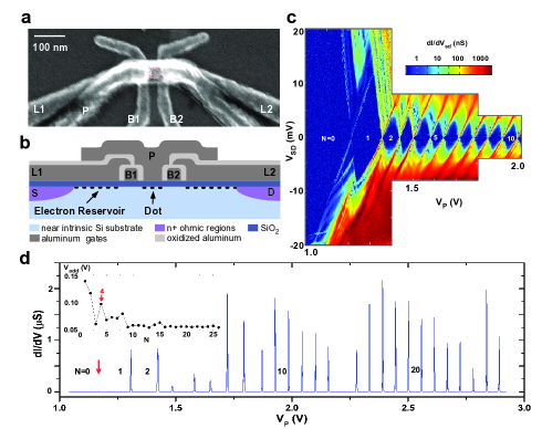
The triple-layer gate stack in our structure (Figure 1a and 1b) provides excellent flexibility for tuning the barrier transparency and the energy levels of the dot independently, see Supplementary Information for fabrication processes. The lowest layer defines the barrier gates (B1 and B2). They are used to define the dot spatially and control the tunnel coupling. The second layer of gates defines the soure-drain leads (L1 and L2). The lead gates induce the electron accumulation layers that act as source-drain reservoirs. The plunger gate (P) extends over the barrier gates, lead gates and the dot island, and is used to control the electron occupancy of the dot. Figure 1c is a plot of the differential conductance of the device versus plunger gate voltage and source-drain voltage , showing the familiar “Coulomb diamond” charge stability map. Before the first charge transition the diamond edges open entirely to a source-drain voltage 20 mV, because the quantum dot has been fully depleted of electrons. We have previously reported a device with similar gate architecture but an accidental parallel quantum dot created distortion of the charge stability map in the few-electron regime, complicating the interpretation of the dot’s level structure Lim2009 . Here, clear and sharp Coulomb peaks mark the first 27 electrons entering the dot, see Fig. 1d, while the charge stability map of Fig. 1c shows no distortions from disorder potentials.
As with quantum dots in GaAs/AlGaAs Tarucha1996 , shell
filling has very recently been observed in Si/SiGe quantum dots,
with a filled shell structure observed for
electrons borselli2010 . The addition spectrum of our Si MOS
quantum dot (inset of Figure 1d) also shows a noticeable peak at
. A filled shell at would be consistent with the filling
of a first orbital state in a two-valley system, however, an
accurate description of orbital and valley levels in silicon quantum
dots is somewhat more complex, as described below.
3. Valley-orbit splitting
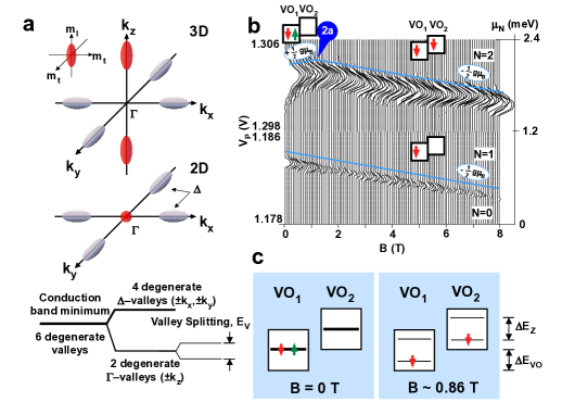
In recent years, valley physics in silicon has been studied extensively both theoretically Boykin1994 ; Friesen22010 ; Saraiva22010 ; Culcer2010 ; Saraiva2009 ; Friesen2010 ; Saraiva2010 ; Culcer22010 and experimentally kohler1979 ; Takashina2006 ; Goswami2007 ; Fuechsle2010 . In bulk silicon, there are six degenerate conduction band minima (valleys) in the Brillouin zone, as depicted in Figure 2a. Confinement of electrons in the -direction at the Si/SiO2 interface lifts the six-fold valley degeneracy: four -valleys with a heavy effective mass parallel to the interface have an energy several tens of meV higher than the two -valleys Ando1982 . The sharp and flat interface produces a potential step in the -direction and lifts the degeneracy of the -valleys in two levels separated by the valley splitting . Theoretical predictions for the valley splitting are generally on the order of 0.1–0.3 meV Culcer2010 ; Saraiva2010 . Experimental values in Si inversion layers mostly vary from 0.3–1.2 meV kohler1979 . A very large valley splitting of 23 meV in a similar structure has also been measured Takashina2006 and is explained in Saraiva22010 ; Saraiva2010 . Recently, resonant tunneling features spaced by 0.1 meV in a single-crystal silicon quantum dot were attributed to valley excited states Fuechsle2010 , while measurements on Si/SiGe quantum dots revealed valley splittings in the range of 0.12–0.27 meV borselli2010 .
Valleys and orbits can also hybridise Friesen2010 , making it inappropriate to define distinct orbital and valley quantum numbers. Depending on the degree of mixing, the valley-orbit levels behave mostly like valleys or like orbits. Instead of referring to a pure valley splitting we therefore adopt the term valley-orbit splitting, for the difference in energy between the first two single-particle levels, and . This is sometimes referred to as the ground-state gap Friesen2010 .
Full electrostatic control of the electron number allows us to investigate the spin filling by measuring the magnetic field dependence of the electrochemical potential , which is by definition the energy required for adding the electron to the dot. The slope of is given by Hada2003
| (1) |
where is the g-factor, the Bohr magneton eV/T and is the change in total spin of the dot when the electron is added. The electrochemical potential has a slope of when a spin-up electron is added, whereas addition of a spin-down electron results in a slope of . The rate at which changes with magnetic field thus reveals the sign of the added spin. For the experiments in this work we apply the magnetic field to the Si/SiO2 interface.

The conductance at the first two charge transitions is plotted as a function of the electrochemical potential energy and the magnetic field in Figure 2b. Here, the Coulomb peak positions in gate voltage are converted to electrochemical potential using the lever arm extracted from the corresponding Coulomb diamonds. The blue lines above the Coulomb peaks are guides for the eye with slopes of , as predicted by equation (1) using = 2 for bulk silicon. Since the first Coulomb peak moves down in energy with increasing magnetic field the peak corresponds to a spin-down electron entering the quantum dot, as expected for the ground state. For T the second Coulomb peak also falls in energy with increasing at a rate close to , however, for low magnetic fields the peak noticeably increases in energy with , leading to a “kink” (marked 2a) at T. This kink (2a) is confirmed by several repeated measurements over positive and negative magnetic field, see Supplementary Information (Fig. S2). These results imply that at low magnetic field (before the kink), the second electron fills the quantum dot with its spin up. As we increase the magnetic field (after the kink), the sign of the second electron spin changes from up to down at T. We note that in previous measurements on a similar quantum dot device, disorder and instability made it difficult to accurately probe this kink feature Lim2009 .
We explain the sign change observed here with a simple model where the two lowest valley-orbit levels are separated by the valley-orbit splitting , see Figure 2c. At zero magnetic field, the first two electrons fill with opposite spins in valley-orbit level 1. When a magnetic field is applied, the spin-down and spin-up states are split by the Zeeman energy . Above 0.86 T the spin-up state of valley-orbit level 1 (VO1) is higher in energy than the spin-down state of valley-orbit level 2 (VO2) and it becomes energetically favoured for the second electron to occupy the latter, i.e. VO2. At the kink the valley-orbit splitting equals the Zeeman energy, which is 0.10 meV at 0.86 T. With the interfacial electric field of 2 V/m extracted from Technology Computer-Aided-Design modeling for our device structure, the valley-orbit splitting agrees well with modeling results (0.08–0.11 meV) based on the effective-mass approximation Saraiva2010 ; Culcer22010 . We note that if no valley-orbit mixing were present, then meV would place a lower bound on the valley splitting for this structure.
For T the first two electrons fill two different levels split by = 0.10 meV. We note that the presence of a doubly degenerate ground-state level would demand the two electrons to exhibit parallel spin filling starting from 0 T, since the two electrons would then occupy two different valley states in order to minimise the exchange energy Hada2003 . A valley-degenerate state is therefore ruled out by the results in Figure 2b.
To assess the degree of valley-orbit mixing we compare the expected
values for the orbital level spacing and the valley splitting. As
stated above, theoretical calculations of the latter predict
0.1–0.3 meV. An estimate of the orbital level spacing in a quantum
dot is given by Kouwenhoven1997 ,
where () is the valley (spin) degeneracy, the
electron effective mass and the dot area. For non-degenerate
valleys, and . Using the effective mass of ,
and the lithographic dot area of nm2 we obtain
an expected orbital level spacing of 0.7 meV. This value is
considerably larger than the lower bound on the valley splitting,
suggesting that the first two levels may be valley-like, however, to
maintain generality we will continue to refer to the levels as
valley-orbit states.
4. Spin filling of the first 4 electrons
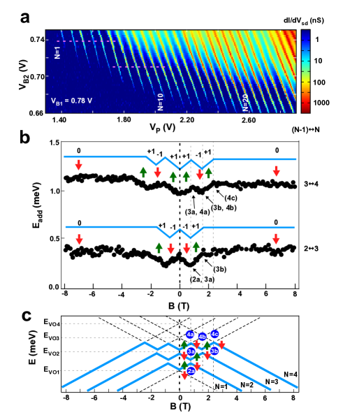
We now turn to the spin filling for electrons. Figure 3a shows the differential conductance as a function of plunger gate voltage and barrier gate voltage . The highly regular pattern of parallel Coulomb peak lines again demonstrates the low disorder in this device. In order to determine the spin filling for higher electron numbers we investigate the difference between successive electrochemical potentials as a function of magnetic field. The resulting addition energies have slopes which depend on the spin filling of two consecutive electrons, according to hanson2007
| (2) | ||||
where the first (second) arrow depicts the spin of the () electron respectively.

Figure 3b plots the measured addition energies, , for to electrons for magnetic fields in the range of T T. We see that the data in Fig. 3b tend to follow , as expected from Equation (2). Furthermore, the data is relatively symmetric about , indicating that the trends are real and not measurement artefacts. As a guide to the eye, we also show lines with slopes of exactly 0, (blue lines in Fig. 3b) that we interpret the to be following. While in regions the match is not exact, we propose that these trend lines are the best qualitative fit to the data. We are thus able to infer spin states for each of the first 4 electrons at all values of magnetic field T. These spin states are labelled with red (green) arrows, representing spin down (up), in Fig. 3b.
We now focus on the spin states of the these four electrons, to . At low magnetic fields ( T), the electrons populate the quantum dot ground states with alternating spin directions: . Conversely, at high magnetic fields ( T) a configuration with four spin-down electrons has least energy: . Recently, parallel spin filling in a Si quantum dot was explained as a result of a large exchange energy and an unusually large valley splitting of 0.77 meV Xiao2010 . When the level spacing is smaller than the exchange energy, it is energetically favoured for two electrons to occupy two consecutive levels with the same spin sign. This is not the case for the device measured here: the anti-parallel spin filling of the first two electrons below 0.86 T is only possible in case of a small exchange energy (less than ). This is an unexpected result for a dot of this size where the exchange energy is predicted to be larger than the orbital level spacing Hada2003 . Possibly the Coulomb interaction in the dot is strongly screened by the plunger gate. This is not unlikely since the distance from gate to dot (10 nm) is smaller than the dimensions of the dot itself (3060 nm).
In Figure 3c, we illustrate the magnetic-field evolution of four
non-degenerate valley-orbit levels by means of an elementary model.
Each level splits into spin-up and spin-down levels in finite
magnetic field. We assume that the exchange interaction is small in
comparison to the level spacing. The level crossings that follow
from our model fit the kinks observed in the first four Coulomb
peaks. The observed kink positions yield three valley-orbit levels
which are 0.10, 0.23 and 0.29 meV above the lowest ground state
level. The extracted level spacings for the first four valley-orbit
states are then: meV;
meV; and
meV.

5. Spin filling of electrons 5–12
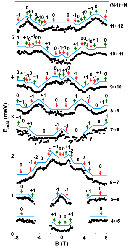
Finally in Figure 4, we plot the addition energies as a function of for electrons to 12. Once again, we predominantly observe slopes of , as expected from Equation (2). Occasionally, e.g. at , a segment has a slope of , because the total spin on the dot changes by more than . This can occur due to many-body interactions on the dot and lead to spin blockade Weinmann1995 . The latter phenomenon could also explain the suppression of current in the fifth charge transition at 5 T Rokhinson2001 ; Hu2009 ; Hada2003 .
Also, the picture of alternating spin filling below 0.8 T no longer holds
for . Unexpectedly, the fifth electron is spin up at low
magnetic field, while the lowest-energy configuration predicts a
spin-down state. This anomaly could be explained by an extra
electron in a dot nearby, which alters the spin configuration of the
main dot. Such a small dot can be created at high plunger gate
voltages, where the potential well differs from a perfect parabola. As more electrons are added to the main dot, the wavefunctions extend further and would have more opportunity to spin-couple to the unintentional dot nearby, thus affecting the spin filling of electrons.
6. Conclusion
The results here show that silicon MOS quantum dots can be fabricated with the low levels of disorder necessary to form well-defined electron spin qubits in a host material that can be made almost free of nuclear spins. The excellent charge stability allows the spin states of the dot to be mapped up to electrons and a valley-orbit splitting of 0.10 meV to be extracted. A recent theoretical study Culcer2010 has shown that a valley splitting of 0.1 meV is sufficient for the operation of a silicon double quantum dot as a singlet-triplet qubit, in analogy with recent experiments in GaAs Petta2005 . Given that the valley-orbit splitting is strongly dependent on the interfacial electric field, it should be possible to further increase the splitting via appropriate device engineering. Our results therefore provide real promise for the realization of low-decoherence spin qubits based upon silicon MOS technology.
We thank M. Eto, R. Okuyama and M. Friesen for valuable discussions and comments on the manuscript. We thank D. Barber and R. P. Starrett for technical support. This work was supported by the Australian Research Council, the Australian Government, and by the U. S. National Security Agency (NSA) and U. S. Army Research Office (ARO) (under Contract No. W911NF-08-1-0527).
References
- (1) Kouwenhoven, L. P. et al. in NATO Advanced Study Institute on Mesoscopic Electron Transport (eds Sohn, L. L., Kouwenhoven, L. P. & Schön G.) 105-214 (Springer, 1997).
- (2) Tarucha, S., Austing, D. G., Honda, T., van der Hage, R. J. & Kouwenhoven, L. P. Shell filling and spin effects in a few electron quantum dot. Phys. Rev. Lett. 77, 3613 (1996).
- (3) Ciorga, M. et al. Addition spectrum of a lateral dot from Coulomb and spin-blockade spectroscopy. Phys. Rev. B 61, R16315 (2000).
- (4) Loss, D. & DiVincenzo, D. P. Quantum computation with quantum dots. Phys. Rev. A 57, 120 (1998).
- (5) Kane, B. E. A silicon-based nuclear spin quantum computer. Nature 393, 133 (1998).
- (6) Žutić, I., Fabian, J. and Das Sarma, S. Spintronics: Fundamentals and applications. Rev. Mod. Phys. 76, 323 (2004).
- (7) Tyryshkin, A. M., Lyon, S. A., Astashkin, A. V. & Raitsimring, A. M. Electron spin relaxation times of phosphorus donors in silicon. Phys. Rev. B 68, 193207 (2003).
- (8) Lim, W. H. et al. Observation of the single-electron regime in a highly tunable silicon quantum dot. Appl. Phys. Lett. 95, 242102 (2009).
- (9) Xiao, M., House, M. G. & Jiang, H. W. Parallel spin filling and energy spectroscopy in few-electron Si metal-on-semiconductor-based quantum dots. Appl. Phys. Lett. 97, 032103 (2010).
- (10) Rokhinson, L. P., Guo, L. J., Chou, S. Y. & Tsui, D. C. Spin transitions in a small quantum dot. Phys. Rev. B 63, 035321 (2001).
- (11) Hu, B. & Yang, C. H. Electron spin blockade and singlet-triplet transition in a silicon single electron transistor. Phys. Rev. B 80, 075310 (2009).
- (12) Borselli, M.G. et al. Measurement of valley splitting in high-symmetry Si/SiGe quantum dots. Appl. Phys. Lett. 98, 123118 (2011).
- (13) Simmons, C. B. et al. Tunable spin loading and T1 of a silicon spin qubit measured by single-shot readout. Phys. Rev. Lett. 106, 156804 (2011).
- (14) Hada, Y. & Eto, M. Electronic states in silicon quantum dots: Multivalley artificial atoms. Phys. Rev. B 68, 155322 (2003).
- (15) Culcer, D., Cywiński, L., Li, Q., Hu, X. & Das Sarma, S. Realizing singlet-triplet qubits in multivalley Si quantum dots. Phys. Rev. B 80, 205302 (2009).
- (16) Boykin, T. B. et al. Valley splitting in strained silicon quantum wells. Appl. Phys. Lett. 84, 115 (2004).
- (17) Friesen, M., Chutia, S., Tahan, C. & Coppersmith, S. N. Valley splitting theory of SiGe/Si/SiGe quantum wells. Phys. Rev. B 75, 115318 (2007).
- (18) Saraiva, A. L., Calderón, M. J., Hu, X., Das Sarma, S. & Koiller, B. Physical mechanisms of interface-mediated intervalley coupling in Si. Phys. Rev. B 80, 081305(R) (2009).
- (19) Friesen, M. & Coppersmith, S. N. Theory of valley-orbit coupling in a Si/SiGe quantum dot. Phys. Rev. B 81, 115324 (2010).
- (20) Saraiva, A. L., Calderón, M. J., Hu, X., Das Sarma, S. & Koiller, B. Intervalley coupling for silicon electronic spin qubits: Insights from an effective mass study. Preprint arXiv:1006.3338 (2010).
- (21) Saraiva, A. L., Koiller, B. & Friesen, M. Extended interface states enhance valley splitting in Si/SiO2. Phys. Rev. B 82, 245314 (2010).
- (22) Culcer, D., Hu, X. & Das Sarma, S. Interface roughness, valley-orbit coupling and valley manipulation in quantum dots. Phys. Rev. B 82, 205315 (2010).
- (23) Köhler, H. and Roos, M. Quantitative determination of the valley Splitting in n-type inverted silicon (100) MOSFET surfaces. physica status solidi (b) 91, 233 (1979).
- (24) Takashina, K., Ono, Y., Fujiwara, A., Takahashi, Y. & Hirayama, Y. Valley polarization in Si(100) at zero magnetic field. Phys. Rev. Lett. 96, 236801 (2006).
- (25) Goswami, S. et al. Controllable valley splitting in silicon quantum devices. Nature Phys. 3, 41 (2007).
- (26) Fuechsle, M. et al. Spectroscopy of few-electron single-crystal silicon quantum dots. Nature Nanotech. 5, 502 (2010).
- (27) Ando, T., Fowler, A.B. & Stern, F. Electronic properties of two-dimensional systems. Rev. of Mod. Phys. 54, 437 (1982).
- (28) Hanson, R., Kouwenhoven, L. P., Petta, J. R., Tarucha, S. & Vandersypen, L. M. K. Spins in few-electron quantum dots, Rev. of Mod. Phys., 79, 1217–1265 (2007).
- (29) Weinmann, D., Häusler, W. & Kramer, B. Spin blockades in linear and nonlinear transport through quantum dots. Phys. Rev. Lett. 74, 6 (1995).
- (30) Petta, J. R. et al. Coherent manipulation of coupled electron spins in semiconductor quantum dots. Science 309, 2180 (2005).