Induced spin texture in semiconductor/topological insulator heterostructures
Abstract
We show that a semiconductor thin film can acquire a non-trivial spin texture due to the proximity effect induced by a topological insulator. The effect stems from coupling to the topological surface states and is present even when the insulator is doped. We propose a semiconductor/topological insulator heterostructure as a device that allows measuring interface properties and probing surface states in uncompensated samples. We also find that the topological insulator surface modes can be significantly broadened and shifted by the presence of metallic contacts.
pacs:
73.20.-r, 74.45.+cI Introduction
The three-dimensional time-reversal invariant topological insulators (TIs) Kane2005 ; Bernevig2006 ; Fu2007a ; Fu2007b ; Moore2007 ; Roy2009 , or the so-called class AII TIsRyu:2010fk , have attracted considerable interest in recent years following the observation of characteristic TI surface states in a family of strongly spin–orbit interacting Bi–based materials Hsieh2008 ; Xia2009 ; Hsieh2009 . The surface states of these topological insulators are robust against perturbations that do not break time reversal symmetry (e.g., disorder or many body interactions) and form a helical metal characterized by quasiparticles with the spin direction locked by the momentum. This helical metal is key to a series of exotic properties predicted to occur in structures containing TIs, such as axion electrodynamics Qi2008 ; Essin2009 , Majorana fermions Fu2008 and topological exciton condensates Seradjeh2009 . These exciting proposals have created a flurry of activity dedicated to understanding the properties of the helical metal. For a review, see for example Refs. Qi:2010fk, ; Hasan:2010uq, .
The main challenge to observing topological properties in real materials stems from the fact that as–grown Bi2Te3 and Bi2Se3 have a significant intrinsic carrier density in the bulk conduction band. This does not prevent the observation of surface states within the gap between the valence and conduction bands using angle resolved photoemission spectroscopy (ARPES) Hsieh2008 ; Xia2009 ; Hsieh2009 or scanning tunneling spectroscopy (STS) Urazhdin2002 ; Roushan2009 . However, characterization using other techniques, including transport measurements, is severely restricted due to the difficulty of separating the surface and bulk contributions.
Moreover, no exotic topological property can be present in a non–insulating system. To fully realize the potential of TI materials, they have to be integrated into heterostructures containing superconductors, magnetic materials or trivial band insulators. Hence, a critical task is to characterize the properties of the topological interface states. While their existence is guarantied by topology, key properties of such states (e.g., dispersion, characteristic length scales, spin texture, and mixing with other types of in–gap states) depend on the details of the interface, such as the transparency on the interface or the presence of defects and charged impurities. Being able to characterize the interface states in the presence of bulk carriers would present significant practical advantages. Finally, as transport measurements involve placing metallic contacts on the TI surface, a natural question that needs to be addressed concerns the fate of the surface states in the presence of these contacts.
In this paper, we propose a semiconductor thin film – topological insulator heterostructure as a tool for studying the properties of the helical metal and the dependence of these properties on the parameters of the interface. The key idea behind this proposal is that the states localized at the interface between a TI and a semiconductor couple to the semiconductor bands and induce certain specific properties (e.g., a spin texture) due to proximity effect. Consequently, probing the semiconductor states provides a direct characterization of the interface states.
The present proposal addresses two critical questions: (i) How can one disentangle the surface and bulk effects in doped TI samples? (ii) What are the properties of the interface in TI heterostructures and how can one control these properties?
The potential advantages of using the semiconductor-TI heterostructure proposed here to address these questions stem from the fact that semiconductor–based heterostuctures are, in general, easier to grow, while the properties of the semiconductor thin film, and implicitly of the interface, can be measured by a variety of optical and transport probes. In addition, perfectly insulating TI samples are not required, as the proximity effect involves only surface TI states and quasi-two–dimensional semiconductor states. Furthermore, the strong dependence of the TI–semiconductor coupling on the thickness of the semiconductor film provides an extremely useful knob for tuning the strength of the proximity effect.
To prove that the electronic properties of the semiconductor thin film are modified in a very specific way by the coupling to the TI, we derive a generic expression for the proximity effect at the interface between a TI and a metal or semiconductor and compare its predictions with the results of microscopic tight-binding calculations. The remarkable agreement between the two techniques reflects the robustness of the effect that we are describing. In fact, as verified explicitly, even changes in the Hamiltonian itself do not modify qualitatively our conclusions, as long as the gap between the valence and the conduction TI bands remains finite.
We emphasize that our conclusions are based on calculations using two different approaches: (i) a microscopic tight–binding model for a three-dimensional TI – semiconductor (or metal) structure in the slab geometry, and (ii) an effective two–dimensional description of the interface using the standard Green’s functions formalism (for an introduction to this formalism, see, for example, Ref. mahan, ).
The paper is organized as follows. The tight–binding description is presented in Sec. II and includes a four-band model for the the Bi–based TI’s, a one band model for the metal/semiconductor and a coupling term. The simple TI model can be generalized to include more bands and thus provide quantitative predictions about the interface properties. The other crucial ingredient required for obtaining quantitative results is the coupling Hamiltonian, Eq, (2). The optimal values of the tunneling matrix elements could be obtained by comparison with future experimental measurements. These values are critical for determining the strength of the proximity effect and depend on the microscopic details of the interface. In principle, diagonalizing numerically the tight–binding Hamiltonian should be enough for supporting our claims. However, an effective low energy theory of the interface provides further physical insight into the proximity effect and the changes that it induces in the properties of the surface states. The effective interface theory for a TI in contact with a metal is presented in Sec. III. Within this framework, we study the fate of the surface states in the presence of metallic contacts. We find that the surface modes are shifted and broadened by the coupling to a continuum, but do not loose spectral weight. We address the case of an infinite metallic plate, as well as finite size contacts. In Sec. IV we derive the effective theory for a semiconductor thin film in contact with a TI. In contrast with the case discussed in Sec. III, we now integrate out the TI degrees of freedom and identify the effect of the surface states on the semiconductor spectrum. Again, the results are compared with the numerical solution of the tight–binding model for the TI–semiconductor heterostructure. Our conclusions and the proposal for the experimental realization of the TI-semiconductor thin film device are presented in Sec. V.
II Tight-binding model of a topological insulator heterostructure
The tight-binding Hamiltonian has the generic form
| (1) |
The first term represents a four band low–energy effective TI model,
| (2) |
where , are band indices, and are Pauli matrices.
The basis for this model contains even () and odd () parity combinations of orbitals with a mix of up and down spins Zhang2009 . Here, represents a pseudo–spin degree of freedom. The corresponding creation operators are .
The model is defined on a rhombohedral lattice with the lattice parameters of Bi2Se3. The hopping parameters are non-zero only for nearest neighbor in–plane and out–of–plane hoppings, which are given by eV and eV, respectively. In the long wavelength limit, Eq. (2) reduces to the four–band effective model of Zhang et al. Zhang2009 .
The second term of the Hamiltonian, , describes the conduction band of a metal or the valence band of a semiconductor and contains only nearest neighbor hoppings on a hexagonal lattice that ensures simple matching conditions at the interface. These bands are double spin degenerate.
Finally, the third term of the Hamiltonian describes the coupling between the TI and the semiconductor (metal),
| (3) |
where the fermion operators and operate in the Hilbert space of the TI and semiconductor (metal), respectively, and characterizes the transparency of the interface. Experimentally, these parameters can be modified by depositing a thin insulating layer at the interface.
Assuming for simplicity that the coupling parameters are real, the coupling is described by four independent quantities, and , where and represent nearest neighbor sites from interface boundary layers of the TI and semiconductor (metal), respectively. We note that the dominant contributions to the basis states come from orbitals with spin parallel to the pseudo–spin Liu2010 . Hence, we expect . The total tight-binding Hamiltonian is then diagonalized numerically for a slab geometry.
III Topological insulator surface states in the presence of metallic contacts
III.1 Infinite metallic plate
To obtain a deeper understanding of the physics at the interface, we develop an effective two–dimensional description of the relevant low–energy degrees of freedom (i.e., the TI surface states and the semiconductor or metallic bands). Specifically, we study the change of surface states induced by the coupling to a thick metallic plate placed on the surface of the TI. In this case, the effective model is obtained by integrating out the metallic degrees of freedom and projecting into the subspace spanned by the surface states.
In the translation invariant case, where the length and width of the TI and metal are the same (taken to be infinity), we have
| (4) |
where is the inverse of the Green’s function for the surface states and the two-dimensional wave vector. The energies , , are the eigenvalues of the effective Hamiltonian for a free surface (),
| (5) |
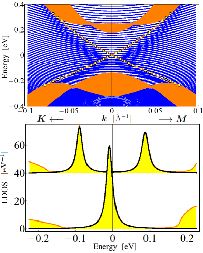
where is the identity matrix and is the unit vector perpendicular to the surface. We note that there is a one-to-one locking between the momentum and the spin, with no out-of-plane spin component. The parameters of the model were determined by the condition that match the tight–binding surface modes (see Fig. 1): eVÅ2, eV, and eVÅ3.
A priori, we can expect that upon coupling to the metal, the spectrum of the surface states will be broadened. This is because even though the spectral profile of the surface states is trivial (i.e., is given by a Dirac function) viewed from the (quasi) two-dimensional point of view, the spectral profile of the metallic states is given by a broad continuous function due to its dependence on the momentum on the direction. Therefore, upon coupling, the surface states will inherit a non-trivial spectral density from the metallic states. Such phenomena have also been observed in particle physics, see, for example Refs. Boyanovsky:2008bf, ; Boyanovsky:2009ke, .
In Eq. (4), the coupling to the metal is captured by the self-energy Z2010a ; Z2010b
| (6) |
where
| (7) |
are the matrix elements of the interaction Hamiltonian between TI surface states and metal states and
| (8) |
is the Green’s function for the metal.
Explicitly carrying out the summation in Eq. (6), we have
| (9) |
with
| (10) |
Here, is the lowest energy of the metal at , is the half–bandwidth at the same wave vector and (i.e., the energy is within the metallic band).
To obtain the matrix , we note that in the vicinity of the point, , the four components of the surface states at the boundary take the form
| (11) |
with the real amplitudes and depending only on and the phase determined by the direction of the wave vector. If, for simplicity, we neglect the dependence on , the coupling becomes diagonal and we have
| (12) |
We conclude that the self–energy in Eq. (4) is proportional to the weight of the surface states at the boundary and to the square of the coupling matrix elements. The real part of the self-energy shifts the surface modes, while the imaginary part broadens the spectrum. This behavior is illustrated in Fig. 1.
In Fig. 1, the upper panel shows the spectrum of a thick TI–metal slab with coupling eV and, for comparison, the spectrum of an uncoupled TI slab, both obtained using the tight-binding model. The energies of the surface states can also be obtained by diagonalizing the effective surface Hamiltonian (5) (small circles in Fig. 1). In the presence of TI-metal coupling, the surface states hybridize with metallic states and do not longer form sharply defined modes. In turn, the spin degeneracy of the metal states is lifted (more on this in the next section). The spectral weight distribution at the interface is shown in the lower panel of Fig. 1. We note the remarkable agreement between the tight–binding (filled lines) and the effective model (black lines) calculations at energies within the bulk TI gap. The positions of the peaks are given by the real parts of the poles of the Green’s function (4), while the widths are given by the imaginary parts. The non–zero local density of states at the boundary generated by bulk TI states can be captured only by the tight–binding approach. We also note that the total weight of an in-gap resonance is independent of the coupling strength, as long as the peak is inside the gap. When the effective coupling is of the order of the gap, the contribution from bulk TI states cannot be neglected and the effective theory is no longer valid.
Before moving on to the case of finite size contacts, we would also like to note that the broadening of the surface modes by the metallic contact has also been observed in a different tight-binding model Zhao:2010fk .
III.2 Finite size contacts
In transport measurements, the size of the contact is finite and thus, translation invariance is broken. Therefore, let us consider the case of a thin contact of length , where is the length of the TI, taken to be finite. The dimensions in the direction are the same. Since translational invariance is broken, momentum in the direction is no longer conserved and the self-energy becomes a matrix in terms of the discrete momentum
| (13) | |||||
where is given by Eq. (9) and the “diffraction” function is given by
| (14) |
The result for the band shift in this case is identical to the translation invariant case, but with rescaled coupling constants,
| (15) |
The peak positions (see Fig. 1) are still given by the real part of the poles of the Green’s function (4), , with the average component. However, the broadening acquires an extra contribution coming from the momentum uncertainty.
This result can be generalized to the case where the contact in the direction is also finite in a straight-forward manner. We conclude that in the case of finite contact, when the size of the metal is negligible compared to the size of the TI, the shift and the broadening of the spectrum of the surface states are negligible.
IV Induced spin texture in semiconductor/topological insulator heterostructures
Let us now consider a TI-semiconductor heterostructure consisting of a thin semiconductor film on top of a thick TI slab. A very thin insulating layer at the interface allows us to control the coupling between the two subsystems. In this work, we consider an “ideal” interface (i.e., we do not include effects due to defects, charged impurities, or lattice mismatch). Our analysis is intended to be a proof of concept in support of the idea that a TI-semiconductor thin film heterostructure can be used for (i) characterizing the TI surface states in the presence of bulk carriers, and (ii) studying the physics of the interface.
The semiconductor film can be described by an effective theory analogous to Eq. (4),
| (16) |
with
| (17) |
where is the coupling matrix element between a semiconductor state with energy and spin and a TI surface state with energy . In a thin film, the semiconductor bands split into subbands indexed by and separated by , where is the effective mass and the film thickness. The semiconductor has to be chosen so that the top valence subband lies within the TI bulk gap. We assume that the uncoupled semiconductor bands are spin degenerate (i.e., the spin-orbit coupling in the semiconductor is negligible). However, when the coupling to the TI is turned on, acquires off-diagonal contributions, or in other words, an effective spin-orbit coupling is induced by the proximity effect.
To understand qualitatively this effect, we focus on the top valence subband and we neglect the inter–band coupling
| (18) |
This becomes exact in the limit , , but our final conclusions are independent of this approximation. Taking into account the form of the surface states at the interface, Eq. (11), the relevant coupling matrix elements are
| (19) |
and , where is the wave function of the semiconductor state at the interface.
The induced spin texture is determined by the structure of the matrix .
Taking into account the properties of the matrix elements we have
| (20) |
As a result, the semiconductor states acquire a spin structure characterized by non-vanishing in-plane spin and zero out-of-plane component. This is a direct consequence of the helical pseudo–spin structure of the TI surface states. In particular, one can also verify that had the surface states had an out-of-plane component, the induced spin would have had an out-of-plane component as well. Therefore, for models with warped Dirac cone, in which away from the point Eq. (11) is no longer valid, out-of-plane pseudo-spin and induced spin components are generated.
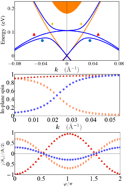
The spin structure of the semiconductor thin film is illustrated in Fig. 2 using a tight-binding calculation for a heterostructure characterized by eV, eV, and . The spin degenerate valence band hybridizes with the TI surface states resulting three coupled modes (upper panel). For a given mode, the value of the in-plane spin (middle panel) is practically equal to the total spectral weight inside the semiconductor. The orientation of the in–plane spin is determined by the momentum direction (bottom panel).
Near the point, the spin structure of the top modes can be described by an effective Rashba-like spin orbit coupling. The effective Rashba coefficient can be read from the effective model and for , it is simplified to
| (21) |
where is the chemical potential and is given by twice of the lattice hopping parameter in the semiconductor.
We note that (i.e., having each pseudo-spin orientation coupled to both spin-up and spin-down) does not induce out-of-plane spin polarization, but rather generates an anisotropic structure characterized by the vanishing of the effective spin-orbit coupling away from the point.
V Conclusions
In this article, we have studied the proximity effects of the interface between TI and metal or semiconductor. The proximity effects cause a shift and broadening of the spectrum of the TI surface states, while lifting spin degeneracy on the metal or semiconductor side. In particular, by probing the induced spin texture in the semiconductor, one can learn about the properties of the TI surface states in more details, even in the excessive presence of the TI bulk carrier. Therefore, we propose a semiconductor thin film/TI heterostructure as a device for studying the properties of the TI surface states.
The induced spin texture can be probed experimentally using, for example, spin-resolved ARPES or STS. Identifying the dispersion of the coupled modes provides direct information about the coupling at the interface. In particular, the strength of the coupling matrix elements can be determined as a function of the thickness of the interface insulating layer. The induced spin texture can also be probed using optical measurements. For optical measurements on Bi2Se3-semiconductor heterostructures, it is convenient to have the conduction band about 1 eV above the valence band, within the energy window characterized by a gap in the TI spectrum at low wave vectors Xia2009 ; Zhang2009 . This will prevent the coupling between the conduction band and the TI, which can generate broadening of the energy levels.
This proposal should complement direct measurement of the spin properties of the surface states such as that found in Ref. Souma:2011uq, and should play a role in resolving the puzzle concerning the spin structure of TIs (see, for example, Ref. Yazyev:2010vn, vs. Ref. Zhang:2010kx, ).
In the present study, we have considered the case of an ideal interface. Future work is required for addressing problems such as the presence of interface defects and impurities, or the effects of the lattice mismatch. These studies of the TI-semiconductor heterostructure will also help understanding key properties of TI-superconductor and TI-ferromagnet interfaces that play a critical role in realizing many of the exotic properties of topological insulators.
Acknowledgements.
We would like to thank our colleagues at WVU, in particular Sergei Urazhdin and Alan Bristow, for their insightful comments. This work is supported in part by West Virginia University start-up funds.References
- (1) C. L. Kane and E. J. Mele, Phys. Rev. Lett. 95, 146802 (2005)
- (2) B. A. Bernevig and S.-C. Zhang, Phys. Rev. Lett. 96, 106802 (2006)
- (3) L. Fu, C. L. Kane, and E. Mele, Phys. Rev. Lett. 98, 106803 (2007)
- (4) L. Fu and C. L. Kane, Phys. Rev. B 76, 045302 (2007)
- (5) J. E. Moore and L. Balents, Phys. Rev. B 75, 121306 (2007)
- (6) R. Roy, Phys. Rev. B 79, 195321 (2009)
- (7) S. Ryu, A. Schnyder, A. Furusaki, and A. Ludwig, New J. Phys. 12, 065010 (2010), 0912.2157, http://arxiv.org/abs/0912.2157
- (8) D. Hsieh, D. Qian, L. Wray, Y. Xia, Y. S. Hor, R. J. Cava, and M. Z. Hasan, Nature 452, 970 (2008)
- (9) Y. Xia, D. Qian, D. Hsieh, L. Wray, A. Pal, H. Lin, A. Bansil, D. Grauer, Y. S. Hor, R. J. Cava, and M. Z. Hasan, Nat. Phys. 5, 398 (2009)
- (10) D. Hsieh, Y. Xia, D. Qian, L. Wray, F. Meier, J. H. Dil, J. Osterwalder, L. Patthey, A. V. Fedorov, H. Lin, A. Bansil, D. Grauer, Y. S. Hor, R. J. Cava, and M. Z. Hasan, Phys. Rev. Lett. 103, 146401 (2009)
- (11) X.-L. Qi, T. L. Hughes, and S.-C. Zhang, Phys. Rev. B 78, 195424 (2008)
- (12) A. M. Essin, J. E. Moore, and D. Vanderbilt, Phys. Rev. Lett. 102, 146805 (2009)
- (13) L. Fu and C. L. Kane, Phys. Rev. Lett. 100, 096407 (2008)
- (14) B. Seradjeh, J. E. Moore, and M. Franz, Phys. Rev. Lett. 103, 066402 (2009)
- (15) X.-L. Qi and S.-C. Zhang(08 2010), 1008.2026v1, http://arxiv.org/abs/1008.2026v1
- (16) M. Z. Hasan and C. L. Kane, Rev. Mod. Phys. 82, 3045 (2010), 1002.3895v2, http://arxiv.org/abs/1002.3895v2
- (17) S. Urazhdin, D. Bilc, S. Tessmer, S. Mahanti, T. Kyratsi, and M. Kanatzidis, Phys. Rev. B 66, 161306(R) (2002)
- (18) P. Roushan, J. Seo, C. V. Parker, Y. S. Hor, D. Hsieh, D. Qian, A. Richardella, M. Z. Hasan, R. J. Cava, and A. Yazdani, Nature 460, 1106 (2009)
- (19) G. D. Mahan, Many Particle Physics, 3rd ed. (Springer, 2000)
- (20) H. Zhang, C.-X. Liu, X.-L. Qi, X. Dai, Z. Fang, and S.-C. Zhang, Nat. Phys. 5, 438 (2009)
- (21) C.-X. Liu, X.-L. Qi, H. Zhang, X. Dai, Z. Fang, and S.-C. Zhang, Phys. Rev. B 82, 045122 (2010), 1005.1682v1
- (22) D. Boyanovsky, R. Holman, and J. A. Hutasoit, Phys. Rev. D79, 085018 (2009), arXiv:0812.4723 [hep-ph]
- (23) D. Boyanovsky, R. Holman, and J. A. Hutasoit, Phys. Rev. D80, 025012 (2009), arXiv:0905.4729 [hep-ph]
- (24) T. D. Stanescu, J. D. Sau, R. M. Lutchyn, and S. Das Sarma, Phys. Rev. B 81, 241310 (2010)
- (25) J. D. Sau, S. Tewari, R. M. Lutchyn, T. D. Stanescu, and S. Das Sarma, Phys. Rev. B 82, 214509 (2010)
- (26) E. Zhao, C. Zhang, and M. Lababidi, Phys. Rev. B, 205331(2010), 1005.3064v2, http://arxiv.org/abs/1005.3064v2
- (27) S. Souma, K. Kosaka, T. Sato, M. Komatsu, A. Takayama, T. Takahashi, M. Kriener, K. Segawa, and Y. Ando, Phys. Rev. Lett. 106, 216803 (2011), 1101.3421v2, http://arxiv.org/abs/1101.3421v2
- (28) O. V. Yazyev, J. E. Moore, and S. G. Louie, Phys. Rev. Lett. 105, 266806 (2010), 1012.1083v1, http://arxiv.org/abs/1012.1083v1
- (29) W. Zhang, R. Yu, H.-J. Zhang, X. Dai, and Z. Fang, New J. Phys. 12, 065013 (2010), 1003.5082v1, http://arxiv.org/abs/1003.5082v1