Electric control of ferromagnetism in Mn-doped semiconductor heterostructures
Abstract
The interplay of tunneling transport and carrier–mediated ferromagnetism in narrow semiconductor multi–quantum well structures containing layers of GaMnAs is investigated within a self-consistent Green’s function approach, accounting for disorder in the Mn–doped regions and unwanted spin–flips at heterointerfaces on phenomenological ground. We find that the magnetization in GaMnAs layers can be controlled by an external electric bias. The underlying mechanism is identified as spin–selective hole tunneling in and out of the Mn-doped quantum wells, whereby the applied bias determines both hole population and spin polarization in these layers. In particular we predict that, near resonance, ferromagnetic order in the Mn doped quantum wells is destroyed. The interplay of both magnetic and transport properties combined with structural design potentially leads to several interrelated physical phenomena, such as dynamic spin filtering, electrical control of magnetization in individual magnetic layers, and, under specific bias conditions, to self–sustained current and magnetization oscillations (magnetic multi-stability). Relevance to recent experimental results is discussed.
pacs:
85.75.Mm, 73.23.Ad, 73.63.-b, 72.25.DcI Introduction
Electric control of magnetism in nanostructures must be viewed as an important milestone on our road map for successful realization of spintronic devices. Although most of the operations in such devices ultimately should be based on spin–only processes, i.e., processes not associated with (highly dissipative) electric charge transport, to gain best benefits from such designs, spin must be manipulated both during the input, control, and read–out stage and eventually be coupled to charge. Several schemes achieving this goal have been explored both at the quantum and semi-classical level, such as the electric distortion of the orbital wave function of spin carriers in inhomogeneous (effective) magnetic fields Shin et al. (2010), electric g-tensor control Roloff et al. (2010); Kroutvar et al. (2004), or spin torque transfer.Myers et al. (1999); Ralph and Stiles (2008); Wenin et al. (2010) Here we explore, on theoretical grounds, the influence of an electric bias on the ferromagnetic state and feasibility of electric control of ferromagnetism in Ga1-x-yAlyMnxAs multiple quantum wells. Structural design, including effective potential profiling and doping to position emitter and collector quasi–Fermi levels, as well as tunneling is used to control hole density and spin polarization within the Mn doped layers.
Dilute magnetic semiconductors (DMS) have been realized by doping of conventional ZnS–structured semiconductors with elements providing open electronic or shells. This has added yet another degree of freedom to the rich spectrum of physical phenomena in semiconductors available for material design with potential for technological applications.Jungwirth et al. (2006) A prominent example is bulk Ga1-xMnxAs where Mn on the Ga sites provides both an open d-shell with a local magnetic moment and a hole which may establish ferromagnetic ordering among the Mn d–electrons, a mechanism known as carrier–mediated ferromagnetism.Ohno et al. (1996); Van Esch et al. (1997); Dietl et al. (2000) The preferentially anti–parallel alignment of the 3/2 spin of the mobile holes with the 5/2 spin of the localized Mn d–electrons promotes ferromagnetic ordering of the latter below a critical temperature of up to K. Theoretical work has confirmed strong hybridization between the 5d Mn and 3p electrons in the ground state.Jain et al. (2001) The effective hole–concentration–dependent exchange field lifts the spin degeneracy of the holes’ energy bands and thus goes hand in hand with hole spin polarization. The Mn ions sitting on Ga sites act as acceptors and are believed to give rise to acceptor levels which lie about 100 meV above the valence band edge.Jungwirth et al. (2006); Van Esch et al. (1997); Schneider et al. (1987) Photoluminescence experiments indicate the co-existence of holes bound to Mn sites and itinerant holes which participate in establishing magnetic order amongst the Mn ions below .Sapega et al. (2009)
Since structural defects of bulk and confined layers of Ga1-xMnxAs depend on grow conditions, Mn concentration , and annealing procedures it is not too surprising that experiments have come up with somewhat different conclusions regarding the “electronic structure of bulk Ga1-xMnxAs”. More recent work seems to hint at the existence of an impurity band which forms at Mn concentrations above 1.5 % leading to a metal–insulator transition in high–quality GaMnAs.Burch et al. (2006); Richardella et al. (2010); Ohya et al. (2011) The Fermi level in these samples is reported to lie in the impurity band and the valence–band properties remain largely GaAs–like.Ohya et al. (2011) The radius of the Mn acceptor wave function has been measured to be about 2 nm, indicating that MnGa is not a shallow acceptor.Richardella et al. (2010) In contrast, other studies rather hint at a disordered top valence band edge containing the Fermi energy, but no isolated impurity band is present.Jungwirth et al. (2006) Recent theoretical work has led to the conclusion that a tight–binding approach (within the coherent-potential approximation for disorder) and local–density functional theory + Hubbard U correction cannot account for an isolated impurity band.Mašek et al. (2010) Other theoretical work has lead to the conclusion that disorder may enhance ferromagnetic stability.Lee et al. (2007); Berciu and Bhatt (2002) Ionized impurity scattering seems to play the dominant role in explaining Hall resistivity data.Yoon et al. (2004)
Controlled growth of heterostructures containing crystalline layers of GaMnAs of high structural quality has remained a challenge up to date. Nevertheless, tunneling spectroscopy has confirmed size quantization effects in GaMnAs quantum well layers.Ohya et al. (2007, 2010a, 2011) However, compared to crystalline GaAs well layers, in an otherwise identical structure, the signature appears to be rather weak and in no sample yet, apparently, has one observed negative differential conductivity due to resonances associated with GaMnAs well layers. This hints at a significant concentration of defects, reminiscent of thin layers of amorphous Si where similar transport studies have revealed size quantization effects but, to our knowledge, not negative differential conductivity.Miyazaki et al. (1987); Li and Pötz (1993) Experimental evidence indicating a coexistence of localized and extended Bloch–like states in bulk GaMnAs, in general, allows the prediction that, in thin layers, certainly for nm, of GaMnAs extended states will be subjected to confinement effects (quantization and energy shifts) while localized states will remain largely unaffected. This is similar to external magnetic–field effects on point defects or quantization effects in amorphous Si.Pötz and Vogl (1983); Li and Pötz (1993) Assuming that no significant additional defects arise in GaMnAs heterostructures, this makes plausible experimental reports on quantum confinement effects arising from (ferromagnetic) GaMnAs layers in thin heterostructures.Ohya et al. (2007, 2010a, 2011) Indeed, when one succeeds to incorporate high–quality magnetic layers in semiconductor heterostructures strongly spin-dependent carrier transmission can be predicted due to spin-selective tunneling.Sankowski et al. (2007) In magnetic resonant tunneling structures of high structural quality this spin splitting may be used for a realization of spin valves, spin filtering, and spin switching devices Likovich et al. (2009); Slobodskyy et al. (2003, 2007); Petukhov et al. (2002); Ohya et al. (2007, 2010b); Ertler and Fabian (2006, 2007), all representing important ingredients for spintronic-based device technology.
In several experiments ferromagnetism has been generated in bulk GaMnAs by, electrically or optically, tailoring the hole density.Ohno et al. (2000); Boukari et al. (2002) In 2d-confined systems containing layers of Ga1-xMnxAs the magnetic order depends strongly on the local spin density, which can be influenced by the tunneling current, resulting in a bias-dependent exchange splitting.Dietl et al. (1997); Jungwirth et al. (1999) A spin-density dependent exchange splitting in ferromagnetic structures enriches the dynamic complexity by offering a mechanism for external electrical control of the ferromagnetic state. This is in contrast to structures comprising paramagnetic DMS, such as ZnMnSe, in which a giant Zeeman splitting of the bands is induced by applying an external magnetic field of the order of a few Tesla.
Already nonmagnetic multi–well heterostructures exhibit interesting dynamic nonlinear effects which are based, however, on different physical mechanisms, such as the formation of electric field domains and the motion of charge dipoles through the structure.Eaves et al. (1989); Pötz (1990); Stegemann and Schöll (2007); Bonilla and Grahn (2005) Recently it has been predicted that, in heterostructures containing paramagnetic DMS wells, this kind of phenomena can be controlled by an external magnetic field.Sánchez et al. (2001); Bonilla et al. (2007); Escobedo et al. (2009) Using an incoherent, sequential tunneling model we have proposed that ferromagnetic multi–well structures can generate ac spin currents, a phenomenon which originates from time–dependent inversion of the spin population in adjacent wells.Ertler et al. (2010)
In this article we investigate spin–selective hole transport in GaAs/AlGaAs/GaMnAs heterostructures within the limit of moderately thin samples with predominantly coherent transport characteristics. We apply a non-equilibrium Green’s function formalism based on a tight–binding Hamiltonian for the electronic structure, including self-consistency regarding the charge density and the exchange splitting of the effective potential, as well as charge transfer to the contacts. Both the carriers’ Coulomb interaction and the exchange coupling with the magnetic ions are described within a mean-field picture. Details of our model are exposed in Sect. II. The mechanism of electric control of magnetization switching is explored for two generic structures containing, respectively, one and two layers of Ga1-xMnxAs. Results are given in Sect. III. We also provide a qualitative explanation for the occurrence of spin-polarized current oscillations, predicted in an earlier paper Ertler et al. (2010), and investigate the influence of spin flip processes at the interfaces on the total current spin polarization. Since disorder seems to play a major role in actual samples we study the effect of substitutional disorder on a qualitative level and discuss the robustness of the effects predicted here. Relevance to experiment is discussed. In particular, we can give an explanation for the absence of exchange splitting (magnetization) under resonance bias condition reported in a recent experiment and identify characteristic features which may be explored in future experiments. Summary and conclusions are given in Sect. IV.
II Physical Model
The magnetic semiconductor heterostructure is described by a two–band tight-binding Hamiltonian for the heavy holes . It is given in the form
| (1) | |||||
where is the spin-dependent () onsite energy at lattice site , denotes the hopping-matrix between neighboring lattice sites, and abbreviates the Hermitian conjugate term. Spin conserving hopping gives a diagonal matrix , whereas spin flip processes can be taken into account by introducing off-diagonal elements. The hopping parameter depends on the effective mass and the lattice spacing between to neighboring lattice sites. The onsite energy
| (2) |
includes the intrinsic hole band profile due to the band offset between different materials, the electrostatic potential with denoting the elementary charge, and the local exchange splitting . Near the band-edges this model is equivalent to an effective–mass model, however, it has the advantage that structural imperfections and spin–flip processes can readily be incorporated. Moreover, it can be extended to arbitrary sophistication by introducing a larger set of basis functions.Sankowski et al. (2007); Schulman and Chang (1983); Pötz (1989a); DiCarlo et al. (1994)
Within a mean-field approach the exchange coupling between holes and magnetic impurities can be described by two interrelated effective magnetic fields, respectively, originating from a nonvanishing mean spin polarization of the ions’ d–electrons and from the hole spin density .Dietl et al. (1997); Jungwirth et al. (1999); Fabian et al. (2007) The exchange splitting of the hole bands is then given by
| (3) |
with being the longitudinal (growth) direction of the structure, is the coupling strength between the impurity spin and the carrier spin density (in case of GaMnAs p-like holes couple to the d-like impurity electrons), and is the impurity density profile of magnetically active ions. Since the magnetic order between the impurities is mediated by the holes, the effective impurity spin polarization depends on the mean hole spin polarization via
| (4) |
where denotes Boltzmann’s constant, is the lattice temperature, and is the Brillouin function of order , here with for the Mn impurity spin. Combining Eq. (3) and Eq. (4) leads to a self-consistent effective Hamiltonian for the holes with
| (5) |
Note that in thermodynamic equilibrium of a quasi 2D-systems, such as a quantum well, the hole spin density polarization is the key figure of merit for the appearance of ferromagnetism.
Within a Hartree mean-field picture space-charge effects are taken into account self-consistently by calculating the electric potential from the Poisson equation,
| (6) |
where denotes the dielectric constant and is the acceptor density. The local hole density at site is given by
| (7) |
with being the in-plane cross sectional area of the structure, and denotes the in-plane momentum. The non-equilibrium “lesser” Green’s function is calculated from the equation of motion
| (8) |
where and denotes the retarded and advanced Green’s function, respectively. The scattering function describes the inflow of particles from the left and right reservoirs Datta (1995)
| (9) |
where is the Fermi distribution function and and , respectively, denote the quasi–Fermi energies in the contacts. The retarded and advanced self-energy terms and account for the coupling of the system region to the left and right semi–infinite chains, for which an analytic expression can be derived.Datta (1995); Economou (1983) The retarded Green’s function is then given by
| (10) |
with being a positive infinitesimal imaginary part of the energy.
Together with adjusting the Fermi energies relative to the band edges in the leads to ensure asymptotic charge neutrality Pötz (1989b), the band splitting given by Eq. (5), the Poisson equation Eq. (6,7), and the kinetic equations Eqs. (8) and (10) have to be solved self-consistently until convergence to a steady–state solution is reached. Nonlinearities in both Hartree and exchange term can give rise to multi–stable behavior, as will be discussed below. If this selfconsistency loop terminates with ferromagnetic ordering in the system, the effective one–particle potential is different for spin–up and spin–down holes, thus leading to spin filtering in transmission.
After obtaining the self-consistent potential profile the spin-dependent transmission probability from the left to the right reservoir, as a matrix element of the structure’s S-matrix, can be calculated from special matrix elements of the retarded Green’s function DiCarlo et al. (1994)
| (11) |
with denoting the free Green’s function of the asymptotic region, and and , respectively, are the spin-dependent group velocities in the leads. is computed most conveniently by adding one layer after another which requires merely 2x2 matrix inversions for the present two–band model.Economou (1983)
Finally, the steady–state current is obtained from scattering theory (generalized Tsu-Esaki formula),
| (12) |
The applied bias is determined by the difference in quasi-Fermi levels of the contacts.
We would like to point out that we conduct a genuine non–equilibrium study whereby the quasi–Fermi level positions are associated with the contacts. Self–consistency then leads to an effective, in general, spin–dependent one–particle potential. Thus one is not confronted with the question where to place the Fermi level in the GaMnAs layers. Essential to confinement effects is the existence of states near the top of the valence band edge of GaMnAs which have a coherence length of at least the layer thickness. Highly localized states, whether separated from or attached to the top valence band edge, will not be very sensitive to finite layer width. While in the bulk and thermal equilibrium the itinerant hole exchange model firmly relates hole density to Tc and the Fermi energy, in a non-equilibrium tunneling situation this is different. The key question is whether tunneling can induce a net hole spin polarization or not. As is shown below, we find that this depends on structural properties as well as on the applied bias.
III Results
We start with a symmetric double–barrier structure containing a single GaMnAs quantum well and investigate the role of resonant hole tunneling on the magnetic state of the device. For the simulation we use generic parameters for GaMnAs and GaAs: , , meV, meV, , , cm-3, eV nm 3 Lee et al. (2000), K, where denotes the free electron mass, is the relative permittivity, is the bare barrier height of AlGaAs relative to GaAs, and , respectively, are the barrier and quantum well width. The thermal equilibrium position of the Fermi energies was deliberately chosen close to the first resonance to promote ferromagnetic ordering in the well region at zero bias. The background charge is assumed to be only about 10% of the Mn doping since GaMnAs is a heavily compensated system, most likely due to Mn interstitial or antisite defects.Van Esch et al. (1997); Das Sarma et al. (2003) The hole densities in the quantum well can be adjusted by the Mn doping level and the quasi-Fermi levels in the contacts. As can be seen from Eq. (5) the exchange splitting increases with the hole density in the case of a steady particle spin polarization. The value of the exchange coupling constant varies in literature to some extend eV nm. Since we use an optimistic value for , we assume only moderate MnGa doping in the well. Higher MnGa densities and smaller values of will give very similar results.
Disorder effects in the GaMnAs layers are modeled by performing a configurational average over structures with randomly selected onsite and hopping matrix elements of the tight-binding Hamiltonian in the Mn doped region. For each specific Hamiltonian the transport problem (I-V curve) is solved self–consistently. The final result is obtained by averaging over all configurations. Typically 300 configurations are used for one I-V curve. For the numerical simulation we assume a fixed 5% Mn concentration in the well and model substitutional disorder. If a Mn ion is present at a given lattice site in the well the onsite energy is shifted according to a Gaussian distribution around a mean onsite energy–shift of 40 meV and a standard deviation of 20 meV, which are reasonable values according to experimental results which indicate either an impurity band slightly above the valence band edge or a defect–induced valence band tail.Ohya et al. (2011); Richardella et al. (2010); Mašek et al. (2010) The nearest–neighbor hopping matrix elements for such a site are sampled according to a Gaussian between 5% and 25% standard deviation () of its bulk value . This model for substitutional disorder leads to a hybridization of quantum confined hole states, associated with bulk like valence band states, and localized defect states arising from MnGa sites. The degree of hybridization depends on layer thickness since it controls the position of the quantized heavy hole band relative to the energy of the localized Mn acceptor levels. This hybridization and the experimentally found Mn acceptor radius of about 2 nm calls for rather thin GaMnAs layers to ensure quantization effects in transport.Ohya et al. (2011)
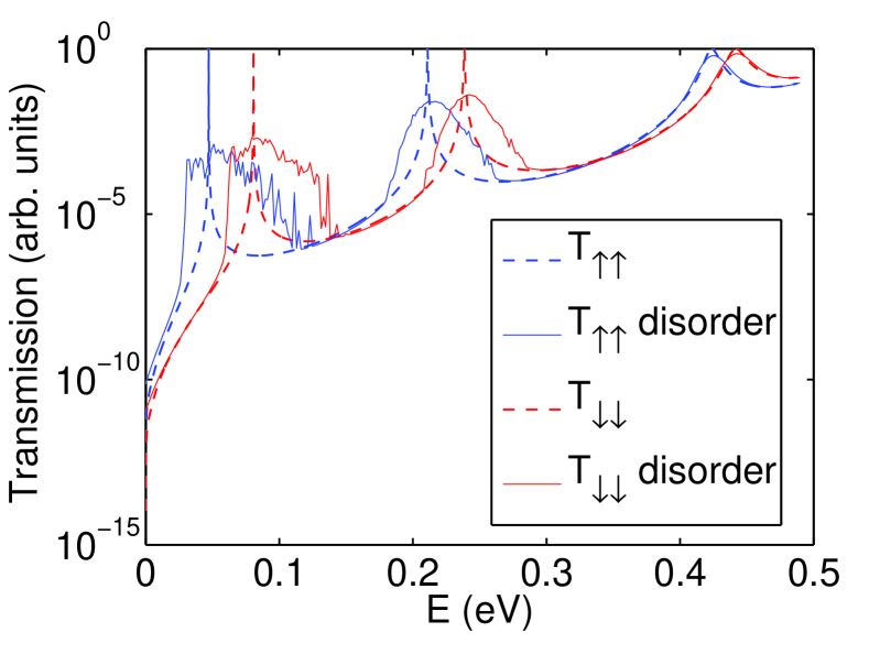
The calculated spin-filtering effect via distinct tunneling probabilities for spin-up and spin-down holes arising from the exchange term is displayed in Fig. 1 in which the transmission probability at zero bias is plotted versus energy of incidence . This figure also gives a qualitative account of the density of states in the GaMnAs well region discussed above. For an idealized GaMnAs layer which, at the valence band edge, is modeled as a GaAs layer plus exchange term, one obtains sharp spin doublets which are exchange–split by about 25-30 meV (see dashed versus solid lines in Fig. 1). The state of zero spin polarization of holes represents an unstable equilibrium since, below Tc, the slightest perturbation in spin–polarization drives the system into a partially ordered lower energy state (spontaneous symmetry breaking) due to the exchange interaction. The latter, in turn, accounts for different effective barrier profiles for spin–up and spin–down holes. It is this nonlinear effect that can be utilized to control the hole spin polarization and thus the favorable Mn spin orientation by structural design and applied bias. Placing the Fermi level near the first heavy–hole resonance promotes this effect, similar to the formation of Cooper pairs near the Fermi edge of an interacting electron gas.
Spin–selective tunneling into and out of the Mn doped wells, regardless of whether sequential or resonant, promotes hole spin polarization and, thus, alignment of the Mn spins as long as spin-depolarizing processes in the heterostructure are slow compared to the effective tunneling rates. Furthermore, disorder which leads to spectral broadening of the resonances may suppress spin–selective tunneling. Inspection of Fig. 1 shows an asymmetric broadening and significant overlap of the transmission peaks under substitutional disorder, modeled as discussed above, which is particularly pronounced for the first heavy–hole resonance since it is most sensitive to potential fluctuations. The asymmetric (“anti–bonding”) shift towards higher energies is due to hybridization with Mn acceptor levels below the conduction band edge. The latter do not contribute to resonant transport. Even at the moderate disorder for the effective hopping matrix element of 5 percent, a significant overlap in spin-up and spin–down resonance is obtained. Increased disorder and/or spin–flip scattering will eventually wash out spin–selectivity in transmission and a destruction of ferromagnetic ordering under bias must be expected since unpolarized holes are steadily fed into the GaMnAs regions. Exchange splitting at zero bias for 5% and 25%, respectively, is reduced to 33 meV and 23 meV.
Clearly, our effective one–dimensional modeling of (substitutional) disorder must be viewed as a limited estimate since it corresponds to a cross–sectional average of transport though uncorrelated effective linear chains. Correlations from disorder parallel to the heterointerface will play a role in the establishing of coherence and ferromagnetic order in real structures relative to the idealized homogeneous mean–field model adopted here, since both ferromagnetic order and disorder effects are highly dependent upon spatial dimensionality.Kaxiras (2003); Ashcroft and Mermin (1976) Additional types of disorder from Mn clustering, Mn interstitials, etc. may be present in real structures. The role of disorder in the formation of ferromagnetic order in diluted magnetic semiconductors has been explored theoretically and, remarkably, certain form of disorder has been predicted to promote ferromagnetic ordering.Lee et al. (2007); Berciu and Bhatt (2002) In experiment, STM studies have given information on the nature of defects near the surface of GaMnAs samples.Burch et al. (2006); Richardella et al. (2010)
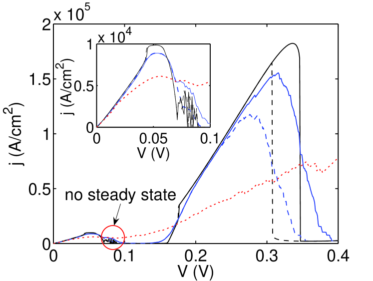
The current-voltage I–V characteristics, plotted in Fig. 2, reveals the typical hysteretic behavior of resonant tunneling diodes for an up- and down-sweep of the applied bias. This well known intrinsic bistability occurs due to different charging of the well depending on the bias–sweep direction. Since our model ignores contributions from the light–hole band, associated resonances are missing in the plot. The latter are important due to in–plane non–parabolicity effects in narrow layers, however, low–lying resonances associated with heavy and light holes generally are clearly separated in energy. For the present structure a light–hole–band resonance would be expected between the first two heavy–hole–associated resonances, thus strongly reducing the peak–to valley ratio and contributing spin holes to the Mn–doped layers. It should be observed that only single resonance peaks are observed in the I–V characteristics in spite of spin doubles in the (zero–bias) transmission spectra. Furthermore, the drop in current beyond the first heavy–hole peak value (see insert in Fig. 2), unlike in ballistic models for nonmagnetic tunneling structures (see second peak), is gradual even in the absence of disorder. This broadening of the resonance can be attributed to ferromagnetic ordering away from the first resonance peak which tends to widen the bias window for meeting the resonance condition.
Disorder effects diminish the peak–to valley ratio but regions of negative differential resistance are maintained for weak disorder. Since experiments have not shown negative differential conductivity in such a structure we have increasing disorder and find its disappearance at relatively high hopping disorder of about % (see Fig. 2). This indicates that defects other than Mn acceptors are present in real samples. Further numerical studies regarding this issue will be published elsewhere.Ertler and Pötz (2011)
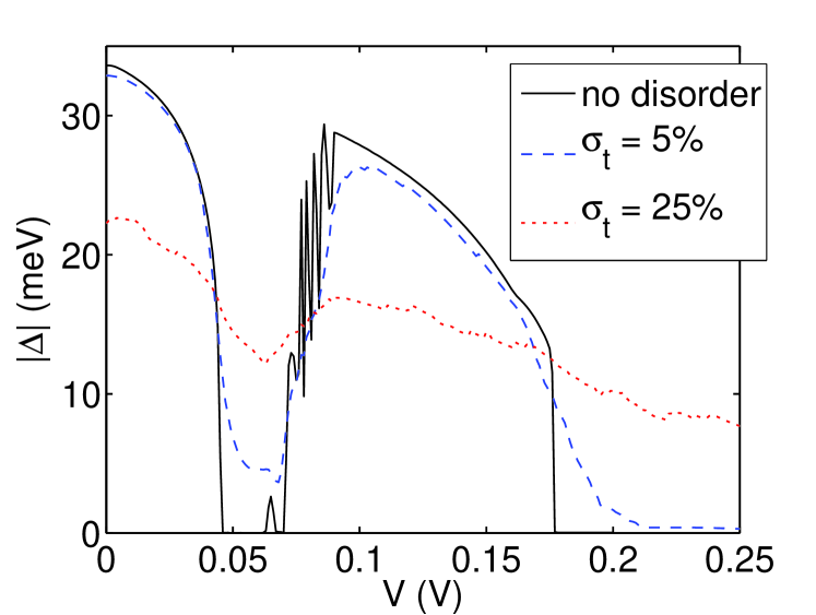
In Fig. 3 the average exchange band spin splitting in the quantum well, characterizing its magnetic state, is plotted versus applied bias. It shows that ferromagnetism can be controlled by the applied bias in this structure near the first current peak, remarkably, even when disorder is sufficiently strong to suppress negative differential conductivity. At zero bias ferromagnetic ordering is energetically preferred since the Fermi level is located close to the edge of the first heavy–hole subband. As the bias is increased tunneling into the upper doublet state becomes allowed from the emitter side reducing the net hole–spin polarization (in spite of increasing hole density) and the effective exchange field decreases to zero and both spin–up and spin–down subbands go into resonance. Note that under moderate bias both emitter and collector contribute to the population of the well region. As the bias increases resonant population from the emitter gets shut off and hole polarization is determined by the collector leading once more to a build-up of the exchange field for a bias regime between 0.08 V and 0.2 V, when finally the collector quasi-Fermi level drops below the hole subbands and the well region becomes almost depleted of holes. For higher bias no further spontaneous magnetization has been obtained within our self–consistency loop. The overall feature of the bias dependence of the exchange splitting thus somewhat resembles its behavior versus temperature, with “” corresponding to a bias of about 0.18 V. It arises from the fact that it is the number of spin–polarized holes which determines the maximum spontaneous magnetization for given Mn concentration. A simple model for the dependence of the Curie temperature in resonant tunneling systems has been given by one of us before.Ertler (2008) The voltage-dependence of the Curie temperature under resonant tunneling has also been studied before.Ganguly et al. (2005)
The displayed build–up and destruction of ferromagnetic order as a function of applied bias can be further understood by the exchange interaction which is mediated by spin–polarized holes. In an ideal 2D particle system with parabolic dispersion there is no energy gain by magnetic ordering due to the constant density of states associated with each spin subband: energy gained by lowering one subband is exactly cancelled by raising the other. However, here we deal with a 3D heterostructure which favors a spin ordered state when the quasi–Fermi level lies near (within about half of the maximal exchange splitting) the bottom of a well subband resonance. If the temperature in the contacts is sufficiently low, one subband after the other will go through resonance. Thus, when only the lower spin–subband is in resonance holes in the magnetic well will tend to be be spin–polarized. However, as bias is increased eventually the subband with opposite spin orientation will also go into resonance thus reducing spin polarization and magnetic ordering in the GaMnAs layer. When, for a given bias, the well region cannot be populated (lack of hole density of states) or no energy gain can be drawn from ferromagnetic ordering, loss of the latter will result.
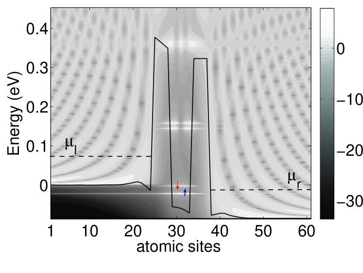
Interestingly, in the voltage range of V no steady state solution can be found for the low disorder sample case. Instead the solution for the magnetization is oscillating, as shown in Fig. 3, suggesting the occurrence of dynamic effects. This behavior can be understood qualitatively as follows: Figure 5 shows a contour plot of the local density of states, for an applied bias V lying in the critical voltage range. The self–consistent band profile is indicated by the solid line. For the emitter Fermi energy of eV only the two ground state (potentially spin–split) subbands in the quantum well participate in the tunneling transport. At this bias condition and hole spin polarization the lowest (spin–up) subband may be populated by holes from the collector side, whereas the spin–down level is almost empty since it cannot be reached elastically by either emitter or collector. Since the (steady–state) band splitting is proportional to the spin polarization the well magnetization increases with spin polarization, pushing the spin–down level upwards in energy. At some point holes can start to tunnel from the emitter side into the spin–down level. This in turn decreases the total spin polarization and, hence, effectively pushes the spin–down level back below the emitter’s band edge. From there, the process starts anew, leading to an oscillatory behavior in well magnetization, tunneling current, and spin polarization.Ertler et al. (2010)
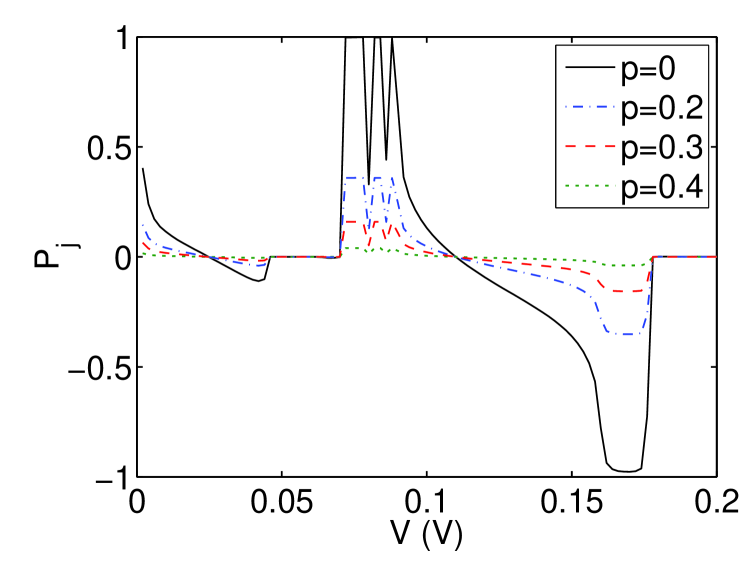
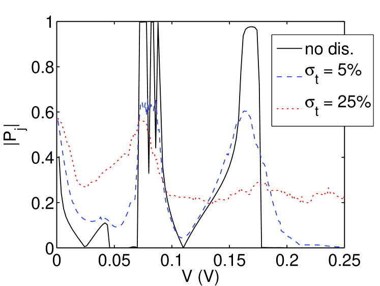
Although the I-V curves in Fig. 2 do not display spin-split resonance peaks, but merely a broadening of the resonance, the steady–state current at low bias is spin polarized as shown in Fig. 4. As the bias is increased from zero, current spin polarization is reduced and reversed before it drops to zero through resonance. Above resonance current spin polarization reemerges (due to the action of the collector) and once more changes sign before dropping and remaining at zero in one-to-one agreement with the behavior of the exchange field. Although resonance peaks in the I-V curve my be suppressed by disorder, see Fig. 2, the bias–dependence of spin polarization in the current may persist and may be observed in experiment as a bias–dependent spin valve.
In order to study qualitatively the influence of spin flip processes at the hetero–interfaces on the total current spin polarization at the collector side, with , we introduce off-diagonal hopping matrices in the tight-binding Hamiltonian. In general for interfaces there are different flip configurations. For each of them a simulation is performed and the results are finally averaged by weighting with the probability for the occurrence of the configuration. In the case of a double-barrier structure we have four hetero-interfaces, giving configurations. However, flipping at the first barrier interfaces is inefficient, since it does not change the total current or spin polarization. Single flipping at the third or fourth interface does also not modify the total current density but inverts the spin polarization to . By introducing single spin flip probabilities at the interface , the probability of a flipping process at the second barrier is then given by . Hence, the mean spin polarization results in
| (13) |
The bias-dependent current spin polarization for different spin flip probabilities (assuming ) is plotted in Fig. 6. The spin polarization decreases for increasing with reaching its minimum for . From this analysis we conclude that our results will not be altered significantly when the spin–orbit interaction is taken into account in the analysis.
While spin–selective hole tunneling may allow electric control of ferromagnetic order, tunneling spectroscopy, in turn, provides a sensitive experimental tool for exploring the electronic structure of mesoscopic semiconductor systems.Smoliner (1996) Recently, tunneling spectroscopy experiments have been performed on thin layers of GaMnAs.Ohya et al. (2011) The authors have verified ferromagnetic ordering in their samples (with Mn concentration of typically 5 to 15 and layer thickness ranging from 4 to 20 nm) and have measured their respective Curie temperature. Their measurements indicate that Mn induced defect states remain separated from the GaAs–like valence band edge as evidenced by a pinning of the Fermi level. Furthermore, they find clear signatures of quantization effects in the transmission spectra of their samples and report an absence of spin-splitting in the resonances which they can fit to a GaAs-like k.p model, including light-hole states. We believe that these experimental findings compare favorably with the general features of our results. Moreover, we have provided an explanation for the observed absence of ferromagnetic ordering near resonance in spite of ferromagnetic behavior of the sample at zero bias. It would be interesting to perform spin–sensitive tunneling spectroscopy on these samples since, according to Fig. 6, such a measurement gives more detailed information about the bias dependence of ferromagnetic ordering than the I-V curve and its derivatives. This can test the prediction that ferromagnetic order which can be achieved at zero bias is destroyed near resonance would be verified, and that electric switching back and forth between the ferromagnetic and paramagnetic state can be achieved.
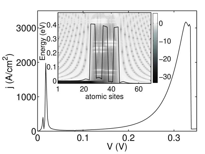
We now explore feasibility of selective magnetization switching among several magnetic layers of high structural quality. We investigate a three-barrier structure with two adjacent GaMnAs quantum wells, choosing an asymmetric structure with the second well being thinner than the first one (, ). All other parameters are as in the previous structure. Quantum confinement gives rise to a higher ground state energy in the second quantum well at zero bias. The resonant alignment of the ground state subbands of the two wells is therefore achieved at a finite voltage as shown in the inset of Fig. 7, corresponding to the first maximum in the current-voltage characteristics at about V which is plotted in Fig. 7. The second current maximum result from the resonance of the first excited state subbands of both wells. Next to possible exchange splitting the finite separating barriers cause the energy levels in the two quantum wells to further split into bonding and antibonding subband states. However, for our structure the middle barrier is too thick and the natural energy broadening of the quasi–bound states is too large for resolving this additional splitting in the local density of states.
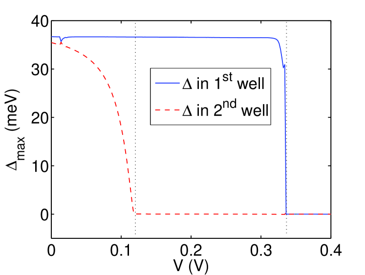
Having two coupled quantum wells allows one to realize several magnetic configurations. The maximum (steady–state) exchange splitting of the two wells as a function of the applied bias is plotted in Fig. 8, revealing three different regions. For low voltages both wells are magnetized due to the build–up of spin polarization in the wells due to resonance of the ground state subband levels with populated reservoir states. Exchange causes a relative shift in the density of states for spin–up and spin–down holes which, in turn, stabilizes ferromagnetism in both layers. When the second well goes off resonance at around V the accumulated spin polarization in the second well is preserved, since for voltages up to V the collector Fermi energy is still higher than the bottom of its ground state subbands thus maintaining spin polarization. For voltages in the interval V V the first well remains magnetic, whereas the second well becomes nonmagnetic, since the ground state subbands are no longer filled from the collector side. At sufficiently high bias, V, also the first well becomes demagnetized since holes can no longer resonantly populate its two lowest (now degenerate) subbands from either emitter or collector thus resulting in a completely nonmagnetic structure.
Several simplifying assumptions have been made in the present analysis which should, just as well as experimental aspects, be discussed. The present model is based on an effective-mass-like two–band approach for the heavy holes in the structure. This approximation should at least qualitatively be correct since the applied bias is kept below typically 0.2 V and most of the phenomena discussed here occur at lower bias. Thus it can be expected, that this model describes effects qualitatively correct. We are currently working on more realistic tight–binding formulations using a significantly increased number of basis states in conjunction with density functional plus dynamic mean-field models to arrive at a more detailed and realistic electronic structure.Chioncel et al. (2011) Impurity scattering effects have been accounted for on a phenomenological level within the TB model. Our ballistic model neglects electron–phonon scattering within the heterostructure altogether and the electron–electron interaction is described within mean–field theory. In thin structures, such as the ones studied here where effective tunneling rates are higher than carrier–phonon scattering rates and optical phonon transitions are suppressed energetically the former assumption should be rather well fulfilled and not alter significantly subband population within the heterostructure. Electron–electron scattering may play role, however, as long as it does not involve spin–flip processes should not influence our basic conclusions much.
Clearly the effects studied here require low temperatures, for one to favor ferromagnetic ordering and, secondly, to preserve strong hole–spin polarization in the carrier injection process. It is well known that, at least at low temperatures, structural imperfections are the main source for reduction of nonlinear effects, such as the peak–to–valley–ratio in the IV curve.Pötz (1989a); Pötz and Li (1989); Chevoir and Vinter (1990); Mizuta and Tanoue (1995) It is most likely the difficulty in clean sample preparation which has slowed experimental progress on thin–layer semimagnetic semiconductor heterostructures. High quality doping profiles and high quality interfaces must be achieved within one growth process.Ohya et al. (2007); Likovich et al. (2009); Ohya et al. (2010b) Growth of good quality DMS layers needs low temperature molecular beam epitaxy which, however, adversely affects interface quality. Usually thin GaAs spacer layers are inserted to smooth the surfaces.Ohya et al. (2007, 2010b) Furthermore, GaMnAs layers must be thick enough to support ferromagnetism. Qualitatively, all structural imperfections lead to broadening of resonances. Once the latter becomes comparable to the (theoretical) maximum of the exchange energy induced spin–splitting, spin–selective tunneling and, hence, tunneling–induced control of magnetic ordering may be suppressed. Even in the presence of disorder, as long as it does not go hand in hand with strong spin–flip processes, achieving bias–control of hole–spin polarization in the GaMnAs layers should allow one to manipulate magnetization.
IV Conclusions and Outlook
In summary, we have used a ballistic steady–state transport model to investigate bias–induced magnetic multi–stability in AlGaAs/MnGaAs quantum well structures. Ferromagnetic exchange, as well as the hole Coulomb interaction are treated within self–consistent mean–field approximation. Substitutional disorder is treated phenomenologically within a tight–binding model.
Our studies indicate that in these systems ferromagnetic ordering can be controlled selectively by an externally applied bias. The underlying mechanism is found in spin–selective tunneling due to the anti–ferromagnetic exchange interaction between itinerant heavy holes and localized Mn d–electrons. In structurally suitably designed heterostructures the applied electric bias allows control of the ferromagnetic state, as well as electric and spin current density.
In the simplest structural case in form of a double barrier structure containing a GaMnAs well, we predict that ferromagnetic ordering in the well, when present at zero bias, is lost under bias near the first heavy-hole resonance, allowing a switching back and forth between the magnetic and nonmagnetic state in the well. In GaMnAs multi-well structures we predict that the loss of ferromagnetic order can be engineered structurally to occur at different applied bias for the individual layers.
Within our model we are able to provide a possible explanation for the absence of exchange splitting near resonances, as observed in recent tunneling spectroscopy measurements on thin GaMnAs layers.Ohya et al. (2011) We generally predict that ferromagnetic order which may be achieved in GaMnAs quantum well layers under zero bias tends to be destroyed under resonance condition since the well region then is swept by unpolarized holes. Under favorable conditions detailed in the main text, ferromagnetic order may be reestablished above resonance. Such a behavior should be revealed experimentally by spin–sensitive tunneling spectroscopy.Ando et al. (2005)
In previous work based on a complementary time–dependent sequential tunneling model including intra–well scattering we have predicted that, under specific bias conditions, the interplay of transport and magnetic properties can result in robust self-sustained charge and magnetization oscillations.Ertler et al. (2010) The present model, albeit based on the resonant–tunneling picture, backs the possibility of such phenomena by predicting bias regions in which no steady–state solution for the current exists.
Disorder and spin–flip effects have been modeled on a phenomenological level. We find that disorder due to Mn taking a Ga site alone should not suffice to destroy spin–selective tunneling, nor should spin flips at a rate expected in these structures, for example from the spin–orbit interaction, significantly suppress spin polarization of the steady–state current. As expected, our analysis does show that disorder and spin flip processes do reduce the total average current spin polarization, however, not as efficiently as the resonance peaks in the I–V curve.
We conclude that multi–well structures containing GaMnAs layers may allow one to realize various bias-dependent magnetic configurations. While the current investigation of bias induced effects considers only bias in longitudinal direction, i.e., a 2–terminal configuration, applying additional gates in transverse direction (multi–terminal configuration) should allow for an additional control knob to move spin–split subbands in and out of resonance with the contact states and/or to inject spin–polarized holes into the Mn–doped regions. Such a structure has been studied in a recent experiment.Ohya et al. (2010b)
V Acknowledgment
This work has been supported by the FWF project P21289-N16.
References
- Shin et al. (2010) Y.-S. Shin, T. Obata, Y. Tokura, M. Pioro-Ladrière, R. Brunner, T. Kubo, K. Yoshida, and S. Tarucha, Phys. Rev. Lett. 104, 046802 (2010).
- Roloff et al. (2010) R. Roloff, T. Eissfeller, P. Vogl, and W. Pötz, New J. Phys. 12, 093012 (2010).
- Kroutvar et al. (2004) M. Kroutvar, Y. Ducommun, D. Heiss, M. Bichler, D. Schuh, G. Absteiter, and J. J. Finley, Nature 432, 81 (2004).
- Myers et al. (1999) E. B. Myers, D. C. Ralph, J. A. Katine, R. N. Louie, and R. Buhrman, Science 285, 867 (1999).
- Ralph and Stiles (2008) D. C. Ralph and M. D. Stiles, J. Magn. Magn. Mat. 320, 1190 (2008).
- Wenin et al. (2010) M. Wenin, A. Windisch, and W. Pötz, J. Appl. Phys. 108, 103717 (2010).
- Jungwirth et al. (2006) T. Jungwirth, J. Sinova, J. Mašek, J. Kučera, and A. H. MacDonald, Rev. Mod. Phys. 78, 809 (2006).
- Ohno et al. (1996) H. Ohno, A. Shen, F. Matsukura, A. Oiwa, A. End, S. Katsumoto, and Y. Iye, Appl. Phys. Lett. 69, 363 (1996).
- Van Esch et al. (1997) A. Van Esch, L. Van Bockstal, J. De Boeck, G. Verbanck, A. S. van Steenbergen, P. J. Wellmann, B. Grietens, R. Bogaerts, F. Herlach, and G. Borghs, Phys. Rev. B 56, 13103 (1997).
- Dietl et al. (2000) T. Dietl, H. Ohno, F. Matsukura, J. Cibert, and D. Ferrand, Science 287, 1019 (2000).
- Jain et al. (2001) M. Jain, L. Kronik, J. R. Chelikowsky, and V. V. Godlevsky, Phys. Rev. B 64, 245205 (2001).
- Schneider et al. (1987) J. Schneider, U. Kaufmann, W. Wilkening, M. Baeumler, and F. Köhl, Phys. Rev. Lett. 59, 240 (1987).
- Sapega et al. (2009) V. F. Sapega, N. I. Sablina, I. E. Panaiotti, N. S. Averkiev, and K. H. Ploog, Phys. Rev. B 80, 041202(R) (2009).
- Burch et al. (2006) K. S. Burch, D. B. Shrekenhamer, E. J. Singley, J. Stephens, B. L. Sheu, R. K. Kawakami, P. Schiffer, N. Samarth, D. D. Awschalom, and D. N. Basov, Phys. Rev. Lett. 97, 87208 (2006).
- Richardella et al. (2010) A. Richardella, P. Roushan, S. Mack, B. Zhou, D. A. Huse, D. D. Awschalom, and A. Yazdani, Science 327, 665 (2010).
- Ohya et al. (2011) S. Ohya, K. Takata, and M. Tanaka, Nature Physics 7, 342 (2011).
- Mašek et al. (2010) J. Mašek, F. Máca, J. Kudrnovský, O. Makarovsky, L. Eaves, R. P. Campion, K. W. Edmonds, A. W. Rushforth, C. T. Foxon, B. L. Gallagher, et al., Phys. Rev. Lett. 105, 227202 (2010).
- Lee et al. (2007) B. Lee, X. Cartoixà, N. Trivedi, and R. M. Martin, Phys. Rev. B 76, 155208 (2007).
- Berciu and Bhatt (2002) M. Berciu and R. N. Bhatt, Physica B 312, 815 (2002).
- Yoon et al. (2004) I. T. Yoon, T. W. Kang, K. H. Kim, and D. J. Kim, J. Appl. Phys. 95, 3607 (2004).
- Ohya et al. (2007) S. Ohya, P. N. Hai, Y. Mizuno, and M. Tanaka, Phys. Rev. B 75, 155328 (2007).
- Ohya et al. (2010a) S. Ohya, I. Muneta, P. N. Hai, and M. Tanaka, Phys. Rev. Lett. 104, 167204 (2010a).
- Miyazaki et al. (1987) S. Miyazaki, Y. Ihara, and M. Hirose, Phys. Rev. Lett. 59, 125 (1987).
- Li and Pötz (1993) Z. Q. Li and W. Pötz, Phys. Rev. B 47, 6509 (1993).
- Pötz and Vogl (1983) W. Pötz and P. Vogl, Solid State Commun. 48, 249 (1983).
- Sankowski et al. (2007) P. Sankowski, P. Kacman, J. A. Majewski, and T. Dietl, Phys. Rev. B 75, 45306 (2007).
- Likovich et al. (2009) E. Likovich, K. Russell, W. Yi, V. Narayanamurti, K.-C. Ku, M. Zhu, and N. Samarth, Phys. Rev. B 80, 201307(R) (2009).
- Slobodskyy et al. (2003) A. Slobodskyy, C. Gould, T. Slobodskyy, C. R. Becker, G. Schmidt, and L. W. Molenkamp, Phys. Rev. Lett. 90, 246601 (2003).
- Slobodskyy et al. (2007) A. Slobodskyy, C. Gould, T. Slobodskyy, G. Schmidt, L. W. Molenkamp, and D. Sánchez, Appl. Phys. Lett. 90, 122109 (2007).
- Petukhov et al. (2002) A. G. Petukhov, A. N. Chantis, and D. O. Demchenko, Phys. Rev. Lett. 89, 107205 (2002).
- Ohya et al. (2010b) S. Ohya, I. Muneta, and M. Tanaka, Appl. Phys. Lett. 96, 052505 (2010b).
- Ertler and Fabian (2006) C. Ertler and J. Fabian, Appl. Phys. Lett. 89, 242101 (2006).
- Ertler and Fabian (2007) C. Ertler and J. Fabian, Phys. Rev. B 75, 195323 (2007).
- Ohno et al. (2000) H. Ohno, D. Chiba, F. Matsukura, T. O. E. Abe, T. Dietl, Y. Ohno, and K. Ohtani, Nature 408, 944 (2000).
- Boukari et al. (2002) H. Boukari, P. Kossacki, M. Bertolini, D. Ferrand, J. Cibert, S. Tatarenko, A. Wasiela, J. A. Gaj, and T. Dietl, Phys. Rev. Lett. 88, 207204 (2002).
- Dietl et al. (1997) T. Dietl, A. Haury, and Y. M. d’Aubigné, Phys. Rev. B 55, R3347 (1997).
- Jungwirth et al. (1999) T. Jungwirth, W. A. Atkinson, B. H. Lee, and A. H. MacDonald, Phys. Rev. B 59, 9818 (1999).
- Eaves et al. (1989) L. Eaves, M. L. Leadbeater, D. G. Hayes, E. S. Alves, F. W. Sheard, G. A. Toombs, P. E. Simmonds, M. S. Skolnick, M. Henini, and O. H. Hughes, Solid State Electr. 32, 1101 (1989).
- Pötz (1990) W. Pötz, Phys. Rev. B 41, 12111 (1990).
- Stegemann and Schöll (2007) G. Stegemann and E. Schöll, New J. Phys. 9, 55 (2007).
- Bonilla and Grahn (2005) L. L. Bonilla and H. T. Grahn, Rep. Prog. Phys. 68, 577 (2005).
- Sánchez et al. (2001) D. Sánchez, A. H. MacDonald, and G. Platero, Phys. Rev. B 65, 035301 (2001).
- Bonilla et al. (2007) L. L. Bonilla, R. Escobedo, M. Carretero, and G. Platero, Appl. Phys. Lett. 91, 092102 (2007).
- Escobedo et al. (2009) R. Escobedo, M. Carretero, L. L. Bonilla, and G. Platero, Phys. Rev. B 80, 155202 (2009).
- Ertler et al. (2010) C. Ertler, W. Pötz, and J. Fabian, Appl. Phys. Lett. 97, 042104 (2010).
- Schulman and Chang (1983) J. N. Schulman and Y.-C. Chang, Phys. Rev. B 27, 2346 (1983).
- Pötz (1989a) W. Pötz, Superlatt. Microstruct. 6, 187 (1989a).
- DiCarlo et al. (1994) A. DiCarlo, P. Vogl, and W. Pötz, Phys. Rev. B 50, 8358 (1994).
- Fabian et al. (2007) J. Fabian, A. Matos-Abiague, C. Ertler, P. Stano, and I. Žutić, Acta Physica Slovaca 57, 565 (2007).
- Datta (1995) S. Datta, Electronic Transport in Mesoscopic Systems (Cambridge University Press, Cambridge, England, 1995).
- Economou (1983) E. N. Economou, Green’s Functions in Quantum Physics (Springer, Berlin, 1983).
- Pötz (1989b) W. Pötz, J. Appl. Phys. 66, 2458 (1989b).
- Lee et al. (2000) B. Lee, T. Jungwirth, and A. H. MacDonald, Phys. Rev. B 61, 15606 (2000).
- Das Sarma et al. (2003) S. Das Sarma, E. H. Hwang, and A. Kaminski, Phys. Rev. B 67, 155201 (2003).
- Kaxiras (2003) E. Kaxiras, Atomic and Electronic Structure of Solids (Cambridge University Press, Cambridge, 2003).
- Ashcroft and Mermin (1976) N. W. Ashcroft and N. D. Mermin, Solid State Physics (Saunders, Philadelphia, 1976).
- Ertler and Pötz (2011) C. Ertler and W. Pötz, submitted to J. Comp. Elec. (2011).
- Ertler (2008) C. Ertler, Appl. Phys. Lett. 93, 142104 (2008).
- Ganguly et al. (2005) S. Ganguly, L. F. Register, S. Banerjee, and A. H. MacDonald, Phys. Rev. B 71, 245306 (2005).
- Smoliner (1996) J. Smoliner, Semicond. Sci. Technol. 11, 1 (1996).
- Chioncel et al. (2011) L. Chioncel, I. Leonov, H. Allmaier, F. Beiuşeanu, E. Arrigoni, T. Jurcuţ, and W. Pötz, Phys. Rev. B 83, 035307 (2011).
- Pötz and Li (1989) W. Pötz and Z. Q. Li, Solid State Electr. 32, 1353 (1989).
- Chevoir and Vinter (1990) F. Chevoir and B. Vinter, Surf. Sci. 229, 158 (1990).
- Mizuta and Tanoue (1995) H. Mizuta and T. Tanoue, The Physics and Applications of Resonant Tunneling Diodes (Cambridge University Press, Cambridge, 1995).
- Ando et al. (2005) Y. Ando, T. Miyakoshi, M. Oogane, and T. Miyazaki, Appl. Phys. Lett. 87, 142502 (2005).