Atomistic simulations of the implantation of low energy boron and nitrogen ions into graphene
Abstract
By combining classical molecular dynamics simulations and density functional theory total energy calculations, we study the possibility of doping graphene with B/N atoms using low-energy ion irradiation. Our simulations show that the optimum irradiation energy is 50 eV with substitution probabilities of 55% for N and 40% for B. We further estimate probabilities for different defect configurations to appear under B/N ion irradiation. We analyze the processes responsible for defect production and report an effective swift chemical sputtering mechanism for N irradiation at low energies (125 eV) which leads to production of single vacancies. Our results show that ion irradiation is a promising method for creating hybrid C-B/N structures for future applications in the realm of nanoelectronics.
pacs:
81.05.ue, 61.72.U-, 83.10.MjI Introduction
Graphene Novoselov2004 is a two-dimensional all-carbon nanostructure consisting of -bonded carbon atoms arranged in a honeycomb-like lattice. Similar to carbon nanotubes Iijima1991 , which can be imagined as graphene sheets rolled up to form seamless tubes, it has attracted a considerable amount of attention, especially due to its unique electronic properties CastroNeto2009 . Pristine graphene is a zero band gap material with a high electron mobility, but introduction of impurities and structural defects CastroNeto2009 ; Appelhans2010 can lead to band gap opening and Fermi level shifting. This makes graphene an interesting candidate for many applications in nanoelectronics. However, despite recent breakthroughs in graphene production Li05062009 ; Bae10nn , one of the remaining problems on the way towards graphene-based electronic devices is the lack of control over the electronic properties of the as-grown samples.
In today’s semiconductor industry, a standard way to modify the electronic properties of a material is doping with foreign atom species. For an all-carbon material, such as graphene, the natural dopants are boron and nitrogen, which posses one electron less and more than carbon, respectively. Since they are also roughly similar in size to carbon, they can be incorporated into substitutional positions in carbon structures by replacing exactly one carbon atom, or take the vacant site at the edges of graphene flakes Yan2007 ; Huang2007 ; Reddy10acs ; Wang09sci ; Wei09nlD . It has been shown Late2010 than B/N-doped graphene displays /-type behavior. Not surprisingly, several theoretical studies on hybrid C-B/N systems Zheng2008 ; Lherbier2008 ; Peres2007 ; Zheng2010a ; Yu2010b ; Wang2010b have recently been carried out. Particular attention has been paid to graphene nanoribbons Zheng2009a ; Pekoz2009 ; Biel2009 ; Yu2010 ; Yu2010a ; Huang2010 . Although it is possible to introduce B/N atoms into graphene during synthesis Reddy10acs ; Wang09sci ; Wei09nlD ; Ozaki2007 ; Lin2009 ; Ci2010 ; Raidongia2010 , not many studies have investigated the possibility of selectively introducing B/N impurities into graphene after growth, while post-synthesis doping may be an alternative way to create graphene-based functional materials. It was demonstrated in a recent study that B can be incorporated into graphene structure by selectively exposing different sides of a graphene monolayer to different atomic environments Pontes2009 . Unfortunately, it is not clear how this could be carried out in practice. While ion irradiation is routinely used nowadays when manufacturing conventional semi-conductor devices, one can expect that it can be used in a similar manner to introduce B/N atoms into graphene. However, graphene, an atomically thin target, has a significantly different response to ion irradiation as compared to traditional three-dimensional materials Lehtinen2010 . In a recent experimental study Guo2010 , N+ ion irradiation was used to facilitate N-doping of graphene. Due to a high irradiation energy (30 keV), very few if any ions were directly incorporated to the graphene sheet. Instead, the nitrogen atoms were later introduced during annealing in a NH3 atmosphere. Clearly, the optimization of the implantation process requires full microscopic understanding of the response of graphene to ion irradiation.
In this study, we employ classical molecular dynamics (MD) simulations and density functional theory (DFT) total energy calculations to study the efficiency of ion beam doping of graphene as a function of ion energy. We show that at energies close to 50 eV, it is possible to incorporate as much as 55% of N and almost 40% of B impinging ions to the substitutional dopant site in graphene. The most typical defects which appear under low energy irradiation include single and double vacancies. In the preferred range of doping energies, the probability for introducing additional defects to graphene during ion beam doping remains below 37%. We also report a swift chemical sputtering mechanism (especially for N ions) for ion energies below 150 eV, which along with the ballistic knock-out, leads to production of single vacancies. This effect may have an important role in defect creation during experimental ion beam doping of graphene, and possibly other carbon materials.
II Methods
To study B/N ion implantation into graphene, we followed the same approach as in our earlier work on ion irradiation of carbon nanotubes Kotakoski2005 ; Kotakoski2005a ; Tolvanen2007 ; Kra05chan and graphene Lehtinen2010 . The interactions between the atoms in the system under study were described by the bond order potentials developed by Matsunaga et al. Matsunaga1999 for C-B/N and by Brenner et al. Brenner1990 for C-C interactions (without the bond conjugation term). Heat dissipation at the boundaries of the system was modeled with the Berendsen thermostat Berendsen1984 with various time constants. However, for the used system size and rather low irradiation energies (up to 4 keV) included in this study, the choice of the time constant had only a minor effect on the results. Our graphene sheet consisted of a supercell with a total of 512 atoms. During the simulations, we directed the B/N ion towards graphene in perpendicular direction with energies between 10 eV and 4 keV. 1000 impact points were selected randomly within the irreducible area of the graphene lattice to ensure statistically correct sampling of the irradiated structure. The total number of independent simulations was nearly 1 000 000.
We repeated the simulations with the Tersoff C-C potential Tersoff1986 to get an insight on how sensitive the results are with regard to the choice of the potential. No significant differences were observed. Moreover, since the Brenner potential gives a displacement threshold energy (minimum kinetic energy required to sputter a carbon atom) which is very close to that obtained with dynamical DFT calculations (22.20 eV as compared to 22.03 eV Kotakoski2010 ), we are confident that the defect production upon irradiation is at least qualitatively correctly described within our simulation model. The same interaction models were also used in our earlier simulations regarding ion implantation into carbon nanotubes Kotakoski2005a ; Kotakoski2005 . For these systems, our theoretical predictions on nitrogen implantation have been later experimentally corroborated Morant2006 . The charge of the ion was not explicitly taken into account in our simulations, since it is known to have only a minor role in the defect production during ion irradiation of carbon nanostructures Krasheninnikov2010 . However, we refer to the projectile as an “ion” to facilitate the direct juxtaposition with the experimental studies.
As the C-B/N interactions in our model have been tested much less than the C-C interaction, we employed DFT total energy calculations to ensure that the resulting defect structures involving B/N atoms, as given by the MD simulations, are consistent with ab initio results. Our DFT calculations were carried out with the VASP simulation package Kresse1996a ; Kresse1996 using projector augmented wave potentials Blochl1994 to describe core electrons, and the generalized gradient approximation Perdew1996 for exchange and correlation. Kinetic energy cutoff for the plane waves was set to 500 eV, and all structures were relaxed until atomic forces were below 0.01 eV/Å. Our initial structure consisted of 200 carbon atoms, so that the finite size effects are expected to be small. The Brillouin zone sampling scheme of Monkhorst-Pack Monkhorst1976 with up to mesh was used to generate the -points.
III Results and Discussion
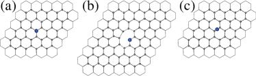
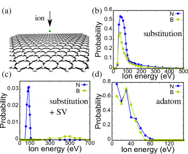
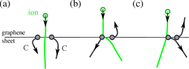
We started our simulations by calculating the probabilities for an irradiation event to produce the most typical defect structures (some of which are shown in Fig. 1), as functions of ion energy for both B and N ions. The most prolific outcomes were substitution (exactly one C replaced by the B/N), substitution with a neighboring vacancy, single vacancy (SV) and double vacancy (DV). At low energies, we also frequently observed the dopant atom attached to the perfect graphene structure as an adatom. A schematic of the simulation setup as well as the defect creation probabilities of these structures are presented in Fig. 2 for those defects involving the dopant atom (presented in Fig. 1), in Fig. 3 for SV and in Fig. 4 for DV.
III.1 Incorporation of the dopant atom into graphene
The highest observed probability (55%) for any of the structures (except for adatom deposition at very low energies which naturally gives a probability of 100%) was seen for N substitution (Fig. 1b) at energies close to 50 eV (Fig. 2b). For substitution, it is intuitively clear that the probability should display a single peak at these energies: although the displacement threshold for a carbon atom is about 20 eV in a head-on collision, on average the ion must have a somewhat higher energy in order to displace the atom, as a nearly head-on collision is unlikely. For B substitution the maximum is slightly below 40% (Fig. 2b), and it appears at a slightly lower energy than for N. The lower energy for B ion is a results of the difference between the momentum transfer from B/N ions to the target atom while the lower probability arises from the smaller displacement cross section for the B ion. By comparing to noble gas ion irradiation results for single vacancy production in graphene Lehtinen2010 (substitution occurs when the ion is stopped after a successful sputtering of one target atom), it is easy to see that these features are indeed caused by the mass difference between the ions rather than chemical effects. For energies higher than 0.5 keV, very few ions were incorporated into the graphene atomic network. Instead, at high energies (where chemical effects are not important, as shown below) relatively larger vacancy-type defects will be produced Lehtinen2010 .
For nanotubes Kotakoski2005 ; Kotakoski2005a , the highest observed probability for B and N substitutions were similar to those found for graphene, although the exact values were slightly lower/higher for N/B. For both ions, the peaks in graphene appear at lower energies and are significantly narrower. This can be understood based on the geometrical differences between nanotubes and graphene. As a crude approximation, one can think of the nanotube as a parallelepiped with two walls perpendicular to the ion beam direction and two walls parallel to it. Therefore, it is possible for the ion to be slowed down by the first wall before the displacement takes place. This naturally leads to substitution events also at energies higher than what is observed for graphene, a two-dimensional system. What is perhaps more surprising is that the probabilities themselves are not much different. A priori one could have expected the nanotube structure to yield roughly twice the number of substitutions due to the two walls parallel to the beam. However, since it also takes energy to penetrate the first wall, this is manifested only at energies above those for the peaks observed in graphene.
Another type of observed substitutions is a result of an irradiation event in which the ion has first displaced two carbon atoms from graphene and then remains in the place of one of the displaced atoms in a pyridine-like configuration Ewels05rev , as shown in Fig.1(b). We never observed pyrrolene-like structures Ewels05rev in which the nitrogen/boron atom occupies a site in a five-membered atomic ring. This situation may be more probable in nanotubes Lin2009 where such configurations are assisted by the curvature. Since it was not seen in the nanotube ion irradiation simulations Kotakoski2005 ; Kotakoski2005a either, it may also be a feature which only occurs when nitrogen dopants are introduced during synthesis.
Since two atoms must be displaced for a dopant-vacancy–complex to be created, it correspondingly occurs at higher energies than the perfect substitution. The probability for this process is presented in Fig. 2c as a function of the ion energy. Surprisingly, the probabilities are significantly different for B and N ions, with a probability for N being larger by more than two orders of magnitude. However, even in this case the probability maximum is only %. Again, the difference is mostly due to the mass difference between the B and N ions. For the heavier N, with increasing energies the scattering process leads to displacements of the carbon atoms in the directions perpendicular to the initial ion direction, as described in Ref. Lehtinen2010 , while the ion only slightly deviates from the original direction. Hence, the defect is produced by simultaneous displacement of two carbon atoms while the ion itself stops at the graphene sheet. However, for B, which is lighter than C, the situation is opposite; with higher energies the ion itself is scattered in a direction parallel to the plane where it will be scattered again by another C atom and thus eventually leaves the structure.
The probability for creating the dopant-vacancy–complex in nanotubes Kotakoski2005 ; Kotakoski2005a was similar to graphene values for N but significantly higher for B (at optimal energies). This is due to the fact that the projected atomic density in the direction parallel to the initial ion trajectory is in some areas much higher for nanotubes than for graphene due to curvature. Therefore, even though the displacement cross section for the B ion with respect to target atoms is relatively small at energies required to displace two atoms, simultaneous displacement of an atom pair is still more likely than in the case of graphene.
As mentioned above, we checked all observed final structures with DFT calculations to ensure their stability beyond the description provided by the bond-order potential. Indeed, both of the substitution cases remained stable during the structure optimization (the DFT-optimized structures are shown in Fig. 1). The formation energy for the perfect substitution is ca. eV lower than that for the pyridine-like two-coordinated configuration. Therefore, one can expect that in the case of migrating carbon adatoms on the graphene surface, the pyridine-like configurations tend to get filled with carbon atoms to form a structure similar to perfect substitution. As has been shown previously Kotakoski2005a , the formation energies of the substitutional impurities in graphene are a few electron-volts with a somewhat higher formation energy for boron substitution.
III.2 Creation of single vacancies
In addition to substitutional impurities, ion-implantation should inevitably result in the formation of various irradiation-induced defects in graphene Banhart2010 ; Krasheninnikov2010 . Among these, single vacancies have the highest probability to appear. In the case of N irradiation, it reaches its maximum at ca. 125 eV with a value of 55% (Fig. 3a). This very narrow peak overlaps with a broad peak with its maximum (35%) at ca. 400 eV. Surprisingly, for B, only a slight effect of the first peak is seen as a shoulder of the second peak. In this case the peak has a maximum of 35% at 180 eV (Fig. 3a). The narrower low-energy peak results from a chemical interaction between the ion and one of the target carbon atoms. From a case-by-case analysis of the distance between the ion and the sputtered atom as a function of time, it is clear that the attractive interaction between the projectile and recoil atom is responsible for the production of single vacancies at energies within this peak via a mechanism where the ion pulls one carbon atom with itself while penetrating the sheet, as sketched in Fig. 3b. This effectively results in the formation of a dimer, which may eventually be broken, as also sketched in Fig. 3b.
In Fig. 3c,d we show the effect of the attraction by subtracting those cases where the ion and a carbon atom form a dimer during the sputtering process from the overall probability for the single vacancy creation. For B, this process completely accounts for the shoulder of the single vacancy probability peak. However, for N, it only accounts for the lower energy end of the narrow peak. This effect can also be directly explained by comparing the masses of the ions, and taking into account that both N and B have an attractive interaction with carbon atoms. Because B is lighter than C, it is unlikely that it will escape the carbon atom after successfully displacing it at the energy range where the attraction plays a role. Thus, the dimer remains stable after the sputtering event. However, for the heavier N, the ion can effectively pull one carbon atom after itself but still retain enough kinetic energy to escape the atom thus breaking the dimer. By carefully comparing cases with exactly the same impact parameters, except for a slight change in kinetic energy of the ion, in which the lower energy produced a single vacancy and the higher energy did not, we concluded that this swift chemical sputtering process (in principle similar to what has been observed in Ref. Salonen2001 for hydrogen ions) indeed completely explains the observed narrow peak in the single vacancy production probabilities for both N and B ions.
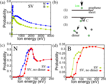
These results are in line with Ar irradiation simulations carried out for nanotubes Tolvanen2007 , as well as with the noble gas irradiation studies for graphene Lehtinen2010 . If one ignores the chemical sputtering which does not occur for the noble gases, the single vacancy probabilities for B/N appear at energies between those for He and Ne in the order of increasing mass, as one would expect. Also the functional form is similar to that observed for He and Ne irradiation, even reproducing the broadening of the probability peak with increasing mass of the projectile Lehtinen2010 . Therefore, also this comparison shows that the additional narrow peak must be caused by a chemical effect.
III.3 Creation of double vacancies
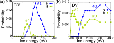
The last of the often observed defects is DV. The highest probability (16%) for this defect was found upon N irradiation at energies close to 110 eV (Fig. 4a). For B, the corresponding peak maximum occurred at 70 eV with a value of 6% (Fig. 4b). In addition to this first peak, the probability for B irradiation contains two other, much broader, peaks. The first of these (#2) occurs with a probability of less than 1% at energies between 0.14 keV and 1.4 keV. The second one (#3) appears with a similar probability maximum at energies closer to 2 keV. This peak extends to energies higher than those included in this study. For N, only the second one of these high energy peaks (#3) appears. From the three peaks, each of which occur at the characteristic energy range, it’s easy to predict that there are three mechanisms for the double vacancy production. These three mechanisms are illustrated in Fig. 5.
The lowest energy peak is due to a direct impact by the ion with two carbon atoms when the ion strikes in the middle of the bond between these atoms (Fig. 5a). For energies exceeding the value corresponding to the maximum in the curve, the scattering cross section for the ion and a target atom becomes so small that it is impossible for the ion to displace two atoms simultaneously. For the heavier N ion, the correspondingly larger cross section extends the probability peak over the energy range observed for B. Due to the larger displacement cross section also the peak maximum appears with a higher value for N. This also explains the difference observed for the ions in the case of vacancy-dopant–complexes, which are directly linked to double vacancies.
The second mechanism (Fig. 5b), which does not occur for N, arises from the mass difference between the B ion and carbon atoms. Because B is lighter than C, at the intermediate energies it gets scattered in the in-plane direction so that it has enough kinetic energy left to sputter a second carbon atom. In the case of boron, this mechanism leads to the highest probability for the vacancy-dopant–complex defect in the case where the ion has enough energy to displace both carbon atoms but becomes trapped in the carbon network. For the heavier N, this never occurs since it is rather the carbon atom which gets scattered in the in-plane direction. Similar behavior is also evident in the noble gas irradiation results Lehtinen2010 where two peaks are observed for the Ne ion irradiation (Ne mass is about 1.4 times larger than that of N), similar to the N irradiation in the present study.
The third of the observed double vacancy creation mechanism (Fig. 5c) involves the displacement of one carbon atom in the in-plane direction by the ion, which then causes the sputtering of a second atom. In the case of noble gas ions heavier than Ne, the two peaks (corresponding to peaks one and three for B irradiation) overlap so that the separation of the peaks becomes impossible Lehtinen2010 .
III.4 Dopant as an adatom
Obviously, for ion energies below the threshold for creating a single vacancy, the dopant will be attached to the pristine graphene structure as an adatom (if it does not go through the middle of the hexagon). Depending on the impact point and the energy of the projectile, it is also possible that the ion gets bounced back from the graphene sheet, which leads to a non-monotonous probability curve as a function of the ion energy (Fig. 2d). Although it is rather unlikely that the adatom configuration would spontaneously transform to a substitutional defect, it is possible that the adatoms will take the position of a missing atom in a single or double vacancy created during the irradiation, since the migration barriers for B/N adatoms are in the range of 0.1–1.1 eV on graphenic surfaces Lehtinen2003 ; Kotakoski2005a .
From a simple formation energy consideration at the thermodynamical equilibrium, it would also be beneficial for nitrogen dimers to break in order to fill in single vacancies in graphene (according to DFT calculations, this would lead to a significant energy gain of more than 6 eV per nitrogen atom). This could occur during annealing in a N2 atmosphere. However, this process would require the breakage of the N dimer which is among the strongest molecules in nature. Recent experiments indeed showed Guo2010 that annealing in a N2 atmosphere does not lead to N-doping of defective graphene. However, using a molecular environment in which the nitrogen (or boron) atoms are less strongly bound, such as NH3, will provide dopant atoms to fill the vacancies, as was demonstrated in Ref. Guo2010 .
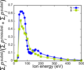
III.5 Relative probability for substitution
Naturally, one of the critical factors in using ion irradiation to dope a nano-object such as graphene, with plenty of free space for the target atoms to escape, is the amount of other defects created during the implantation. Luckily, the production of single vacancies, and especially more complex defects, occurs mainly at energies higher than that of the highest substitution probability. The total probability for creating any other defect during nitrogen ion irradiation at 40 eV is 29%. For boron, the corresponding value at 100 eV is 27%. These energies correspond to 10% substitution probabilities at the lower and higher end for nitrogen and boron, respectively. At the most efficient doping energy (50 eV) for N, the probability for creating any other defects is 32%. For B at this energy, in 36% of the events are other defects created. These relative probabilities, defined as the ratio of sum of probabilities for the different substitution cases () to the sum of probabilities for all defects (), for B/N substitution are shown in Fig. 6 as a function of the irradiation energy. An obvious way to overcome any problems arising from creating a substantial amount of single vacancies during the substitution is to combine irradiation with two energies; one at the substitution maximum and another one below the single vacancy creation threshold. This would allow deposition of dopant adatoms which could fill in the created vacancies. Although we are unaware of any experiments where such a method would have been used, this is in many ways similar to that of annealing in a suitable molecular atmosphere providing the dopant atoms, as presented in Ref. Guo2010 .
IV Conclusions
As we have shown above, ion irradiation can be used for implanting B/N ions into graphene. The most efficient doping energies are, according to our simulations, close to 50 eV for both ions. The high-probability peaks are wide enough to allow doping also at various energies both below and above the maximum. For example, substitution probability for nitrogen ion remains over 10% for energies between 40 eV and 105 eV, and for boron between 40 eV and 100 eV. Assuming a control over ion energies and the possibility to use focused ion beams, one can envisage fabrication of spatially-non-uniform graphene based materials where N and B doped areas can be made with a resolution of better than 5 nm. As the defect structures which we observed during our MD simulations were confirmed to be at least metastable by our DFT calculations, and because our earlier theoretical predictions Kotakoski2005 ; Kotakoski2005a on ion implantation into carbon nanotubes have been experimentally corroborated Morant2006 , one can expect that our results for graphene give a good indication of the outcome of actual experiments.
As a conclusion, our computational work combining classical MD simulations and DFT total energy calculations indicate, similar to what has been shown for carbon nanotubes, that ion irradiation is a promising method for creating hybrid C-B/N structures for future applications in the realm of nanoelectronics. The beneficial irradiation energy proved out to be 50 eV with substitution probabilities of 50% for N and 40% for B. At these energies the probability for creating other defects is close to 30–50%. By lowering the implantation energy below the threshold for creating single vacancies or by annealing in a suitable molecular environment (such as NH3), the vacancies created while doping can be eliminated via dopant atoms to reach a significantly higher substitution/defect ratio. We also reported a surprisingly effective chemical sputtering method for N irradiation at low energies (125 eV) which leads to production of single vacancies.
Acknowledgments
We thank the Finnish IT Center for Science for generous grants of computer time, and Academy of Finland for funding through several projects.
References
- (1) K. S. Novoselov, A. K. Geim, S. V. Morozov, D. Jiang, Y. Zhang, S. V. Dubonos, I. V. Grigorieva, and A. A. Firsov, Science 306, 666 (2004).
- (2) S. Iijima, Nature 354, 56 (1991).
- (3) A. H. Castro Neto, F. Guinea, N. M. R. Peres, K. S. Novoselov, and A. K. Geim, Rev. Mod. Phys. 81, 109 (2009).
- (4) D. J. Appelhans, Z. Lin, and M. T. Lusk, Phys. Rev. B 82, 073410 (2010).
- (5) X. Li et al., Science 324, 1312 (2009).
- (6) S. Bae et al., Nature Nanotech. 5, 574 (2010).
- (7) Q. Yan et al., Nano Lett. 7, 1469–1473 (2007).
- (8) B. Huang et al., Appl. Phys. Lett. 91, 253122 (2007).
- (9) A. L. M. Reddy, A. Srivastava, S. R. Gowda, H. Gullapalli, M. Dubey, and P. M. Ajayan, ACS Nano 4, 6337 (2010).
- (10) X. Wang, X. Li, L. Zhang, Y. Yoon, P. K. Weber, H. Wang, J. Guo, and H. Dai, Science 324, 768 (2009).
- (11) D. Wei, Y. Liu, Y. Wang, H. Zhang, L. Huang, and G. Yu, Nano Letters 9, 1752 (2009).
- (12) D. J. Late, A. Ghosh, K. Subrahmanyam, L. Panchakarla, S. Krupanidhi, and C. Rao, Solid State Communications 150, 734 (2010).
- (13) H. Zheng and W. Duley, Phys. Rev. B 78, 155118 (2008).
- (14) A. Lherbier, X. Blase, Y.-M. Niquet, F. Triozon, and S. Roche, Phys. Rev. Lett. 101, 036808 (2008).
- (15) N. M. R. Peres, F. D. Klironomos, S.-W. Tsai, J. R. Santos, J. M. B. L. dos Santos, and A. H. Castro Neto, EPL (Europhysics Letters) 80, 67007 (2007).
- (16) B. Zheng, P. Hermet, and L. Henrard, ACS Nano 4, 4165 (2010).
- (17) S.-S. Yu and W.-T. Zheng, Nanoscale 2, 1069 (2010).
- (18) Z. Wang, H. Hu, and H. Zeng, Appl. Phys. Lett. 96, 243110 (2010).
- (19) X. H. Zheng, I. Rungger, Z. Zeng, and S. Sanvito, Phys. Rev. B 80, 235426 (2009).
- (20) R. Peköz and Şakir Erkoç, Physica E: Low-dimensional Systems and Nanostructures 42, 110 (2009).
- (21) B. Biel, X. Blase, F. Triozon, and S. Roche, Phys. Rev. Lett. 102, 096803 (2009).
- (22) S. S. Yu, W. T. Zheng, and Q. Jiang, IEEE Transactions on Nanotechnology 9, 243 (2010).
- (23) S. S. Yu, W. T. Zheng, and Q. Jiang, IEEE Transactions on Nanotechnology 9, 78 (2010).
- (24) J. Huang, L. Qi, and J. Li, Nano Research 3, 43 (2010).
- (25) J. Ozaki, N. Kimura, T. Anahara, and A. Oya, Carbon 45, 1847 (2007).
- (26) H. Lin, R. Arenal, S. Enouz-Vedrenne, O. Stephan, and A. Loiseau, J. Phys. Chem. C 113, 9509 (2009).
- (27) L. Ci et al., Nat Mater 9, 430 (2010).
- (28) K. Raidongia, A. Nag, K. P. S. S. Hembram, U. V. Waghmare, R. Datta, and C. N. R. Rao, Chem. Eur. J. 16, 149 (2010).
- (29) R. B. Pontes, A. Fazzio, and G. M. Dalpian, Phys. Rev. B 79, 033412 (2009).
- (30) O. Lehtinen, J. Kotakoski, A. V. Krasheninnikov, A. Tolvanen, K. Nordlund, and J. Keinonen, Phys. Rev. B 81, 153401 (2010).
- (31) B. Guo, Q. Liu, E. Chen, H. Zhu, L. Fang, and J. R. Gong, Nano Letters (2010), doi: 10.1021/nl103079j.
- (32) J. Kotakoski, J. A. V. Pomoell, A. V. Krasheninnikov, and K. Nordlund, Nucl. Instr. and Meth. in Phys. Res. B 228, 31 (2005).
- (33) J. Kotakoski, A. V. Krasheninnikov, Y. Ma, A. S. Foster, K. Nordlund, and R. M. Nieminen, Phys. Rev. B 71, 205408 (2005).
- (34) A. Tolvanen, J. Kotakoski, A. V. Krasheninnikov, and K. Nordlund, Appl. Phys. Lett. 91, 173109 (2007).
- (35) A. V. Krasheninnikov and K. Nordlund, Phys. Rev. B 71, 245408 (2005).
- (36) K. Matsunaga, C. Fisher, and H. Matsubara, Jpn. J. Appl. Phys. 39, 48 (1999).
- (37) D. W. Brenner, Phys. Rev. B 42, 9458 (1990).
- (38) H. J. C. Berendsen, J. P. M. Postma, W. F. van Gunsteren, A. DiNola, and J. R. Haak, J. Chem. Phys. 81, 3684 (1984).
- (39) J. Tersoff, Phys. Rev. Lett. 56, 632 (1986).
- (40) J. Kotakoski, C. H. Jin, O. Lehtinen, K. Suenaga, and A. V. Krasheninnikov, Phys. Rev. B 82, 113404 (2010).
- (41) C. Morant, J. Andrey, P. Prieto, D. Mendiola, J. M. Sanz, and E. Elizalde, Phys. Stat. Sol. 203, 1069 (2006).
- (42) A. V. Krasheninnikov and K. Nordlund, J. Appl. Phys. 107, 071301 (2010).
- (43) G. Kresse and J. Furthmüller, Comput. Mat. Sci. 6, 15 (1996).
- (44) G. Kresse and J. Furthmüller, Phys. Rev. B 54, 11169 (1996).
- (45) P. E. Blöchl, Phys. Rev. B 50, 17953 (1994).
- (46) J. P. Perdew, K. Burke, and M. Ernzerhof, Phys. Rev. Lett. 77, 3865 (1996).
- (47) H. J. Monkhorst and J. D. Pack, Phys. Rev. B 13, 5188 (1976).
- (48) C. P. Ewels and M. Glerup, J. Nanosci. Nanotech. 5, 1345 (2005).
- (49) F. Banhart, J. Kotakoski, and A. V. Krasheninnikov, ACS Nano 5, 26–41 (2010).
- (50) E. Salonen, K. Nordlund, J. Keinonen and C. H. Wu, Phys. Rev. B 63, 195415 (2001).
- (51) P. O. Lehtinen, A. S. Foster, A. Ayuela, A. V. Krasheninnikov, K. Nordlund, and R. M. Nieminen, Phys. Rev. Lett. 91, 017202 (2003).