Transition Edge Sensor Thermometry for On-chip Materials Characterization
Abstract
The next generation of ultra-low-noise cryogenic detectors for space science applications require continued exploration of materials characteristics at low temperatures. The low noise and good energy sensitivity of current Transition Edge Sensors (TESs) permits measurements of thermal parameters of mesoscopic systems with unprecedented precision. We describe a radiometric technique for differential measurements of materials characteristics at low temperatures (below about ). The technique relies on the very broadband thermal radiation that couples between impedance-matched resistors that terminate a Nb superconducting microstrip and the power exchanged is measured using a TES. The capability of the TES to deliver fast, time-resolved thermometry further expands the parameter space: for example to investigate time-dependent heat capacity. Thermal properties of isolated structures can be measured in geometries that eliminate the need for complicating additional components such as the electrical wires of the thermometer itself. Differential measurements allow easy monitoring of temperature drifts in the cryogenic environment. The technique is rapid to use and easily calibrated. Preliminary results will be discussed.
I Introduction
The problem of characterizing the thermal properties of mesoscopic thin-film structures at low temperatures (below ), in particular their thermal conductances and heat capacities as a function of temperature, remains one of the key challenges for designers of ultra-low-noise detectors. This problem is not confined exclusively to the detector community.[1] These measurements require small, easily fabricated, easily characterized thermometers. Techniques are already used such as Johnson noise thermometry (JNT) using thin film resistors as noise sources with dc-SQUID readout or measurements of thermal properties using Transition Edge Sensors (TESs) but both have practical limitations. JNT can perform measurements over a reasonable temperature range and is in principal a primary thermometer but is in practice secondary because of stray resistance in the input circuit to the SQUID that must be calibrated. The achievable measurement precision,, for a source at temperature is given by the radiometer equation
| (1) |
where is the measurement time and is the measurement bandwidth.[2, 3] In practice the bandwidth is limited by the source resistance and the input inductance of the SQUID to a few 10’s of kHz. This gives for with . This is the precision that we found in practice.[4] TESs can be used to determine conductances by measuring the power dissipated in the active region of the device where electrothermal feedback (ETF) stabilizes the TES at its transition temperature, , as a function of the temperature of the heat bath, . These measurements are widely reported particularly in the context of measurements of the thermal conductance of silicon nitride films, but a key limitation is that the technique measures thermal properties averaged over a large temperature difference (i.e. between and ) and the films under study must support additional (generally superconducting) metalization to provide electrical connection. A problem arises if the thermal properties are themselves a function of temperature. A technique for measuring conductances or heat capacities of micron-scale objects rapidly over a reasonable temperature range without additional overlying films certainly seems to be required. The proposed technique permits true differential measurements of conductance (i.e with small temperature gradients), in a geometry without complicating additional metalization. Measurements of heat capacities are also possible. The technique is easy to implement, simple to calibrate and rapid to use.
We recently demonstrated highly efficient coupling of very broadband thermal power between the impedance-matched termination resistors of a superconducting microstrip transmission line.[5] The efficiency of a short microstrip ( was better than 97% for source temperatures up to . When the coupling efficiency is very high the power transferred along a superconducting microstrip between a source and a TES can be used as a fast, accurate thermometer. [6] The practical temperature sensitivity is determined by the TES low-frequency Noise Equivalent Power, . The limiting temperature sensitivity is determined by the very-wide radio-frequency bandwidth of the microstrip coupling so that we substitute in Eq. 1 and is the equivalent rf-bandwidth of a blackbody source at temperature .
II TES thermometry
We begin by reviewing the technique of TES thermometry for a simple geometry. In section II-B we describe the full thermal circuit used in the measurements of conductances. In sections II-C and II-D we describe how the conductances are determined experimentally.
II-A A simple geometry
A thermal circuit for a simple geometry for TES thermometry is shown in Fig. 1. A source of total heat capacity which could be a thermally isolated silicon nitride () island is connected to a TES also formed on a island by a conductance formed from a resistively-terminated superconducting microstrip. Broadband power is transferred between the impedance-matched termination resistors of the microstrip which has thermal conductance . Over a portion of its length the microstrip crosses the Si substrate so that any phonon conductance is efficiently heat sunk to the bath. arises from conduction due to photons. The source and TES are connected to a heat bath at temperature by conductances and respectively which include the contribution from the phonon conductance of dielectric of the microstrip. Heaters permit the source temperature to be varied and the TES to be calibrated.

Changes in the power coupling along the microstrip are measured using the TES which is in close proximity to its termination resistor. For low source temperatures , all of the power is contained within the pair-breaking threshold of the superconducting Nb, where is Planck’s constant and is the superconducting energy gap. The power transmitted between the source at temperature and the TES at its transition temperature is given by
| (2) |
where is the frequency, and is the Bose-Einstein distribution, and we have assumed that the coupling is loss-less. If the source temperature is low all of the power is contained well-within the cut-off frequency of the microstrip and the upper limit of may be set to infinity. Eq. 2 then has the solution
| (3) |
The measurement conductance is . determines how changes in source temperature affect power flow to the TES.
To calibrate the thermometry we need to know the low-frequency TES current-to-power responsivity, . This is measured by applying slowly-varying power, , to the known heater resistance on the TES island and measuring the change in detected current . The responsivity is then . As the source temperature is changed using the source heater, the power incident on the TES changes as given by Eq. 3. Measuring the change in the current flowing through the TES, , determines the change in detected power . Noting that , and since ETF fixed the TES’s temperature at , we can determine the source temperature to a good approximation as
| (4) |
The practical temperature measurement precision is determined by the low-frequency TES so that[6]
| (5) |
Here we have intentionally omitted thermal fluctuations of the source island which we consider a signal in this geometry. For the achievable temperature precision is for and . This is two orders of magnitude better than JNT.
II-B The measured geometry
In the full geometry two source islands , are connected by the subject under test here a conductance, . The subject may be more complicated. Each source island is connected to its own TES by a microstrip. Figure 2 shows the full thermal circuit.

We measure the quiescent TES currents to monitor and subtract small drifts in the substrate temperature or the electronics. The measurement precision of the temperature of either source, , with a measurement time is determined by the low-frequency TES so that
| (6) |
and the temperature measurement precision for this differencing approach includes a contribution from the bath temperature measurement. We have also now explicitly included the effect of thermodynamic fluctuations in the temperatures of the sources of heat capacity since these fluctuations directly affect the precision with which the source temperature can be determined.
II-C Measurement of the conductance
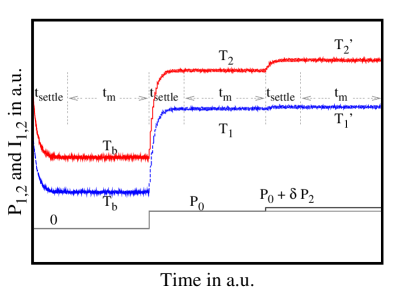
We measure the interconnect conductance in a three step process. A schematic of the measurement cycle is shown in Fig. 3. In the first step the quiescent TES currents are measured. Then dc power is input to both source islands raising the temperatures from the bath temperature to , . We find and we quantify the effect of later. Finally power to is stepped by an additional small amount raising the island temperatures to and . Since both and are small the measurement is differential. For the next temperature sample the process is repeated with incremented . The power steps are adjusted in software to give approximately constant increments and differences in temperature across the range of temperatures measured. One complete measurement cycle (i.e. ), with a short settling time between each measurement step to accommodate thermal response times, defines a ‘frame’ time. The frame must be measured in a time less than the Allan time of the system.
The power flow across a conductance connecting thermal reservoirs at temperatures , can be written for notational convenience as
| (7) |
where the over-set line denotes averaging. If is small then the power flow can be linearized so that . Ignoring for now the small conductance of the microstrips, the input powers and resultant temperatures are related by
| (8a) | ||||
| (8b) | ||||
| (8c) | ||||
| (8d) | ||||
Subtracting 8a from 8c, 8b from 8d and using, for example,
| (9) |
where and the final equality follows since is small, we find
| (10) |
and . Finally the effect of conductance along the microstrip needs to be included. The result is
| (11) |
II-D Measurement of the conductances ,
The conductance to the bath at a given temperature is measured in a two-step procedure where we measure the quiescent TES current () and the effect of applying equal power to both islands and measuring the changes in and . The next temperature sample uses incremented . This measurement is rapid. With , 500 data points are acquired in less than 15 minutes. In the analysis we use Eqs. 8a and 8b and assume . This introduces an inevitable error in the analysis and the magnitude is of order . Experimentally the error is small . A fifth-order polynomial is fitted to the data and the conductances , found by differentiation. Note that since the temperature difference may be large this measurement is temperature-averaged.
III Measured device
An optical image of the device described here is shown in Fig. 4.
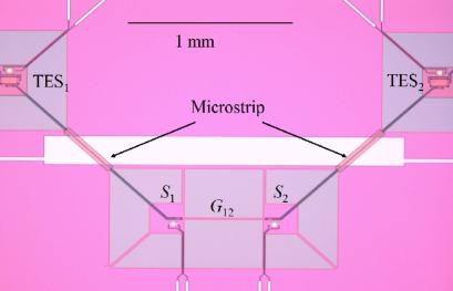
The measured conductance labelled is a long thin bar of dimensions formed by reactive ion and deep reactive ion etching of a nitride-coated Si wafer. carries no additional films. connects two larger -thick nitride source islands and themselves isolated from the Si wafer by four supporting nitride legs, two of length two of length each of width . One of the longer legs also carries a Nb microstrip line. The microstrip is terminated by an impedance-matched AuCu termination resistor at each end. Each island also supports a square AuCu resistor with Nb bias lines that can be used as a heater to modulate the temperature of the sources. The microstrips run over the Si wafer then onto nitride islands which support TESs. Routing of the microstrips in this way ensures that the phonon conductance associated with the microstrip dielectric is efficiently heat-sunk to the bath. The TES islands also include AuCu resistors with Nb bias lines that allow the power-to-current responsivity of the TESs to be measured.
AuCu resistors are thick, Nb bias lines and the ground plane of the microstrip are thick. The microstrip dielectric is sputtered and is thick. The TESs use our standard higher temperature MoCu bilayer layup with and of Mo and Cu respectively. The fabrication route is identical with our usual process for MoCu TESs.[7] The TESs are voltage biased and read-out with SQUIDs. The device is measured in a He-3 refrigerator with a base temperature of 259 mK. The transition temperature of the TESs described here was which is slightly higher than reported in our earlier work with the same Mo-Cu bilayer lay-up. As a result the conductance to the bath of the TESs is increased and the measured TES Noise Equivalent Power is .
IV Results and Discussion
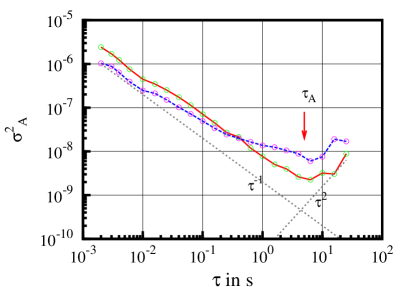
The Allan variance statistic, where is the integration time, provides an exceptionally powerful diagnostic of system stability and a plot of the variance as a function of identifies the optimum time for signal averaging.[8, 9] In the Allan plot, a log-log plot of as a function of , underlying fluctuations with frequency-domain power spectra varying as show a dependence. Hence white noise with has a characteristic. noise shows no dependence on integration time and drift exhibits a dependence with . Figure 5 shows measured Allan variances for both SQUID systems with biased TESs and the bath temperature at . The measured characteristic indicates that white noise is reduced by time-integration up to a maximum of order . The dashed lines show the expected behaviour for white noise with a slope and for drift with a slope of . This shows that drift limits these measurements. Guided by the Allan plot, we chose a sample time being data points sampled at and . For the conductance measurements with three power steps the total frame time is 2.8 s at each sample temperature.
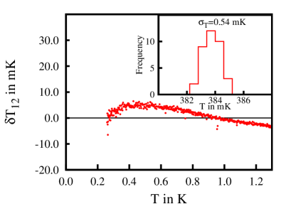
Applying equal power to both sources, and were determined. As discussed earlier the analysis introduces an unavoidable error in the measurement of and depending on . Figure 6 shows the difference in temperature for equal powers applied to both islands as a function of average island temperature. The difference is small and a maximum of about at 500 mK. Since is small we will see that the error is negligible. The temperature difference implies a difference in conductance for the two notionally identical conductances , of about between 0.26 and 1.3 K. The temperature dependence of evident in Fig. 6 is also unexpected. It does not seem that the difference can be accounted for by experimental uncertainty (such as in the calibration of the TES responsivities). One possibility might be differences in the actual coupling efficiencies of the microstrip lines.
The inset of Fig. 6 shows a histogram of calculated temperatures for repeated measurements of a source temperature near . The measured precision compares well with the value calculated from Eq. 6 which gives for the measurement time used and the measured .
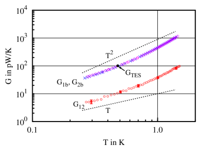
Figure 7 shows measured conductances , and as a function of temperature. Representative error bars for determined from the variance of repeated measurements are indicated. We can now estimate the magnitude of the error in and . The maximum temperature difference occurs near where is greatest. We find , but less than this over most of the temperature range. This is considered acceptable. We also show the variation with temperature if with a constant. The dotted lines show dependencies and 2. There is a strong suggestion here that a simple power law does not account for the conductance across this measurement range. At the highest temperatures , at the lowest . A reduction of the exponent may be expected at low temperatures if dominant phonon wavelengths start to become comparable to the nitride thickness. The single dot in Fig. 7 is the measured for one of the TESs obtained in the standard way by measuring the power plateau in the ETF region of the current-voltage characteristic as a function of the bath temperature. This single point represents approximately 2 hours of data taking. By contrast the conductances to the bath , plotted in Fig. 7 are found from 500 measurements of temperature acquired in 15 minutes. A comparable acquistion time measures with 50 data points with additional signal averaging.
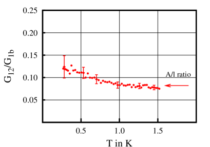
Figure 8 shows the ratio of to as a function of temperature. The simplest model for power flow along, or the conductance of, a uniform bar would assume that the power scales as the ratio of cross-sectional area, , to length, . From the dimensions of the nitride support legs for the source islands and the dimensions of we calculate a conductance ratio of 0.082. This ratio includes the conductance associated with the dielectric of the microstrip lines and the smaller contribution from the Nb wiring all of which we assume are equal to that of . The variation of the ratio is experimentally significant and may already illustrate the difference between thermal properties averaged over a temperature range and the true differential measurement.
V Conclusion
We have described our first true-differential measurements of thermal conductances of a micron-scaled object at low temperatures using microstrip-coupled TES thermometry. The temperature precision is already significantly greater than that achievable with JNT with the same measurement time. The measurements are rapid and easily calibrated. The achieved precision already strongly suggests that the thermal transport characteristics of the nitride structure are not described by a simple power-law across the temperature range to . The device under test can be fabricated without additional metalization for wiring. It should be straight-forward to include specific layers on the nitride test structure to measure particular thermal properties in a controlled manner. In the future we expect to be able to explore the temperature dependence of heat capacities of thin films such as including possibly measurements of time dependent heat capacity. We will explore the effect on conductance of superposed layers: for example, does thermal conductance in thin multilayers really scale as total thickness? We also see the possibility of exploring the engineering of the nitride to realise phononic structures, to achieve reductions of the conductance in compact nitride structures needed for the next generation of ultra-low-noise detectors.
Acknowledgment
We would like to thank Michael Crane for assistance with cleanroom processing, David Sawford for software and electrical engineering and Dennis Molloy for mechanical engineering.
References
- [1] F. Giazotto, T. T. Heikkilä, A. Luukanen, A. M. Savin, and J. P. Pekola, “Opportunities for mesoscopics in thermometry and refrigeration: Physics and applications,” Reviews of Modern Physics, vol. 78, no. 1, p. 217, 2006.
- [2] J. D. Kraus, Radio Astronomy, 2nd ed. New York: McGraw-Hill, 1986.
- [3] D. R. White, R. Galleano, A. Actis, H. Brixy, M. D. Groot, J. Dubbeldam, A. L. Reesink, F. Edler, H. Sakurai, R. L. Shepard, and J. C. Gallop, “The status of Johnson noise thermometry,” Metrologia, vol. 33, no. 4, pp. 325–335, 1996.
- [4] K. Rostem, D. Glowacka, D. J. Goldie, and S. Withington, “Technique for measuring the conductance of silicon-nitride membranes using Johnson noise thermometry,” J. Low Temp. Phys., vol. 151, pp. 76–81, 2008.
- [5] K. Rostem, D. J. Goldie, S. Withington, D. M. Glowacka, V. N. Tsaneva, and M. D. Audley, “On-chip characterization of low-noise microstrip-coupled transition-edge sensors,” J. Appl. Phys., vol. 105, p. 084509, 2009.
- [6] D. J. Goldie, K. Rostem, and S. Withington, “High resolution on-chip thermometry using a microstrip-coupled transition edge sensor.” Accepted for publication in J. Appl. Phys., 2010.
- [7] D. M. Glowacka, D. J. Goldie, S. Withington, M. Crane, V. Tsaneva, M. D. Audley, and A. Bunting, “A fabrication process for microstrip-coupled superconducting transition edge sensors giving highly reproducible device characteristics,” J. Low Temp. Phys., vol. 151, pp. 249–254, 2008.
- [8] D. W. Allan, “Statistics of atomic frequency standards,” Procs. IEEE, vol. 54, pp. 221–230, 1966.
- [9] R. Schieder and C. Kramer, “Optimization of heterodyne observations using Allan variance measurements,” ASTRONOMY & ASTROPHYSICS, vol. 373, pp. 746–756, 2001.