Multi-component Transparent Conducting Oxides: Progress in Materials Modelling
Abstract
Transparent conducting oxides (TCOs) play an essential role in modern optoelectronic devices through their combination of electrical conductivity and optical transparency. We review recent progress in our understanding of multi-component TCOs formed from solid-solutions of ZnO, In2O3, Ga2O3 and Al2O3, with a particular emphasis on the contributions of materials modelling, primarily based on Density Functional Theory. In particular, we highlight three major results from our work: (i) the fundamental principles governing the crystal structures of multi-component oxide structures including (In2O3)(ZnO)n, named IZO, and (In2O3)m(Ga2O3)l(ZnO)n, named IGZO; (ii) the relationship between elemental composition and optical and electrical behaviour, including valence band alignments; (iii) the high-performance of amorphous oxide semiconductors. From these advances, the challenge of the rational design of novel electroceramic materials is discussed.
pacs:
71.20.-b, 78.20.-e, 71.15.MbI Introduction
Transparent conducting oxides (TCOs) are defined by high electrical conductivity approaching that of a metallic compound, with the high transmission of photons in the visible range of the electromagnetic spectrum. The unique combination of these two features makes TCOs essential components of modern optoelectronic devicesthomas-907 ; edwards-2295 . The common electronic characteristic of -type TCO materials is a spatially delocalised, low energy, and low effective mass conduction band determined primarily by the metal orbitals. Such a state is achieved with oxides formed from closed-shell cations such as Zn(II), Ga(III) and In(III).
The prototype -type TCO is Sn-doped In2O3 (ITO), which has been the subject of intense study both experimentallyohya-240 ; wit-143 ; wit-142 ; weiher-2834 ; edwards-2295 ; hamberg-3240 ; king-116808 ; korber-165207 ; klein-1197 and theoreticallywalsh-167402 ; walsh-075211 ; walsh-10438 ; lany-045501 ; agoston-455801 ; tomita-051911 ; agoston-245501 ; medvedeva-125116 . Other examples of electron conducting TCOs include Al-doped ZnO, Ga-doped ZnO and F-doped SnO2. Typically these materials have electron carrier concentrations ranging from 1016 - 1021 cm-3, and electron mobility ranging from 10 to 1000 cm2V-1s-1, depending on the material quality and growth conditionsedwards-2295 .
In contrast to the delocalised conduction band wave-functions, the valence band states of hetero-polar metal oxides are typically localised O 2 states. Instead of resulting in mobile electron holes, acceptor doping of these materials results in deep localised states, which are stabilised by local lattice distortions - the formation of small polaronsschirmer-667 ; stoneham-255208 . To obtain hole conducting (-type) TCO materials, the principal approach has been to include a metal with filled low binding energy states at the top of the valence band, such as Cu(I), which can facilitate hole transportnie-066405 ; nie-075111 . Following the work of Hosono et al. on CuAlO2kawazoe-939 , many ternary Cu oxides have been explored for this purpose. The limitation of this class of material is the poor hole mobility ( 10 cm2V-1s-1) that arises from the relatively localised Cu bands, as well as the indirect electronic band gaps arising from the underlying lattice symmetry. Recent work has focused on other delafossite (CuO2, where is a trivalent cation) materials including CuGaO2nie-066405 , CuCrO2saadi-272 ; scanlon-035101 ; arnold-075102 , CuScO2huda-035205 and CuBO2scanlon-4568 , in addition to studies on related ternary copper oxides containing Sr and Pbkudo-220 ; nie-075111 ; godinho-2798 . Unfortunately for all Cu-based materials, the poor carrier mobility, which is directly related to the parent compound Cu2O, is difficult to overcome. In some cases, the existence of deep defect centersscanlon-096405 , which act as trapping centres for free carriers, pin the Fermi level well above the valence band, thus limiting the carrier densities achievable by doping.
The possibility of discovering alternative -type TCO compositions with superior material properties has led to the investigation of ternary and quaternary systems, with In2O3(ZnO)n (IZO) being one particular focus of attentionminami-971 ; taylor-90 ; hiramatsu-3033 ; kumar-073703 ; leenheer-115215 ; moriga-312 . These studies have highlighted the improved chemical and thermal stability of IZO compared to ITO, making it more desirable for commercial application. One issue with the utilisation of multi-component oxide materials is the difficulty in synthesising high-quality crystalline samples at low cost. To overcome this limitation, there has been an active interest in growing amorphous TCOs (a-TCOs)nomura-488 ; sun-1897 ; lee-843 ; taylor-3169 ; kumar-073703 . Amorphous oxides can exhibit electrical properties comparable to their crystalline phases, in contrast to traditional amorphous semiconductors. In amorphous systems, the underlying crystalline nature and translational symmetry of a material is lost; therefore, many atoms have unsaturated dangling bonds. For covalent materials such as Si, the dangling bond states are located at the center of the band gap, acting as both electron and hole traps, therefore, amorphisation of Si is associated with a substantial increase in electrical resistance, relative to the crystalline phasemott-1987 . For ionic or polar oxides, the dangling bond states are very close to the band edges; therefore, amorphisation of oxides usually does not create deep trap levels, which leads to the remarkable fact that a-TCOs can exhibit comparable transport properties relative to their crystalline counterparts, an effect that has only recently been understood through materials modellingwalsh-5119 ; robertson-1026 ; medvedeva-125116 ; hosono-2796 .
The physical and chemical properties of TCO materials have been the subject of many excellent reviews. In particular, the pioneering experimental work of Hosono et al. has been recently reviewedhosono-6000 , while a more comprehensive review of the field can be found in a themed issue of the Material Research Bulletinfortunato-242 . The chemistry of the ZnO-In2O3-SnO2 system was the focus of a detailed review by Hoel et al.hoel-3569 . From a theoretical perspective, comprehensive overviews focused on ZnO can be found in the works of Catlow et al.catlow-2234 , Lany and Zungerlany-235104 and Janotti and Van de Wallejanotti-165202 . In addition, Medvedeva and Hettiarachchi recently provided an in-depth analysis of the properties of complex TCOs based on trends in their physical propertiesmedvedeva-125116 .
In this Topical Review, we focus on recent advances in the theoretical understanding of multi-component TCOs. After briefly addressing the binary metal oxide components of the complex TCOs, we address a number of highlights from our recent investigations, including: (i) the fundamental principles governing the structures of multi-component crystalline and amorphous oxide systems; (ii) the relationship between composition and optoelectronic behaviour; (iii) the origin of high-performance for amorphous oxide semiconductors. From these advances, future directions in the field of transparent conducting semiconductors are discussed.
II Computational Methods
The workhorse technique in applied computational material science is Density Functional Theory (DFT)dft1 ; dft2 , for which Walter Kohn and John Pople shared the Nobel prize in 1998. In contrast to quantum chemical methods, which are concerned with the dimensional many-body wave-function, in DFT it is the electron density that is the key quantity to be optimised and from which all ground-state properties can be determined. The result is an ab initio method that can be applied to realistic material simulations in solid-state physics, organic chemistry, soft matter and related fields.
Approaches based on DFT are widely available in a number of academic and commercial packages, e.g. the codes VASPvasp1 , CASTEPcastep , Quantum-Espressoespresso and FHI-AIMSaims1 . The principal difference between all implementations is in the choice of the basis set, which is used to represent the single-particle Kohn-Sham wave-functions, plane-waves, augmented plane-waves with atomic orbitals, gaussian functions, Slater orbitals, numerical orbitals. The technical details of these approaches have been reviewed in detail elsewheremartin-2004 ; payne-1045 .
Evaluation of the total energy, within the DFT formalism, gives access to a range of thermodynamic properties including heats of formation, ionisation energies and phase stability. Furthermore, forces and stress can be calculated routinely, which provides the flexibility for a wide range of studies on structure determination, including, for example, global optimisationwoodley-937 ; walsh-8446 ; trimarchi-295212 ; hautier-3762 . The solution of the Kohn-Sham equations yield the eigenvectors and eigenvalues for the respective system, and hence, it can be used to understand the underlying bonding mechanics and electrical transport properties.
The limitations of DFT are concentrated in the exchange-correlation functional, which contains the description of all quantum mechanical effects for the system of interest. The exact form of the functional remains unknown and must be approximated, which is generally in the form of local or semi-local functionals, i.e. the local density approximationlda (LDA) or generalised gradient approximationpbe (GGA), respectively. Both approaches gives rise to an accurate description of the structural, electronic and thermodynamic parameters for most systems; however, they fail to give a proper description of particular properties and systems, in particular, highly correlated (strongly interacting) electronic statesperdew-5048 .
It has been well demonstrated that both the LDA and GGA exchange-correlation functionals underestimate the electronic band gaps of insulators and semiconductors due to a discontinuity in the wavefunction character at the band edgesperdew-1884 ; sham-1888 . For quantitative band gap predictions, the use of many-body approaches such as theoryhedin-796 are necessary; however, the use of non-local hybrid density functionals offers a means to reduce the error within the single-particle formalism. In the hybrid approach, a percentage of exact non-local Hartree-Fock exchange is added to a local or semi-local exchange-correlation functional. One caveat of this approach is that the amount of exact-exchange and spatial screening remains material and property dependentcora-2004 . One hybrid functional, which has had particular success in its application to oxides, is the Heyd-Scuseria-Ernzerhof (HSE06) formulationhse ; paier-154709 , in which 25% of exact exchange replaces the short-range GGA exchange potential.
III Binary Oxides
Here, we briefly discuss the bulk properties of the main binary components of the multi-ternary systems of interest, i.e. ZnO, In2O3, Ga2O3, and Al2O3. A number of the material properties are summarised in Table 1, including the band gaps, heat of formation, cation effective coordination numbers, and the partial charges resulting from Bader analysisbader ; bader-vasp of the equilibrium electron density. Absolute values of the partial charges derived from delocalised electron densities are not unique, and are generally smaller than the formal ionic chargejansen-10026 ; catlow-4321 , but relative changes in these values can still be instructive.
III.1 ZnO
ZnO is a material that has a rich solid-state physics and chemistry, with a range of applications that exploit its electronic, optical and piezoelectric propertiesozgur-041301 . Recently, magnetic doping of ZnO has been the subject of intense study, e.g. Co doped ZnO, where the ferromagnetic coupling between Co states can be electron mediated kittilstved-291 ; walsh-256401 ; walsh-159702 . In its ground-state, ZnO adopts the hexagonal wurtzite (wz) crystal structure (space group ) with lattice constants of Å and Å,ozgur-041301 in which the Zn and O ions form roughly tetrahedral coordinated environments. The experimental electronic band gap of ZnO is 3.44 eVmadelung-04 , which is direct in nature. As mentioned in the Introduction, the material properties of ZnO have been subject of recent review both from an experimentalozgur-041301 and computational perspectivecatlow-2234 ; janotti-165202 ; lany-235104 ; catlow-1923 ; sokol-267 .
III.2 In2O3
The high -type conductivity of In2O3 is exploited in many TCO device applications, which has greatly contributed to the rising cost of In metalhamberg-r123 . Indium oxide adopts the body-centred cubic (bcc) bixbyite lattice (space group ) with Åmarezio-723 , which is a defective superstructure of the fluorite mineral structure. The In cations form roughly octahedral structures, which implies an effective coordination number close to 6. As mentioned above, In2O3 is widely used as a TCO; however, the long-standing band gap problem of In2O3 was only recently resolved from a joint experimental and theoretical effortwalsh-167402 . The direct electronic band gap of the bulk material is of the order of 2.9 eVwalsh-167402 , and the large disparity between the electronic and optical band gaps ( eV) arises from a combination of dipole forbidden optical transitions and conduction band occupationwalsh-167402 ; walsh-075211 ; korber-165207 ; fuchs-155107 .
III.3 Ga2O3
Ga2O3 is a wide band gap metal oxide ( eV), which is used in lasers, as well as a dielectric coating in electrical devicespasslack-686 . Of the five crystal polymorphs, the stable phase (space group ) consists of close packed oxide ions, with Ga occupying a combination of the tetrahedral and octahedral holes (see the coordination numbers in Table 1). The equilibrium lattice parameters are Å, Å and Å, with = 103.7∘geller-676 . Both types of Ga ions have a formal oxidation state of III, and their lattice sites contain small lattice distortions away from the ideal polyhedra. A recent hybrid-DFT study has predicted that formation of an oxygen vacancy in -Ga2O3 results in a deep donor centrevarley-142106 .
III.4 Al2O3
-Al2O3 is an important dielectric materialevans-1995 , with a band gap of 9.25 eVtomiki-573 , which adopts the hexagonal corundum mineral structure (space group ) with Å and Åthompson-79 , and octahedral cation coordination. It is widely used as an insulating substrate for thin-film growth. Of particular interest theoretically has been its defect chemistryweber-1756 ; catlow-1006 ; hine-114111 . Recent work has focused on the magnetic and spin configuration associated with the oxygen interstitialsokol-44 .
| Compound | Eg (eV) | (eV) | Coordination | Partial Charge |
|---|---|---|---|---|
| ZnO | 3.44madelung-04 | -3.63 | 4.0 | 1.32 |
| In2O3 | 2.90walsh-167402 | -9.60 | 5.9 - 6.0 | 2.02 - 2.03 |
| Ga2O3 | 4.90orita-4166 | -11.29 | 4.0 - 5.8 | 1.80 - 1.91 |
| Al2O3 | 9.25tomiki-573 | -17.37 | 6.0 | 2.62 |
IV Rules governing structure formation
IV.1 Crystalline multi-component oxides
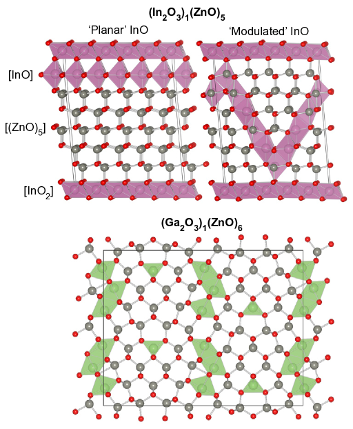
The multi-compounds (O3)m(ZnO)n with = In, Ga, and Al ( = integers) can be synthesized, for example, by solid state chemical reactions using stoichiometric proportions of the ZnO, In2O3, Ga2O3, Al2O3 binary compounds and heating at high temperatures (about K). The exact temperature required depends on the composition and the desired productsKimizuka-1995-170 ; Phani-1998-3969 ; Li-1999-355 ; Kim-2004-163 ; Michiue-2008-521 . A large number of syntheses have been performed; and crystal structures were first reported for = In and Ga, with different . The lowest energy structures identified for a number of these compounds are shown in Figure 1.
Except for the spinel structured compound ZnAl2O4, there have been limited reports for the synthesis of single crystal (Al2O3)(ZnO)n compounds for . The Zn-rich alloy was recently grown by pulsed laser deposition in the work of Yoshioka et al.yoshioka-014309 , where a superlattice structure was identified, which is consistent with the homologous crystal structure models developed for the In and Ga compounds, as later verified by electronic structure calculationsyoshioka-137 . There is growing evidence for the presence of the homologous phase in typical Al-doped ZnO samplesvinnichenko-141907 ; horwat-132003 , which can contribute to lower than expected electron carrier concentrations: excess electrons are compensated by additional oxygen incorporation in to the lattice.
IV.1.1 (In2O3)m(ZnO)n and (Ga2O3)m(ZnO)n
IZO was first synthesized by KasperKasper-1967-113 for , who showed that the compounds adopt layered structures and crystallise in rhombohedral or hexagonal crystal lattices. Two decades later, Cannard and Tilley confirmed Kasper’s results using X-ray diffraction (XRD) and high-resolution electron microscopy (HREM) experimentsCannard-1988-418 . Recently, Kimizuka et al.Kimizuka-1981-109 ; Kimizuka-1995-170 proposed that IZO is isostructural with LuFeO3(ZnO)n for Isobe-1994-332 . The crystal has the space group (rhombohedral lattice) when is odd and (hexagonal lattice) when is even. The In atoms form an InO2 octahedron layer, which are interconnected by (InZnn)On+1 layers. The In atoms in the (InZnn)On+1 unit were assumed to be randomly distributed on the metal sites, forming 5-fold trigonal bipyramidal polyhedraIsobe-1994-332 , while the Zn atoms were assumed to be located in tetrahedral sites surrounded by four O atoms. The formation of an InO2 octahedron layer was also confirmed by atomic-resolution Z-contrast experiments for In2O3(ZnO)nYan-1998-2585 . In contrast to the XRD studies,Kimizuka-1981-109 ; Kimizuka-1995-170 ; Moriga-1998-1310 recent HREM experimentsUchida-1994-146 ; Li-1998-347 ; Li-2000-543 ; Wolf-2007-549 have indicated that the In atoms in the (InZnn)On+1 layers form ordered modulated structures with a zig-zag shape.
So far, the synthesis of GZO has been reported only for , Phani-1998-3969 ; Kim-2004-163 ,Michiue-2008-521 ,Kimizuka-1995-170 and . Li-1999-355 To our knowledge, there is no report for . Experimental characterisation using XRD has found that GZO crystallizes in orthorhombic structures with space group for , and the ‘normal’ cubic spinel structure for . The internal structural parameters (atomic positions) have been reported only for Michiue-2008-521 ; however, it is important to note that the atomic number of Ga and Zn differs only by one unit, and hence, XRD alone cannot clearly distinguish between the Ga and Zn site occupation, i.e. it was assumed that Ga atoms occupy specific cation sites, while Zn occupy the remaining sites. The pioneering work reported by Michiue et al.Michiue-2008-521 provided a basis for the understanding of the atomic structure of GZO compounds; however, a number of questions remained to be solved at that time.
Recently, Da Silva et al.dasilva-255501 ; DaSilva-2009-214118 employed first-principles computational tools to address the mechanisms that lead to the formation of the layered IZO structures with the In-modulations in the (InZnn)On+1 layers and the atomic distribution of the Ga and Zn cations in the GZO lattice, which forms natural grain-boundaries. Below, we will summarize the most important results, which can be used as guidelines for a better understanding of these materials and other related oxide compounds.
The preference of In to form octahedron networks:
The In and O atoms in the bixbyite In2O3 structure are 6- and 4-fold coordinated,Marezio-1966-723 respectively, whereas both Zn and O atoms are 4-fold coordinated in the wz structure. In contrast to the In atoms, the Ga atoms in the monoclinic -Ga2O3 structure are separated into two groups composed of four distorted octahedron and four tetrahedron, while there are eight 3-fold and four 4-fold O atoms. In particular, a pair of octahedrons are surrounded by 6 tetrahedrons, which can be seen as a basic motif in -Ga2O3. For the simplest multi-compound structure, i.e. the high symmetry ZnO4 ( = In, Ga) spinel structure may also exist, in which the In, Zn, and O atoms are 6-, 4-, and 4-fold coordinated, respectively. The coordination environments observed for the In, Ga, Zn, and O atoms are related to the fact that In, Ga, and Zn have three, three, and two valence electrons, respectively, whereas oxygen always has a valence of , so the coordination environments are determined such that the octet rule for local charge neutrality is satisfied. Thus, it can be expected that In should prefer to form octahedrons, whereas Ga can form both octahedrons as well as tetrahedrons, even though both atoms have the same formal valence. To test this hypothesis, we investigate several IZO and GZO model structures.
Two types of 6-fold coordinated InO2 layers were calculated in IZO, namely, a non-octahedron structure and an octahedron structure. The octahedron structure is about 1 eV/InO2 lower in energy than the non-octahedron structure. This is consistent with the fact that the octahedron structure maximizes the atomic separation between the negatively charged O atoms. In the octehedron structure, the InO distances in the InO2 layers are in the range of Å, while the angle of OInO deviates by from the ideal value of . The smallest deviations () occur when O atoms in the corner of the octahedron are shared with Zn atoms. Thus, the binding of Zn to O at the corner of the InO2 octahedron layers stabilises the formation of an almost perfect In-O octahedron, whereas binding to In induces a larger distortion. These findings are consistent with the formation of distorted and perfect octahedron structures in the bixbyite In2O3 and the spinel In2ZnO4 structures, respectively. The observation that the In and O atoms in the InO2 layer form an octahedron structure is consistent with experimental observations.Kimizuka-1981-109 ; Giaquinta-1994-5 ; Isobe-1994-332 ; Kimizuka-1995-170 ; Yan-1998-2585
In contrast to the In atoms in IZO which is 6-fold coordinated, Ga atoms may exist at low coordination sites. For example, in the GZO structure proposed by Michiue et al.Michiue-2008-521 there are two cation sites (called and in Ref. Michiue-2008-521, ), which are 5- and 4-fold coordinated and were assumed to partially occupied by Zn atoms. We showed that the sites are empty and the sites are occupied by Ga atoms, while the remaining Ga atoms are distributed in 6-fold like sites. Similar to the -Ga2O3 structure, both Ga sites satisfy the octet rule. Thus, these results show clearly that In atoms have a stronger preference for octahedron sites in IZO than Ga atoms in GZO, which explains the formation of planar InO2 layers in IZO, whereas it is absent in GZO.
Inversion domain boundary formation in (Znn)On+1 layer:
As discussed above, the In atoms have a strong preference for octahedron sites, while the Ga atoms can occupy 6- and 4-fold sites. Thus, once the 6-fold In sites in the InO2 layer in IZO and the 4-fold Ga sites in GZO are occupied, the remaining In and Ga atoms must be distributed in the wz-like ZnO structure; however, all cation sites in the wurtzite structure are 4-fold and not 6-fold. Thus, changes must occur in the (Znn)On+1 layers in order to accommodate both In and Ga atoms and satisfy the electronic octet rule.
Furthermore, a number of structural features of IZO and GZO also contribute to the formation of an inversion domain boundary (IDB). For example, in IZO, the InO2 octahedron layers are connected by the wz-like (InZnn)On+1 layers, in which the O atoms at the corner of the octahedrons are connected to three In atoms in InO2 and one atom in the (InZnn)On+1 layer. Thus, the polarity at the bottom and top of the repeating unit is reversed, and hence, an IDB must exist in the (InZnn)On+1 layer to reverse this polarity. An InO2-like layer is not present in GZO; however, the distribution of the Ga atoms requires 6-fold like sites, which can be obtained through the formation of IDB in GZO. For both IZO and GZO cases, the IDB is located on the In and Ga atoms, which form 5-fold trigonal bipyramid structures with the surrounding O atoms in the (Znn)On+1 layers.
Stacking fault in the (Znn)On+1 layer:
It is important to realize that the formation of the IDB does not occur alone, i.e. 5-fold trigonal bipyramid sites cannot be created without disrupting the stacking sequence of the wz-like lattice. In order to preserve the hexagonality of wurtzite and without destroying the stable InO2 octahedron layer and the formation of the 4-fold Ga sites, one or more stacking faults must exist in the (Znn)On+1 layers. This has important consequences for determining the stable configurations of IZO. For example, the conventional hexagonal unit cells are composed of two, or three, InO2 layers separated by an equal number of (InZnn)On+1 layers in which is even or odd. This leads to a hexagonal primitive unit cell for even and rhombohedral (or monoclinic) for odd.
Modulation of atoms in the (Znn)On+1 layer:
As previously mentioned, to obey the material stoichiometry, a number of In and Ga atoms must adopt trigonal bipyramid structures with the surrounding O atoms; at low temperature, these motifs should form ordered configurations. The ionic radii of the In, Ga, and Zn atoms, i.e. 0.80 Å for In(III), 0.55 Å for Ga(III), and 0.60 Å for Zn(II),shannon-751 play a decisive role in determining the ordered structure that minimizes the internal strain of the IZO and GZO structures.
For example, model calculations demonstrated that the in-plane lattice constant of InO3 in the hexagonal InFeO3 structure Giaquinta-1994-5 is 8.4% larger than the in-plane lattice constant of ZnO in the wz structure. Thus, the In atoms must assume an ordered distribution in the (InZnn)On+1 layers to minimize the strain energy. Calculations for several different atomic configurations have identified that the In atoms are distributed in the cation sites following a zig-zag modulated structure in IZO, in which the modulation period is proportional to the number of ZnO units. Similarly, the Ga atoms are distributed in GZO to form a modulation, which match the one observed in IZO.
The modulation is composed of In/Ga and Zn atoms, which form trigonal bipyramidal structures. These results are consistent with experimental HREM studies, Uchida-1994-146 ; Li-1998-347 ; Li-2000-543 ; Wolf-2007-549 which observed clearly the formation of In-modulated structures in the (InZnn)n+1 layers for ZnO units and Li-1998-347 .
Electronic octet rule for the O in the (Znn)On+1 layers:
The minimum energy structure for ZnnOn+1 obeys the electronic octet rule (local charge neutrality), in which the presence of 5-fold Zn sites is fundamental for both IZO and GZO. The following environments were identified in IZO as fundamental for the electronic octet rule: the O atoms are surrounded by Zn(4) atoms, or Zn(4) + In(5) + Zn(5), or In(5) + Zn(5), where the numbers in parentheses indicate the integral coordination of the In and Zn atoms, so that each O atom always receives two electrons from neighbouring cations. Similar coordination environments are observed in GZO beyond of the 4-fold Ga sites. Furthermore, the octet rule is also satisfied for oxygen pairs along the in-plane In and Zn rows, e.g. , and for O atoms in the InO2 layers. Therefore, the local electrostatic environment plays a fundamental role in the stability of the (O3)m(ZnO)n compounds.
IV.1.2 (InO3)m(ZnO)n
One important requirement for technological applications of IZO is complete control of the electronic properties, e.g. band gap, and hence, several studies have been performed to obtain a procedure to tune the band gap of IZO for specific applications. One possible approach is the replacement of a percentage of In atoms by other trivalent species, e.g. Ga or Al atoms. Therefore, it is very important to understand the consequences of such substitutions on the IZO atomic structure. We observed that the ionic size of the In(III) and Ga(III) cations relative to Zn(II) plays an important role in the formation of the -modulations.
In our calculations, we assumed that half of the In atoms were replaced by Ga or Al atoms to form (InGaO3)m(ZnO)n and (InAlO3)m(ZnO)n, respectively. We found that the In atoms always form the InO2 layer, which is expected based on the high stability of In octahedron structures. Replacement of the In atoms in the InO2 layer by Ga or Al atoms and put In atoms in the ZnO layer, is highly energetically unfavourable. Thus, Ga and Al should replace the modulated In atoms in the ZnO layers. We also demonstrated that the in-plane lattice constant of InO3 in the hexagonal InFeO3 structureGiaquinta-1994-5 is larger by 8.4%, 2.4%, and 0.0% for = In, Ga, and Al, respectively, compared with the lattice constant of wz-ZnO. Therefore, for = In, a large strain exists in the ZnO and InO layers if the In atoms form a planar layer. The in-plane strain decreases for = Ga and is almost zero for = Al. Therefore, it is probable that the Al atoms are randomly distributed in IAZO, while in IGZO, modulated Ga ions might still be present.
IV.2 Amorphous multi-component oxides
In contrast to the high temperature associated with the synthesis of crystalline multi-component oxides, amorphous thin films can be grown by low temperature processing. Following an initial investigation by Hosono et al. on amorphous ternary oxideshosono-165 , the breakthrough for a-TCOs came from the report by Nomura et al.nomura-488 that the electron mobility of amorphous IGZO thin films could exceed 10 cm2V-1s-1, which is an order of magnitude greater than amorphous Si. IGZO has since become the most widely studied amorphous TCO, and has found application as an electron-injection-layer for solid-state lighting devicesnomura-488 ; nomura-1269 ; nomura-202117 .
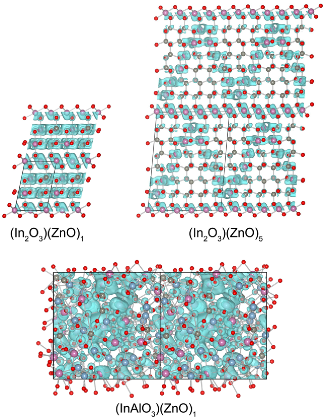
To simulate these low symmetry structures, a pseudo-cubic supercell of the crystalline structures was generated, which was subject to high temperatures under ab initio molecular dynamics until a solid to liquid phase transition was observed. Then, the liquid oxide was quenched, and the resulting structures were subject to local optimisation of both the internal positions and lattice constant. The full details of the approach employed can be found in Reference walsh-5119, . A snapshot of an amorphous structure is shown in Figure 2.
As previously shown, the crystal structures of the In and Zn containing oxides are defined by mixed In-O and Zn-O polyhedra (bipyramids and tetrahedra) present between InO2 octahedral planes. In the amorphous phases of IZO, IGZO and IAZO, the same local coordination motifs are maintained. To compare the local order in both phases, we have calculated both the effective coordination numberecn-1 ; ecn-2 and effective charge distribution for each ionwalsh-5119 . Even in the amorphous phase, the strong charge transfer between the metal cations and oxygen is preserved, driving the similar local coordination. While this is to be expected due to the large electro-negativity of oxygen, it is in contrast to covalent semiconductors, where amorphisation can lead to a large and significant local bond rearrangements that perturb the nearest neighbour environmentswooten-1392 .
The total energy difference between the crystalline and amorphous TCOs is of the order of 200 meV per f.u. in each system studied, which is expected based on the increased strain due to the disordered packing of the cation centred polyhedra on amorphisation. Despite their high energy, the a-TCOs remain metastable experimentally at standard temperatures as they do not have sufficient energy to overcome the large kinetic barriers required for recrystallization.
V Optical and Electronic Properties
The performance of electroceramics for TCO applications can be quantified by their electrical conductivity and optical absorption spectra. The former is related phenomenologically to the position of the electronic states on an absolute energy scale (band alignment), which influences the material’s doping limits, while the latter depends on the magnitude of the fundamental band gap, dipole selection rules for optical transitions, and carrier concentrations (e.g. the Moss-Burstein effectmoss-775 ; burstein-632 ).
Beyond the bulk material properties, the role of defects and non-stoichiometry in these oxides is also important in determining their performance for TCO applications. The theoretical framework for the accurate modelling of point defect formation exists, and the resulting free energies of formation for each defect charge state can be solved self-consistently to produce temperature dependant equilibrium defect and carrier concentrationskroger-1974 ; smith-2000 . Quantitative defect modelling techniques have not yet been applied to the case of the complex multi-component systems. The difficulty lies in the large number of inequivalent lattice positions, which must be calculated independently, as well as the lower lattice symmetry in comparison to the binary components; however, with the increase of high performance computing resources to the peta-scale, these issues will soon be overcome. Here, we can rationalise the material performance based on the bulk electronic changes observed in the multi-component systems.
V.1 Natural band offsets
The band offsets between semiconductors is one of the most fundamental properties for device physicsyu-05 . The absolute band edge positions of a material have a role in determining intrinsic doping limits,walukiewicz-123 ; zhang-1232 as well as their electrochemical propertiesxu-543 and interfacial electron transport. Experimentally, X-ray Photoemission Spectroscopy (XPS) can be used to measure the position of atomic-like core states, which provide a reference for the alignment between the valence bands of two or more systemskowalczyk-1605 . A theoretical approach has been developed in the same spirit, from which the ‘natural’ valence band offset of two compounds at their respective equilibrium positions can be calculatedwei-2011 ; wei-144 ; this approach has recently been revised to take into account the deformation of the core states with respect to volume changesli-212109 . The conduction band offsets can be inferred by adding the fundamental band gap to the computed valence band offset.
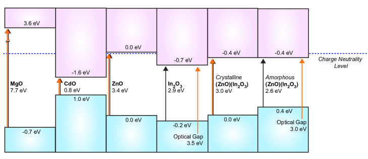
The natural band offsets derived for a number of oxide materials of interest are shown in Figure 3. The results match the recent alignment of the ultraviolet and inverse photoemission spectra for ZnO and In2O3kamiya-1061 . The observed trends are determined by a combination of shallow cation states (e.g. Cd 4 states raise the valence band of CdO), the degree of ionicity (e.g. efficient electron transfer produces a high electrostatic potential that lowers the valence band of MgO), and crystal structure (e.g. low coordination oxygen sites raise the valence band for amorphous IZO).
It can be observed from Figure 3 that In2O3 has the lowest conduction band level (highest electron affinity) of all the transparent oxides studied, which correlates with its ability to sustain high electron carrier concentrations that result in degenerate electron conduction. Indeed, recent experimental work has shown that the charge neutrality level, i.e. the Fermi energy at which oppositely charged defects can form spontaneously, of In2O3 lies well above the conduction bandking-116808 , which has been supported by calculations at the level of many-body perturbation theoryschleife-012104 ; further detail and implications of the charge neutrality level are discussed in work by King in this themed issueking-jpcm . While ZnO is a good -type semiconductor, the higher conduction band level limits its ability to be heavily electron doped. For large gap oxides such as Al2O3 and Ga2O3, electron doping will be even more difficult, with high degrees of ionic charge compensation expected to occurcatlow-nm . These effects have been summarised in a series of doping limit rules for semiconductorszhang-1232 ; wei-337 ; lany-045501 .
V.2 Forbidden optical transitions and carrier localisation in (In2O3)(ZnO)n
The principal reason why In2O3 remains a good TCO, despite its relatively small band gap, is that the band edge optical transitions are symmetry forbidden: it combines a small fundamental gap with a large optical band gap. Can this also be the case for the ternary In-containing compounds? For the homologous (In2O3)(ZnO)n series, we have shown that the lowest energy optical transitions from the valence to conduction bands are dipole allowed for all values of , as the top of the valence band state has large contribution from ZnO walsh-073105 . This explains the anomaly of why the apparent optical gap of In2O3 (ca. 3.6 eV)hamberg-3240 reduces to below 3.2 eV on the addition of ZnO to form IZOminami-971 ; moriga-312 ; taylor-90 .
For the IZO compounds, while the top of the valence band is more localised on the Zn-O network, the conduction band is localised on the In-O network, which follows from the band alignment of the binary materials (Figure 3). For = 1, the localisation is not significant as there are two mixed cation layers present between the In octahedra, and these contain an equal number of In and Zn ions. For higher values of , the number of intermixed layers increases, which raises the Zn:In ratio, and the band edge wavefunctions become more localised as a result. With the increased Zn concentration, an effective superlattice is formed and the charge carriers become confined in the InO2 octahedron network. The modulation of In ions through the ZnO layers makes a significant additional contribution to the conduction band, producing a modulated electron density distribution, as illustrated in Figure 2. The predicted carrier localization correlates well with the minimum of resistivity previously found for IZO samples with low Zn:In ratio, i.e. for the range minami-971 ; moriga-312 ; taylor-90 .
V.3 High performance of amorphous oxides
For the crystalline TCO compounds, the band gaps follow the clear trend of the group 13 binary oxides, increasing from In to Ga to Alwalsh-5119 . For the amorphous compounds, the same band gap trend is observed, but the magnitudes are lower compared to the crystalline structures. The differences arise from the series of bands situated at the top of the valence band. In the crystalline oxides, the lowest binding energy valence bands are dominated by O 2 states, and this is unchanged for the amorphous systems; however, the variation in electrostatic potential around each of the oxygen sites in the amorphous structures results in the spatial localisation of the valence wavefunctions. The contribution of the O 2 valence band to the sub band gap states has been confirmed through hard X-ray photoemission measurementsnomura-202117 , and is consistent with the band gap decrease observed for a-TCOskumar-073703 . As these states are concentrated in the Zn-rich regions (due to the lower binding energy shallow-core Zn 3 states), their contribution to the absorption of visible light is not significant because the conduction band is more localised on the group 13 cation side, and the resulting optical transition probabilities are low. As a result, the amorphous materials retain sufficient transparency in the visible region to be viable for TCO applications.
The electronic density of states predicted for the amorphous oxides has important consequences. Crucially for -type conductivity, the conduction band remains highly delocalised, which can be understood from the overlap between the disperse cation orbitals and the isotropic nature of the cation O 2 bondingnomura-488 ; medvedeva-57004 ; robertson-1026 : the overlap is largely unaffected by the long range structural disorder, which is illustrated in Figure 2.
As expected from their larger InO bond length compared to the other cations, In makes the largest contribution to the antibonding conduction band state. For IZO, two thirds of the cations are In, while for IGZO and IAZO, only one third In are present. As stated earlier, even for the lower concentration materials such as IAZO, the InO polyhedra form a combination of edge and corner sharing networks ensuring that the conduction band is appropriately spread over the entire amorphous network. This also explains why the amorphous, low indium concentration TCOs can exhibit good electrical transport properties: in the crystalline compounds, the InO networks become confined to two dimensional planes separated by the Zn and group 13 cations, while in the amorphous compounds, the indium ions become evenly distributed and hence offer improved isotropic carrier mobility.
While a-TCOs exhibit excellent -type conductivity, -type behaviour is not expected to be present due to the strong localisation of the upper valence band. The majority of known -type oxide semiconductors such CuAlO2 and SrCu2O2 are derived from Cu2O, where electron deficiency (hole formation) is facilitated by Cu oxidation, with carrier mobility along the linear O-Cu-O chains. Here, electrical carrier (polaron) mobility will be inhibited by the structural disorder on amorphisation. The absence of -type response has been reported experimentallynomura-202117 . The discovery of a high performance -type TCO material, either amorphous or crystalline, remains an open challenge in this field.
VI Discussion and Outlook
It is clear that the formation of multi-component oxides offers a way to tune the physicochemical properties associated with transparency and conduction. We have highlighted a number of rules that determine the structure formation of these complex materials. While the crystal structures of the binary oxide components are well described by the established principles of Paulingpauling-1010 ; pauling-1960 , for the multi-cation systems, features such as polarity inversion, stacking faults and partial site occupation arise. In terms of the electronic properties, for these -type materials, the key attribute is a delocalised conduction state, which can be maintained when a significant amount of In is present. The mixing of Ga and Al serves to both increase the band gap and the crystal stability, which can provide a means to control the stoichiometry and optical transmission, e.g. to provide a blue-shift in the optical band gap suitable for UV applications.
Despite these advances, a number of issues are still outstanding in the field of multi-component TCOs. Even in the ‘simpler’ binary metal oxide components, the origin and nature of conductivity remains a contentious issue. One common feature is that oxygen vacancies appear to be deep donor centres, with the neutral defects being stabilized by the strong Madelung potential of the lattice; conversely, metal interstitials generally act as shallow donors, but have higher formation energies. The role of hydrogen as an extrinsic donor impurity has been proposed for a number of TCO materialscox-2601 ; janotti-165202 ; king-081201 ; king-062110 , but it is highly unlikely to be the primary electron source. Fortunately, atomistic simulation techniques are becoming increasingly quantitative, and we can now predict defect formation energies with high accuracy, especially when temperature dependent contributions to the free energy are included. It is therefore anticipated that our understanding of the binary oxide systems will be solved in the near future, and that this understanding will transfer to the more complex multi-component systems.
One real limitation to transparent electronics is the absence of -type TCO materials, which are needed to form junctions for diodes and transistors. It appears that the performance of Cu-based compounds will not be sufficient for commercial applications. An alternative route to the use of Cu(I) is to form oxides of cations with filled bands such as Sn(II) or Bi(III)walsh-547 . Both SnO and BiVO4 have attracted recent attention for their -type conductivityogo-032113 ; vinke-83 . Moving away from pure oxide materials, forming solid-solutions with chalcogenides (S, Se and Te) may offer a way to increase hole stability by raising the valence band energy. In addition, the formation of hybrid materials containing -type inorganic networks and -type organic networks is also feasiblecheetham-58 , and we have performed exploratory work in this areawalsh-1284 ; walsh-2341 .
VII Conclusion
We have demonstrated the success of computational modelling techniques applied to the complex case of multi-component transparent conducting oxides. In the last decade, our understanding of the structural, electronic and optical properties of these materials has increased significantly. A number of fundamental ‘rules’ have been established relating to crystal structure formation, as well as the conductivity trends, which can provide a framework to enable, for example, a high-throughput computational screening of candidate compounds and stoichiometries. We note that despite these advances, many open questions remain in the field, especially concerning the microscopic origin of conductivity and the role of extended defects, such as dislocations and grain boundaries, which ensure that the field will remain active for the near future.
Acknowledgements.
A.W. would like to acknowledge funding from a Marie-Curie Intra-European Fellowship from the European Union under the Seventh Framework Programme, as well as membership of the UK’s HPC Materials Chemistry Consortium, which is funded by EPSRC (Grant No. EP/F067496). J.L.F.D.S. thanks the São Paulo Science Foundation (FAPESP). S.-H.W. is supported by the U.S. Department of Energy (DOE) under Contract No. DE-AC36-08GO28308; computing resources of the National Energy Research Scientific Computing Center were employed, which is supported by DOE under Contract No. DE-AC02-05CH11231.References
- (1) G. Thomas, Nature 389, 907 (1997)
- (2) P. P. Edwards, A. Porch, M. O. Jones, D. V. Morgan, and R. M. Perks, Dalton Trans. 15, 2295 (2004)
- (3) Y. Ohya, T. Yamamoto, and T. Ban, J. Am. Ceram. Soc. 91, 240 (2008)
- (4) J. H. W. DeWit, J. Solid State Chem. 20, 143 (1977)
- (5) J. H. W. DeWit, J. Solid State Chem. 8, 142 (1973)
- (6) R. L. Weiher, J. Appl. Phys. 33, 2834 (1962)
- (7) I. Hamberg, C. G. Granqvist, K. F. Berggren, B. E. Sernelius, and L. Engstrom, Phys. Rev. B 30, 3240 (1984)
- (8) P. D. C. King, T. D. Veal, D. J. Payne, A. Bourlange, R. G. Egdell, and C. F. McConville, Phys. Rev. Lett. 101, 116808 (2008)
- (9) C. Körber, V. Krishnakumar, A. Klein, G. Panaccione, P. Torelli, A. Walsh, J. L. F. Da Silva, S.-H. Wei, R. G. Egdell, and D. J. Payne, Phys. Rev. B 81, 165207 (Apr 2010)
- (10) A. Klein, C. Korber, A. Wachau, F. Sauberlich, Y. Gassenbauer, R. Schafranek, S. Harvey, and T.O.Mason, Thin Solid Films 518, 1197 (2009)
- (11) A. Walsh, J. L. F. Da Silva, S.-H. Wei, C. Körber, A. Klein, L. F. J. Piper, A. DeMasi, K. E. Smith, G. Panaccione, P. Torelli, D. J. Payne, A. Bourlange, and R. G. Egdell, Phys. Rev. Lett. 100, 167402 (2008)
- (12) A. Walsh, J. L. F. Da Silva, and S.-H. Wei, Phys. Rev. B 78, 075211 (2008)
- (13) A. Walsh and C. R. A. Catlow, J. Mater. Chem. 20, 10438 (2010)
- (14) S. Lany and A. Zunger, Phys. Rev. Lett. 98, 045501 (2007)
- (15) P. Ágoston, P. Erhart, A. Klein, and K. Albe, J. Phys.: Condens. Matter 21, 455801 (2009)
- (16) T. Tomita, K. Yamashita, Y. Hayafuji, and H. Adachi, Appl. Phys. Lett. 87, 051911 (2005)
- (17) P. Ágoston, K. Albe, R. M. Nieminen, and M. J. Puska, Phys. Rev. Lett. 103, 245501 (2009)
- (18) J. E. Medvedeva and C. L. Hettiarachchi, Phys. Rev. B 81, 125116 (2010)
- (19) O. F. Schirmer, J. Phys.: Condens. Matter 18, R667 (2006)
- (20) A. M. Stoneham, J. Gavartin, A. L. Shluger, A. V. Kimmel, D. M. Ramo, H. M. Ronnow, G. Aeppli, and C. Renner, J. Phys.: Condens. Matter 19, 255208 (2007)
- (21) X. Nie, S.-H. Wei, and S. B. Zhang, Phys. Rev. Lett. 88, 066405 (2002)
- (22) X. Nie, S.-H. Wei, and S. B. Zhang, Phys. Rev. B 65, 075111 (2002)
- (23) H. Kawazoe, M. Yasukawa, H. Hyodo, M. Kurita1, H. Yanagi, and H. Hosono, Nature 389, 939 (1997)
- (24) S. Saadi, A. Bouguelia, and M. Trari, Solar Energy 80, 272 (2006)
- (25) D. O. Scanlon, A. Walsh, B. J. Morgan, G. W. Watson, D. J. Payne, and R. G. Egdell, Phys. Rev. B 79, 035101 (2009)
- (26) T. Arnold, D. J. Payne, A. Bourlange, J. P. Hu, R. G. Egdell, L. F. J. Piper, L. Colakerol, A. De Masi, P.-A. Glans, T. Learmonth, K. E. Smith, J. Guo, D. O. Scanlon, A. Walsh, B. J. Morgan, and G. W. Watson, Phys. Rev. B 79, 075102 (2009)
- (27) M. N. Huda, Y. Yan, A. Walsh, S.-H. Wei, and M. M. Al-Jassim, Phys. Rev. B 80, 035205 (2009)
- (28) D. O. Scanlon, G. W. Watson, and A. Walsh, Chem. Mater. 21, 4568 (2009)
- (29) A. Kudo, H. Yanagi, H. Hosono, and H. Kawazoe, Appl. Phys. Lett. 73, 220 (1998)
- (30) K. G. Godinho, G. W. Watson, A. Walsh, A. Green, J. Harmer, D. Payne, and R. Egdell, J. Mater. Chem. 18, 2798 (2008)
- (31) D. O. Scanlon, B. J. Morgan, G. W. Watson, and A. Walsh, Phys. Rev. Lett. 103, 096405 (2009)
- (32) T. Minami, H. Sonohara, T. Kakumu, and S. Takata, Jpn. J. Appl. Phys. 34, L971 (1995)
- (33) M. P. Taylor, D. W. Readey, C. W. Teplin, M. F. A. M. van Hest, J. L. Alleman, M. S. Dabney, L. M. Gedvilas, B. M. Keyes, B. To, J. D. Perkins, and D. S. Ginley, Meas. Sci. Technol. 16, 90 (2005)
- (34) H. Hiramatsu, W.-S. Seo, and K. Koumoto, Chem. Mater. 10, 3033 (1998)
- (35) B. Kumar, H. Gong, and R. Akkipeddi, J. Appl. Phys. 98, 073703 (2005)
- (36) A. J. Leenheer, J. D. Perkins, M. F. A. M. van Hest, J. J. Berry, R. P. O’Hayre, and D. S. Ginley, Phys. Rev. B 77, 115215 (2008)
- (37) T. Moriga, T. Okamoto, K. Hiruta, A. Fujiwara, and I. Nakabayashi, J. Solid State Chem. 155, 312 (2000)
- (38) K. Nomura, H. Ohta, A. Takagi, T. Kamiya, M. Hirano, and H. Hosono, Nature 432, 488 (2004)
- (39) Y. Sun and J. Rogers, Adv. Mater. 19, 1897 (2007)
- (40) D.-H. Lee, Y.-J. Chang, G. Herman, and C.-H. Chang, Adv. Mater. 19, 843 (2008)
- (41) M. P. Taylor, D. W. Readey, M. F. A. M. van Hest, C. W. Teplin, J. L. Alleman, M. S. Dabney, L. M. Gedvilas, B. M. Keyes, B. To, J. D. Perkins, and D. S. Ginley, Adv. Funct. Mater. 18, 3169 (2008)
- (42) N. F. Mott, Conduction in non-crystalline materials, 1st ed. (Oxford Science Publications, Oxford, 1987)
- (43) A. Walsh, J. L. F. DaSilva, and S.-H. Wei, Chem. Mater. 21, 5119 (2009)
- (44) J. Robertson, Phys. Status Solidi B 245, 1026 (2008)
- (45) H. Hosono, K. Nomura, Y. Ogo, T. Uruga, and T. Kamiya, J. Non-Cryst. Solids 354, 2796 (2008)
- (46) H. Hosono, Thin Solid Films 515, 6000 (2007)
- (47) E. Fortunato, D. Ginley, H. Hosono, and D. C. Paine, MRS Bull. 32, 242 (2007)
- (48) C. A. Hoel, T. O. Mason, J.-F. Gaillard, and K. R. Poeppelmeier, Chem. Mater. 22, 3569 (2010)
- (49) C. R. A. Catlow, S. French, A. A. Sokol, A. Al-Sunaidi, and S. Woodley, J. Comp. Chem. 29, 2234 (2008)
- (50) S. Lany and A. Zunger, Phys. Rev. B 78, 235104 (2008)
- (51) A. Janotti and C. G. Van de Walle, Phys. Rev. B 76, 165202 (2007)
- (52) W. Kohn and L. J. Sham, Phys. Rev. 140, A1133 (1965)
- (53) P. Hohenberg and W. Kohn, Phys. Rev. 136, B864 (1964)
- (54) G. Kresse and J. Furthmüller, Phys. Rev. B 54, 11169 (1996)
- (55) M. Segall, P. Lindan, M. Probert, C. Pickard, P. Hasnip, S. Clark, and M. Payne, J. Phys.: Cond. Matter 14, 2717 (2002)
- (56) P. Giannozzi, S. Baroni, N. Bonini, M. Calandra, R. Car, C. Cavazzoni, D. Ceresoli, G. Chiarotti, M. Cococcioni, I. Dabo, et al., J. Phys.: Cond. Matter 21, 395502 (2009)
- (57) V. Blum, R. Gehrke, F. Hanke, P. Havu, V. Havu, X. Ren, K. Reuter, and M. Scheffler, Comp. Phys. Comm. 180, 2175 (2009)
- (58) R. M. Martin, Electronic Structure, 1st ed. (Cambridge University Press, Cambridge, 2004)
- (59) M. C. Payne, M. P. Teter, D. C. Allan, T. A. Arias, and J. D. Joannopoulos, Rev. Mod. Phys. 64, 1045 (1992)
- (60) S. M. Woodley and C. R. A. Catlow, Nat. Mater. 7, 937 (2008)
- (61) A. Walsh and S. M. Woodley, Phys. Chem. Chem. Phys. 12, 8446 (2010)
- (62) G. Trimarchi and A. Zunger, J. Phys.: Condens. Matter 20, 295212 (2008)
- (63) G. Hautier, C. Fischer, A. Jain, T. Mueller, and G. Ceder, Chem. Mater. 22, 3762 (2010)
- (64) D. M. Ceperley and B. J. Alder, Phys. Rev. Lett. 45, 566 (1980)
- (65) J. P. Perdew, K. Burke, and M. Ernzerhof, Phys. Rev. Lett. 77, 3865 (1996)
- (66) J. P. Perdew and A. Zunger, Phys. Rev. B 23, 5048 (1981)
- (67) J. P. Perdew and M. Levy, Phys. Rev. Lett. 51, 1884 (1983)
- (68) L. J. Sham and M. Schlüter, Phys. Rev. Lett. 51, 1888 (1983)
- (69) L. Hedin, Phys. Rev. 139, A796 (1965)
- (70) F. Cora, M. Alfredsson, G. Mallia, D. S. Middlemiss, W. C. Mackrodt, R. Dovesi, and R. Orlando, ”The Performance of Hybrid Density Functionals in Solid State Chemistry” in Structure and Bonding, 1st ed. (Springer, Berlin, 2004)
- (71) J. Heyd, G. E. Scuseria, and M. Ernzerhof, J. Chem. Phys. 118, 8207 (2003)
- (72) J. Paier, M. Marsman, K. Hummer, G. Kresse, I. C. Gerber, and J. G. Angyan, J. Chem. Phys. 124, 154709 (2006)
- (73) R. Bader, Atoms in Molecules: A Quantum Theory (Oxford University Press, New York, 1990)
- (74) E. Sanville, S. D. Kenny, R. Smith, and G. Henkelman, J. Comp. Chem. 28, 899 (2007)
- (75) M. Jansen and U. Wedig, Ange. Chemie 47 (2008)
- (76) C. R. A. Catlow and A. Stoneham, J. Phys. C 16, 4321 (1983)
- (77) U. Özgür, Y. I. Alivov, C. Liu, A. Teke, M. A. Reshchikov, S. Doğan, V. Avrutin, S.-J. Cho, and H. Morkoç, J. Appl. Phys. 98, 041301 (2005)
- (78) K. R. Kittilstved, W. K. Liu, and D. R. Gamelin, Nat. Mater. 5, 291 (2006)
- (79) A. Walsh, J. L. F. Da Silva, and S.-H. Wei, Phys. Rev. Lett. 100, 256401 (2008)
- (80) A. Walsh, J. L. F. Da Silva, and S.-H. Wei, Phys. Rev. Lett. 102, 159702 (2009)
- (81) O. M. Madelung, Semiconductors: Data Handbook, 3rd ed. (Springer, Berlin, 2004)
- (82) C. R. A. Catlow, Z. X. Guo, M. Miskufova, S. A. Shevlin, A. G. H. Smith, A. A. Sokol, A. Walsh, D. J. Wilson, and S. M. Woodley, Phil. Trans. Roy. Soc. A 368, 1923 (2010)
- (83) A. A. Sokol, S. A. French, S. T. Bromley, C. R. A. Catlow, H. J. J. van Dam, and P. Sherwood, Faraday Discuss. 134, 267 (2007)
- (84) I. Hamberg and C. G. Granqvist, J. Appl. Phys. 60, R123 (1986)
- (85) M. Marezio, Acta Crystallogr. 20, 723 (1966)
- (86) F. Fuchs and F. Bechstedt, Phys. Rev. B 77, 155107 (2008)
- (87) M. Passlack, E. F. Schubert, W. S. Hobson, M. Hong, N. Moriya, S. N. G. Chu, K. Konstadinidis, J. P. Mannaerts, M. L. Schnoes, and G. J. Zydzik, J. Appl. Phys. 77, 686 (1995)
- (88) S. Geller, J. Chem. Phys. 33, 676 (1960)
- (89) J. B. Varley, J. R. Weber, A. Janotti, and C. G. V. de Walle, Appl. Phys. Lett. 97, 142106 (2010)
- (90) B. Evans, J. Nucl. Mater. 219, 202 (1995)
- (91) T. Tomiki, Y. Ganaha, T. Shikenbaru, T. Futemma, M. Yuri, Y. Aiura, S. Sato, H. Fukutani, H. Kato, T. Miyahara, A. Yonesu, and J. Tamashiro, J. Phys. Soc. Jpn. 62, 573 (1993)
- (92) P. Thompson, D. Cox, and J. Hastings, J. Appl. Crystal. 20, 79 (1987)
- (93) J. Weber, A. Janotti, and C. V. de Walle, Microelect. Eng. 86, 1756 (2009)
- (94) C. R. A. Catlow, R. James, W. C. Mackrodt, and R. F. Stewart, Phys. Rev. B 25, 1006 (1982)
- (95) N. Hine, P. Haynes, A. Mostofi, and M. Payne, J. Chem. Phys. 133, 114111 (2010)
- (96) A. A. Sokol, A. Walsh, and C. R. A. Catlow, Chem. Phys. Lett. 492, 44 (2010)
- (97) D. R. Lide, CRC Handbook, 83rd ed. (CRC Press, London, 2002)
- (98) M. Orita, H. Ohta, M. Hirano, and H. Hosono, Appl. Phys. Lett. 77, 4166 (2000)
- (99) N. Kimizuka, M. Isobe, and M. Nakamura, J. Solid State Chem. 116, 170 (1995)
- (100) A. R. Phani, S. Santucci, S. Di Nardo, L. Lozzi, M. Passacantando, P. Picozzi, and C. Cantalini, J. Mater. Sci. 33, 3969 (1998)
- (101) C. Li, Y. Bando, M. Nakamura, K. Kurashima, and N. Kimizuka, Acta. Cryst. B55, 355 (1999)
- (102) J. S. Kim, H. L. Park, C. M. Chon, H. S. Moon, and T. W. Kim, Solid State Commun. 129, 163 (2004)
- (103) Y. Michiue, N. Kimizuka, and Y. Kanke, Acta Cryst. B64, 521 (2008)
- (104) S. Yoshioka, F. Oba, R. Huang, I. Tanaka, T. Mizoguchi, and T. Yamamoto, J. Appl. Phys 103, 014309 (2008)
- (105) S. Yoshioka, K. Toyoura, F. Oba, A. Kuwabara, K. Matsunaga, and I. Tanaka, Journal of Solid State Chemistry 181, 137 (2008)
- (106) M. Vinnichenko, R. Gago, S. Cornelius, N. Shevchenko, A. Rogozin, A. Kolitsch, F. Munnik, and W. Moller, Appl. Phys. Lett. 96, 141907 (2010)
- (107) D. Horwat, M. Jullien, F. Capon, J. Pierson, J. Andersson, and J. Endrino, J. Phys. D: Appl. Phys. 43, 132003 (2010)
- (108) K. Momma and F. Izumi, J. Appl. Cryst. 41, 653 (2008)
- (109) H. Kasper, Z. Anorg. Allg. Chem. 349, 113 (1967)
- (110) P. J. Cannard and R. J. D. Tilley, J. Solid State Chem. 73, 418 (1988)
- (111) N. Kimizuka and E. Takayama, J. Solid State Chem. 40, 109 (1981)
- (112) M. Isobe, N. Kimizuka, M. Nakamura, and T. Mohri, Acta. Cryst. C50, 332 (1994)
- (113) Y. Yan, S. J. Pennycook, J. Dai, R. P. H. Chang, A. Wang, and T. J. Marks, Appl. Phys. Lett. 73, 2585 (1998)
- (114) T. Moriga, D. D. Edwards, T. O. Mason, G. B. Palmer, K. R. Poeppelmeier, J. L. Schindler, C. R. Kannewurf, and I. Nakabayashi, J. Am. Ceram. Soc. 81, 1310 (1998)
- (115) N. Uchida, Y. Bando, M. Nakamura, and N. Kimizuka, J. Electron. Microsc. 43, 146 (1994)
- (116) C. Li, Y. Bando, M. Nakamura, M. Onoda, and N. Kimizuka, J. Solid State Chem. 139, 347 (1998)
- (117) C. Li, Y. Bando, M. Nakamura, and N. Kimizuka, Micron 31, 543 (2000)
- (118) F. Wolf, B. H. Freitag, and W. Mader, Micron 38, 549 (2007)
- (119) J. L. F. D. Silva, Y. Yan, and S.-H. Wei, Phys. Rev. Lett. 100, 255501 (2008)
- (120) J. L. F. Da Silva, A. Walsh, and S.-H. Wei, Phys. Rev. B 80, 214118 (2009)
- (121) M. Marezio, Acta Cryst. 20, 723 (1966)
- (122) D. M. Giaquinta, W. M. Davis, and H.-C. zur Loye, Acta Cryst. C 50, 5 (1994)
- (123) R. D. Shannon, Acta Crystallogr., Sect. A 32, 751 (1976)
- (124) H. Hosono, N. Kikuchi, N. Ueda, and H. Kawazoe, J. Non-Cryst. Solids 198-200, 165 (1996)
- (125) K. Nomura, H. Ohta, K. Ueda, T. Kamiya, M. Hirano, and H. Hosono, Science 300, 1269 (2003)
- (126) K. Nomura, T. Kamiya, H. Yanagi, E. Ikenaga, K. Yang, K. Kobayashi, M. Hirano, and H. Hosono, Appl. Phys. Lett. 92, 202117 (2008)
- (127) R. Hoppe, S. Voigt, H. Glaum, J. Kissel, H. P. Muller, and K. Bernet, J. Less-Common Met. 156, 105 (1989)
- (128) R. Hoppe, Angew. Chem. Internat. Edit. 9, 25 (1970)
- (129) F. Wooten, K. Winer, and D. Weaire, Phys. Rev. Lett. 54, 1392 (1985)
- (130) T. S. Moss, Proc. Phys. Soc. London Sect. B 67, 775 (1954)
- (131) E. Burstein, Phys. Rev. 93, 632 (1954)
- (132) F. A. Krger, The Chemistry of Imperfect Crystals: Volume 2, 2nd ed. (North-Holland, Amsterdam, 1974)
- (133) D. M. Smyth, The defect chemistry of metal oxides (Oxford University Press, Oxford, 2000)
- (134) P. Y. Yu and M. Cardona, Fundamentals of Semiconductors, 3rd ed. (Springer, Berlin, 2005)
- (135) W. Walukiewicz, Phys. B: Cond. Mat. 302-303, 123 (2001)
- (136) S. B. Zhang, S.-H. Wei, and A. Zunger, Phys. Rev. Lett. 84, 1232 (2000)
- (137) Y. Xu and M. A. Schoonenz, Am. Mineral. 85, 543 (2000)
- (138) S. P. Kowalczyk, J. T. Cheung, E. A. Kraut, and R. W. Grant, Phys. Rev. Lett. 56, 1605 (1986)
- (139) S.-H. Wei and A. Zunger, Appl. Phys. Lett. 72, 2011 (1998)
- (140) S.-H. Wei and A. Zunger, Phys. Rev. Lett. 59, 144 (1987)
- (141) Y.-H. Li, A. Walsh, S. Chen, W.-J. Yin, J.-H. Yang, J. Li, J. L. F. D. Silva, X. G. Gong, and S.-H. Wei, Appl. Phys. Lett. 94, 212109 (2009)
- (142) T. Kamiya and M. Kawasaki, MRS Bull. 33, 1061 (2008)
- (143) A. Schleife, F. Fuchs, C. Rödl, J. Furthmüller, and F. Bechstedt, Appl. Phys. Lett. 94, 012104 (2009)
- (144) P. D. C. King, J. Phys: Condens. Matter This Issue, C (2011)
- (145) C. R. A. Catlow, A. A. Sokol, and A. Walsh, In Preparation(2011)
- (146) S.-H. Wei, Comput. Mater. Sci. 30, 337 (2004)
- (147) Y. Z. Zhu, G. D. Chen, H. Ye, A. Walsh, C. Y. Moon, and S.-H. Wei, Phys. Rev. B 77, 245209 (2008)
- (148) A. Walsh, J. L. F. DaSilva, Y. Yan, M. M. Al-Jassim, and S.-H. Wei, Phys. Rev. B 7, 073105 (2009)
- (149) J. E. Medvedeva, Euro. Phys. Lett. 78, 57004 (2007)
- (150) L. Pauling, J. Am. Chem. Soc. 51, 1010 (1929)
- (151) L. Pauling, The nature of the chemical bond, 3rd ed. (Cornell University Press, Ithaca, New York, 1960)
- (152) S. F. J. Cox, E. A. Davis, S. P. Cottrell, P. J. C. King, J. S. Lord, J. M. Gil, H. V. Alberto, R. C. Vilão, J. Piroto Duarte, N. Ayres de Campos, A. Weidinger, R. L. Lichti, and S. J. C. Irvine, Phys. Rev. Lett. 86, 2601 (2001)
- (153) P. D. C. King, R. L. Lichti, Y. G. Celebi, J. M. Gil, R. C. Vilão, H. V. Alberto, J. Piroto Duarte, D. J. Payne, R. G. Egdell, I. McKenzie, C. F. McConville, S. F. J. Cox, and T. D. Veal, Phys. Rev. B 80, 081201 (2009)
- (154) P. D. C. King, I. McKenzie, and T. D. Veal, Appl. Phys. Lett. 96 (2010)
- (155) A. Walsh, Y. Yan, M. N. Huda, M. M. Al-Jassim, and S.-H. Wei, Chem. Mater. 21, 547 (2009)
- (156) Y. Ogo, H. Hiramatsu, K. Nomura, H. Yanagi, T. Kamiya, M. Hirano, and H. Hosono, Appl. Phys. Lett. 93, 032113 (2008)
- (157) I. Vinke, J. Diepgrond, B. Boukamp, K. de Vries, and A. Burggraaf, Solid State Ionics 6, 83 (1992)
- (158) A. K. Cheetham and C. N. R. Rao, Science 318, 58 (2007)
- (159) A. Walsh, J. Phys. Chem. Lett. 1, 1284 (2010)
- (160) A. Walsh and C. R. A. Catlow, ChemPhysChem 11, 2341 (2010)