Inelastic electron tunneling spectroscopy of a single nuclear spin
Abstract
Detection of a single nuclear spin constitutes an outstanding problem in different fields of physics such as quantum computing or magnetic imaging. Here we show that the energy levels of a single nuclear spin can be measured by means of inelastic electron tunneling spectroscopy (IETS). We consider two different systems, a magnetic adatom probed with STM and a single Bi dopant in a Silicon nanotransistor. We find that the hyperfine coupling opens new transport channels which can be resolved at experimentally accessible temperatures. Our simulations evince that IETS yield information about the occupation of the nuclear spin states, paving the way towards transport-detected single nuclear spin resonance.
Probing a single nuclear spin represents both the ultimate resolution limit of magnetic resonance imaging and a requirement in quantum computing proposals where the nuclear spin is used as a qubit. The idea of storing and manipulating information in nuclear spins goes back to quantum computing proposals based on P donors in SiKane (1998) and NMR quantum computing Gershenfeld and Chuang (1997). Because of their very small coupling to their environment, the nuclear spin coherence time is expected to be very long but, for the same reason, quantum measurement of a single nuclear spin remains a formidable task. Recent experimental breakthroughs have made it possible to perform single shot non-destructive measurement of a single nuclear spin by means of optically detected single spin magnetic resonance in NV centers in diamond Neumann et al. (2010).
Here we propose a setup based on inelastic electron tunneling spectroscopy (IETS) that would permit to probe the spin transitions of a single nuclear spin with a space resolution down to 1 outperforming in this particular regard the optical detection. Our proposal builds on recent progress to probe the spin of a single atom using two different strategies. On one side, Scanning Tunneling Miscrocope (STM) inelastic electron tunnel spectroscopy Heinrich et al. (2004); Hirjibehedin et al. (2006, 2007); Otte et al. (2008, 2009); Loth et al. (2010); Khajetoorians et al. (2010) which allow to measure the electron spin spectral function of a single magnetic atom Fernández-Rossier (2009) weakly coupled to a conducting substrate. On the other side, the fabrication of a Silicon nanotransitor where transport occurs through the electronic states of a single dopantLansbergen et al. (2010); Tan et al. (2010).
In STM-IETS experiment electrons tunnel between the tip and the conducting substrate going through the magnetic atom. As the bias voltage is increased, a new conduction channel opens whenever is larger than the energy of some internal excitation of the atom. In the case of isolated transition metal atoms with partially full shell, like Mn, Fe or Co, the only internal excitations available in the range of a few meV are spin excitations associated to the magnetocrystalline anisotropy Hirjibehedin et al. (2007); Fernández-Rossier (2009). In the case of the single dopant nanotransistor, the IETS of the electron spin in the donor level could be performed in the cotunneling regimeDe Franceschi et al. (2001).
Exchange coupling to nearby magnetic atoms affects significantly the spin excitation spectrum of the atom under the tip Hirjibehedin et al. (2006); Fernández-Rossier (2009); Otte et al. (2009); Loth et al. (2010). Hyperfine coupling to the nuclear spin should also result in a modification of the electronic spin spectral function which, in turn, could be probed in IETS provided that the spectral resolution is high enough. Our mechanism differs from earlier theory work Berman et al. (2001); Balatsky et al. (2006) proposing to detect the nuclear spin looking at its influence on the STM current noise spectrum. Their approach is based on previous experiments where electronic spin fluctuations are detected in the current noise spectraManassen et al. (1989), not in the conductivity spectra. Probing the spin transitions of a single nuclear spin would yield a completely unambiguous chemical identification of the atom and would be a first step towards transport-based quantum measurement of a single nuclear spin.
The rest of this letter is organized as follows. We first describe the general theory that relates nuclear spin flips to IETS transport features. Then we consider the archetypical case of a single Mn atom in a Cu2N surface Heinrich et al. (2004); Hirjibehedin et al. (2006, 2007); Loth et al. (2010). We find that the detection of the nuclear spin excitations could be done at mK, below the recently demonstrated 10mK experimental limit Song et al. (2010), and how the visibility can be enhanced driving the nuclear spin out of equilibrium. We then analyze the case of 209Bi in Silicon and we find it is an optimal system to observe single nuclear spin flips at temperatures up to 60mK.
The electronic spin and nuclear total angular momentum are described by a Hamiltonian whose eigenvalues and eigenvectors are denoted by and , where is the basis in which both electronic and nuclear spin have well defined projection along the axis. The spin mixing coefficients depend on the specifics of the Hamiltonian, described below, which includes hyperfine coupling, Zeeman coupling and magnetic anisotropy terms. The inelastic transport spectroscopy is sensitive to transitions between states and with excitation energy . The electronic spin is coupled to electrons in the electrodes, denoted as tip (source) and the surface (drain) in the STM (nanotransistor) geometry, through a Kondo-like HamiltonianAppelbaum (1967); Fernández-Rossier (2009); Fransson (2009); Delgado et al. (2010):
| (1) |
where both electrode conserving and electrode non-conserving exchange couplings are included. The operator creates an electron with spin and orbital quantum number , where labels the electrode and the wave vector. The index runs over , with and the Pauli matrices and the atom electronic spin operators respectively. The term (with and the identity matrix) corresponds to potential scattering. We assume that exchange is momentum independent, spin isotropic and electrode dependent: . Here are dimensionless parameters that account for the different coupling between the magnetic adatom and either the tip or the surfaceDelgado et al. (2010); Delgado and Fernández-Rossier (2010).
The inelastic current due to electronic-spin assisted tunneling can be expressedFernández-Rossier (2009) as a convolution of the electronic spin spectral function:
| (2) |
where denotes the average occupation of the state and . The inelastic current can be written as Fernández-Rossier (2009); Delgado and Fernández-Rossier (2010):
| (3) |
Here is the tunneling conductance, is the quantum of conductance and the density of states of the electrode at the Fermi level. The inelastic current associated to a single channel is given by , with and .
Importantly, has a step at that accounts for the characteristic lineshape. Thus, whenever the bias energy exceeds a transition energy between spin states with such that the initial state is occupied, , and the electronic spin flip transition is permitted, , the differential conductance has a step and has a peak (or a valley at negative bias) with a thermal broadeningLambe and Jaklevic (1968) of . Thus, the line-shape should be quite similar to the electronic spin spectral function . In the following we assume that the intrinsic broadening of the spin excitations, due for instance to their coupling to the conducting substrateDelgado et al. (2010); Gauyacq et al. (2010); Delgado and Fernández-Rossier (2010), is negligible compared to , as it happens in the case of Mn adatoms in Cu2N Loth et al. (2010); Gauyacq et al. (2010); Delgado and Fernández-Rossier (2010).
The occupation functions can differ substantially from those of equilibrium when the typical time elapsed between inelastic current events is shorter than the spin relaxation time Delgado et al. (2010); Delgado and Fernández-Rossier (2010). We determine the occupation functions by solving a master equationDelgado et al. (2010); Delgado and Fernández-Rossier (2010) that accounts for the dissipative dynamics of the current driven electronic spin interacting with the nuclear spin. Both energy and spin are exchanged between the electrons in the electrodes on one side, and the nuclear and electronic spin of the single atom on the other. The scattering events involve the creation or annihilation of an electron-hole either in the same electrode, in which case no current is involved, or in different electrodes. Thus, depends in general, on the voltage, the conductance and the temperature Delgado and Fernández-Rossier (2010).
We now address the main question of this letter: under which conditions would IETS reveal transitions that provide information about the nuclear spin state?. We first consider the case of a single Mn adatom in a Cu2N surface. This system has been widely studied experimentally and theoreticallyHirjibehedin et al. (2006, 2007); Fransson (2009); Fernández-Rossier (2009); Persson (2009); Loth et al. (2010); Delgado et al. (2010); Gauyacq et al. (2010); Delgado and Fernández-Rossier (2010) but the role of the nuclear spin has been overlooked so far. The single atom electronic spin can be described by means of a spin Hamiltonian,
| (4) |
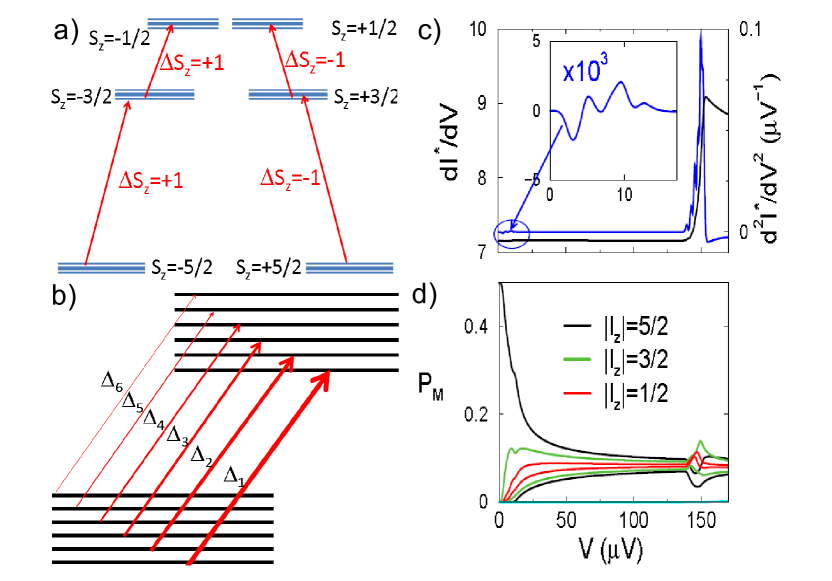
where eV and eV account for the uniaxial and in-plane anisotropy respectively, whereas the third term describes the electronic Zeeman coupling. At zero magnetic field the experimentalHirjibehedin et al. (2007) features a step at an energy of associated to electronic spin flip between the two ground states which neglecting , have and the first excited states, with , see Fig. 1(a). The only stable nuclear isotope of Mn is 55Mn and has a nuclear spin of , so that the electronic-nuclear system has 36 states in total. The hyperfine structure associated to the coupling between and has been resolved with EPR and NMR experiments that address ensembles of more than 1012 atoms, and can be described by a Heisenberg-type coupling. So, the spin Hamiltonian reads as
| (5) |
The strength of the hyperfine coupling depends both on the nuclear magnetic moment and on the shape of the electronic cloud, which is environment dependent. In the case of Mn, varies between 0.3 and 1eV Walsh et al. (1965). Here we take . The effect of the hyperfine coupling is to split each of the 6 electronic levels into 6 nuclear branches, as observed in Fig. 1a,b). The lowest electronic multiplet, corresponds to the , while the and branches are found approximately at and above.
The discussion can be simplified if we take advantage of the fact that so that the eigenstates of have, to zeroth order in and , well defined projection of the electronic () and nuclear () spin, although the numerical calculations are done with the exact states. The energies are approximately given by . We find two kind of transitions: low energy excitations with and higher energy excitations with .The former are found at small bias , where is the change in nuclear spin. Whereas these transitions yield very weak peaks in , shown in Fig. 1d), they contribute to drive the nuclear spin out of equilibrium, as seen in Fig. 3a).
In contrast, the electronic spin transitions between the electronic ground states and the first excited states that, to zeroth order, conserve the nuclear spin, occur at higher and have a much stronger signal (Fig. 1c,d) and 2). At their energies are given by so that, the hyperfine coupling splits the lowest energy line of the electronic spin spectral function into 6 lines separated by . In order to have a thermal broadening smaller than , must be reduced down to eV (mK), which would deplete the thermal occupation of the higher energy nuclear states within the electronic ground state, and the visibility of the corresponding spin excitations. In contrast, by decreasing the tip-atom distance Loth et al. (2010) it is possible to drive the system out of equilibrium and populate also the higher energy nuclear spin states at low temperatures, as shown in Fig. 1d), which makes it possible to observe all the transitions, as seen in Fig. 2 even at .
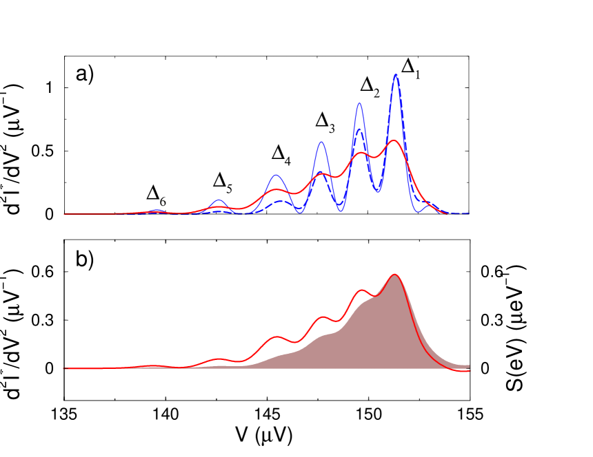
In figure 2b) we plot together with the the electronic spin spectral function , where the occupations evaluated at and the delta function replaced by . It is apparent that and are related. Importantly, the spin spectral function contains information not only about the energy levels of the joint nuclear-electronic spin, but also about the occupations of the states. Thus, the height of the can be correlated with the occupations of the nuclear spin states, outperforming current-noise spectroscopyBerman et al. (2001); Balatsky et al. (2006). This indicates that it would be possible to use IETS-STM as a detector in a magnetic resonance experiment, in analogy with the optically detected single spin magnetic resonance. This would permit to probe the magnetic field with subatomic spatial resolution and accuracy afforded by the linewidth of nuclear resonance experiment.
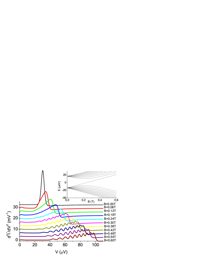
Nuclear spins with larger hyperfine coupling, like Yb, Er or Pr, Guillot-Noël et al. (2006); Ma et al. (2004) could be probed with IETS at higher temperatures than Mn. For instance 167Er3+ in Y2SiO5 Guillot-Noël et al. (2006) can have up to eV. The case of 232Bi in Silicon is particularly interesting. This system attracts a lot of interestMorley et al. (2010); George et al. (2010) in the context of quantum computing based on the nuclear spin of donorsKane (1998) where addressing the nuclear spin of a single dopant is required. The hyperfine coupling between the nuclear spin and the electronic spin of the donor state is quite large, (1.48GHz)Morley et al. (2010); George et al. (2010). The zero field Hamiltonian can be diagonalized in terms of the total angular operator , resulting in two multiplets (F=4,F=5) with energy . The zero field splitting is as large as eV, which could be resolved in IETS at mK. The evolution of the spectrum as a function of is shown in Fig. 3. A single Bi dopant in Si could be probed by single spin IETS-STM , recently demonstrated in semiconductor substratesKhajetoorians et al. (2010) or in a single dopant Silicon nanotransistor Lansbergen et al. (2010); Tan et al. (2010), both in the sequential regime, for which the curve yield the single electron spectral function, with peaks at every one of the 20 energy levels Fernández-Rossier and Aguado (2007), or in the cotunneling regime, described with the effective coupling (1) which yields information of the electronic spin spectral function. In figure 3 we show the evolution of the curves, as measured either with STM or in a nanotransistor in the cotunneling regime, for different values of at mK. It is apparent that transport permits to probe the spin-flip transitions between the Zeeman-split states of the joint electron-nuclear spin system.
In summary, we propose an experimental approach to probe a single nuclear spin using IETS of the hyperfine structure of the electronic spin excitations, extending thereby the range of applicability of IETS. Our simulations show that this technique yields information both about energy levels and the occupation of the nuclear spin states of a 55Mn adatom probed with a STM at mK. In the case of a single 232Bi dopant in a Si nanotransistor, the hyperfine structure could be detected at mK, well within range of current state of the art.
We acknowledge fruitful discussions with C. Untiedt, C. F. Hirjibehedin and A. F. Otte. This work was supported by MEC-Spain (MAT07-67845, FIS2010-21883-C02-01, Grants JCI-2008-01885 and CONSOLIDER CSD2007-00010) and Generalitat Valenciana (ACOMP/2010/070).
References
- Kane (1998) B. Kane, Nature 393, 133 (1998).
- Gershenfeld and Chuang (1997) N. A. Gershenfeld and I. L. Chuang, Science 275, 350 (1997).
- Neumann et al. (2010) P. Neumann, J. Beck, M. Steiner, F. Rempp, H. Fedder, P. R. Hemmer, J. Wrachtrup, and F. Jelezko, Science 329, 542 (2010).
- Heinrich et al. (2004) A. J. Heinrich, J. A. Gupta, C. P. Lutz, and D. M. Eigler, Science 306, 466 (2004).
- Hirjibehedin et al. (2006) C. F. Hirjibehedin, C. P. Lutz, and A. J. Heinrich, Science 312, 1021 (2006).
- Hirjibehedin et al. (2007) C. Hirjibehedin, C.-Y. Lin, A. Otte, M. Ternes, C. P. Lutz, B. A. Jones, and A. J. Heinrich, Science 317, 1199 (2007).
- Otte et al. (2008) A. F. Otte, M. Ternes, K. von Bergmann, S. Loth, H. Brune, C. P. Lutz, C. F. Hirjibehedin, , and A. J. Heinrich, Nature Physics 4, 847 (2008).
- Otte et al. (2009) A. F. Otte, M. Ternes, S. Loth, C. P. Lutz, C. F. Hirjibehedin, and A. J. Heinrich, Phys. Rev. Lett. 103, 107203 (2009).
- Loth et al. (2010) S. Loth, K. von Bergmann, M. Ternes, A. F. Otte, C. P. Lutz, and A. J. Heinrich, Nature Physics 6, 340 (2010).
- Khajetoorians et al. (2010) A. A. Khajetoorians, B. Chilian, J. Wiebe, S. Schuwalow, F. Lechermann, and R. Wiesendanger, Nature 467, 1084 (2010).
- Fernández-Rossier (2009) J. Fernández-Rossier, Phys. Rev. Lett. 102, 256802 (2009).
- Lansbergen et al. (2010) G. P. Lansbergen, G. C. Tettamanzi, J. Verduijn, N. Collaert, S. Biesemans, M. Blaauboer, and S. Rogge, Nano Letters 10, 455 (2010).
- Tan et al. (2010) K. Y. Tan, K. W. Chan, M. Mottonen, A. Morello, C. Yang, J. v. Donkelaar, A. Alves, J.-M. Pirkkalainen, D. N. Jamieson, R. G. Clark, et al., Nano Letters 10, 11 (2010).
- De Franceschi et al. (2001) S. De Franceschi, S. Sasaki, J. M. Elzerman, W. G. van der Wiel, S. Tarucha, and L. P. Kouwenhoven, Phys. Rev. Lett. 86, 878 (2001).
- Berman et al. (2001) G. P. Berman, G. W. Brown, M. E. Hawley, and V. I. Tsifrinovich, Phys. Rev. Lett. 87, 097902 (2001).
- Balatsky et al. (2006) A. V. Balatsky, J. Fransson, D. Mozyrsky, and Y. Manassen, Phys. Rev. B 73, 184429 (2006).
- Manassen et al. (1989) Y. Manassen, R. J. Hamers, J. E. Demuth, and A. J. Castellano Jr., Phys. Rev. Lett. 62, 2531 (1989).
- Song et al. (2010) Y. J. Song, A. F. Otte, Y. Kuk, Y. Hu, D. B. Torrance, P. N. First, W. A. de Heer, H. Min, S. Adam, M. D. Stiles, et al., Nature 467, 185– (2010).
- Appelbaum (1967) J. A. Appelbaum, Phys. Rev. 154, 633 (1967).
- Fransson (2009) J. Fransson, Nano Lett. 9, 2414 (2009).
- Delgado et al. (2010) F. Delgado, J. J. Palacios, and J. Fernández-Rossier, Phys. Rev. Lett. 104, 026601 (2010).
- Delgado and Fernández-Rossier (2010) F. Delgado and J. Fernández-Rossier, Phys. Rev. B 82, 134414 (2010).
- Lambe and Jaklevic (1968) J. Lambe and R. C. Jaklevic, Phys. Rev. 165, 821 (1968).
- Gauyacq et al. (2010) J.-P. Gauyacq, F. D. Novaes, and N. Lorente, Phys. Rev. B 81, 165423 (2010).
- Persson (2009) M. Persson, Phys. Rev. Lett. 103, 050801 (2009).
- Walsh et al. (1965) W. M. Walsh, J. Jeener, and N. Bloembergen, Phys. Rev. 139, A1338 (1965).
- Guillot-Noël et al. (2006) O. Guillot-Noël, P. Goldner, Y. L. Du, E. Baldit, P. Monnier, and K. Bencheikh, Phys. Rev. B 74, 214409 (2006).
- Ma et al. (2004) H. Ma, , and F. Yang, At. Data and Nuc. Data Tables 86, 18 (2004).
- Morley et al. (2010) G. W. Morley, M. Warner, A. M. Stoneham, P. T. Greenland, J. van Tol, C. W. M. Kay, and G. Aeppli, Nature Materials 9, 725– (2010).
- George et al. (2010) R. E. George, W. Witzel, H. Riemann, N. V. Abrosimov, N. Nötzel, M. L. W. Thewalt, and J. J. L. Morton, Phys. Rev. Lett. 105, 067601 (2010).
- Fernández-Rossier and Aguado (2007) J. Fernández-Rossier and R. Aguado, Phys. Rev. Lett. 98, 106805 (2007).