Stability of boron nitride bilayers: Ground state energies, interlayer distances, and tight-binding description
Abstract
We have studied boron nitride monolayer and bilayer band structures. For bilayers, the ground state energies of the different five stackings are computed using DFT in order to determine the most stable configuration. Also, the interlayer distance for the five different types of stacking in which boron-nitride bilayers can be found is determined. Using a minimal tight binding model for the band structures of boron nitride bilayers, the hopping parameters and the onsite energies have been extracted by fitting a tight binding empirical model to the DFT results.
pacs:
73.21.Ac, 73.63.Bd, 81.05.ueI Introduction
It was shown, since the early days of graphene research, that other layered materials can be exfoliated by micromechanical cleavage, following exactly the same procedure used to isolate graphene from graphite, giving birth, in this way, to new two-dimensional crystals, which will trigger, with certainty, new scientific investigations. Novoselov2005 Among these new materials there are several dichalcogenides, complex oxides, and boron nitride. It was also shown that these new two-dimensional forms of condensed matter show high crystal quality and macroscopic continuity. Novoselov2005
This new world of two-dimensional crystals is still much unexplored, both in what concerns the fundamental properties of these systems and their potential applications. Chief among these two-dimensional crystals, and excluding graphene for obvious reasons, boron nitride is emerging as a system which is finding applications as a scaffold for graphene in electronic devices. The fact that boron nitride is an insulator, having a large energy gap ( eV), together with its high degree of purity makes it a perfect membrane to isolate graphene from the imperfect gate dielectrics used so far. Since both systems, that is, graphene and boron nitride, interact weakly, two-dimensional crystals of the latter can be used as a buffer layer between a substrate and graphene, leaving its intrinsic electronic properties unafected by disorder associated with the dielectric surface. As a consequence, large electronic mobilities, of the same order of magnitude of those found in suspended graphene samples, have been measured in graphene on top of boron nitride. Dean2010 Graphene devices on hexagonal BN (-BN) have been shown to exhibit enhanced mobility, reduced carrier inhomogeneity, and reduced intrinsic doping, in comparison with graphene laying directly on top SiO2.Dean2010 Additionally, this new experimental setup allowed the measurement of the fractional quantum Hall effect using the four probes geometry, exposing a buried panoply of fractional filling factors, still waiting for deep fundamental justification. Other applications of BN can be envisioned, ranging from spacers to tunneling barriers.
Since these first applications of BN in fundamental research that the interest in single layer boron nitride (sBN) has been increasing steadily. In the recent past several experimental studies have been performed, Dean2010 ; Han2008 ; Meyer2009 ; Warner2010 ; Lee2010 ; Gorbachev2010 ; Song2010 including TEMHan2008 ; Meyer2009 ; Warner2010 and AFMLee2010 characterization of the material’s surface, optical and RamanGorbachev2010 spectroscopy, and intentional damage sBN’s surface.Meyer2009 ; Song2010 The main experimental approaches for producing sBN have been both mechanicalNovoselov2005 ; Meyer2009 ; Dean2010 ; Lee2010 and chemicalWarner2010 exfoliation. Others chemical methods are also available now.Han2008 ; Song2010 In addition to the discovery that sBN is an excellent substrate for graphene electronic devices, Dean2010 the fabrication of large area (several cm2) BN layers,Song2010 opens the possibility of mass production of this new two dimensional material, at the time of writing quite an expensive one.
In parallel to the experimental investigations, some theoretical studies on sBN and bilayer boron nitride (bBN) have been performed; Topsakal et al.Topsakal2008 made a density functional theory (DFT) study of the electronic, magnetic, and elastic properties of sBN and boron nitride nanoribbons. Giovannetti et al.Giovannetti2007 studied graphene on the top of -BN by DFT. These authors concluded that graphene opens a small gap for three orientations of graphene on the top of -BN, and that the most stable orientation was an AB stacking with the carbon atoms on the top of the boron atoms. Following the investigations by Giovannetti et al., Sławińska et al.Slawinska2010 studied graphene AB stacking on a sBN, using both tight-binding (TB) and DFT. They confirmed the opening of the gap and fitted the TB parameters to the DFT calculations. The difficulty with the aforementioned calculations is the fact that they assume graphene and sBN unit cells of the same size and perfectly oriented. We note in passing that the opening of a gap in graphene’s spectrum, when this material is laying on top of sBN, has been speculated to exist in the past and the transport properties of graphene under these conditions have been computed. zecarlos
Despite the above theoretical studies, it is however experimentally known that graphene on the top of sBN has in general a random crystallographic orientation, that is, there is no preferential orientation of graphene’s lattice relatively to that of sBN. Dean2010 In addition, no energy gap in graphene’s spectrum has been measured so far. Dean2010
Marom et al.Marom2010 studied the interlayer sliding of one layer of BN on the top of another layer of BN using DFT with van der Walls corrections. They found that the lower energy configurations (AA′ and AB) of bBN differ in energy by an amount smaller than the accuracy limits of their calculations.
In this paper we investigate the structural nature of the ground state of boron nitride bilayers using density functional theory. We consider the different possible stacking of the individual BN planes, compute their energy ground states and band structures, and fit the TB hopping parameters and on-site energies to the DFT results. Graphene bilayer can have two types of stacking: AA and AB (Bernal stacking), with the AB structure being the most stable one. BN bilayers have richer structural possibilities; given that there are two types of atoms, there are five possible bilayer stacking: two AA and three AB. Experiments show that both types of stacking exist when one considers multilayer BN.Warner2010 It is then important to clarify what can be expected in what concerns the energetic stability of the different stacking when one takes a bilayer as an isolated system.
II A minimal tight-binding model for bilayer boron nitride
Since we have in mind possible applications where both graphene and boron nitride two-dimensional crystals are brought into close contact with each other, we will be most interested in the energy bands due to the hybridization of the orbitals alone, the so called bands. The bands of BN can then be studied using an empirical tight-binding approach. The goal is simple: using DFT methods we will parametrize the tight-binding hopping and onsite energies of boron nitride layers, which can latter be used for microscopic calculations, such as tunneling properties.
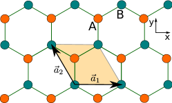
In Fig. 1 we represent the unit cell of a single layer of boron nitride with the primitive vectors and , both of length . The minimal tight binding model for a sBN has three parameters only: the hopping among nearest neighbor atoms and the onsite energies at the boron and the nitrogen atoms (in fact, one of these two onsite energies can be taken as a reference energy, and one ends up with two fitting parameters only). According to this simple model, the Hamiltonian for the electrons in the bands of sBN can be written as
| (1) |
where is the energy at the boron site, is the energy at the nitrogen site, and
| (2) |
The wave vector in the Brillouin zone is written as and the eigenvalues of Hamiltonian (1) are given by
| (3) |
where is the energy in the middle of the gap and is the energy gap. Slawinska2010
Using the above defined tight binding model one has three parameters that one needs to adjust: the hopping parameter , the band gap , and the middle gap energy , which can conveniently be chosen to be zero. These parameters can be found by adjusting Eq. (3) to the band structure of sBN computed from first principles.
For bilayer boron nitride, our minimal model includes, in addition to the one given above, an interlayer hopping parameter between the two atoms that are directly on top of each other. Hopping between atoms located at larger distances can be added to the model, at the expenses of having more fitting parameters. If one wants to fit accurately at the same time the valence and the conduction bands, adding these extra hoppings is strictly necessary. However, it is known that conduction bands in insulators are not well described by DFT calculations and thus we have found not to be necessary to go beyond this minimal model.
Five different structures of BN bilayers can exist in principle, assuming that either the atoms are located exactly on top of each other or at the center of the hexagons (we are excluding, for example, twisted bilayersJLS ); the five structures are represented in Fig. 2 (in the text that follows we will be referring to the different structures of BN bilayers by the notation introduced in that figure, which refer to the possible types of stacking).
AA  AA′
AA′ 
A′B  AB′
AB′ 
AB 

The AA and AA′ stacking (see Fig. 2) differ on what type of atoms are superimposed: in the AA case, atoms of the same type are superimposed, while in the AA′ case the boron atoms are on top of the nitrogen atoms and vice-versa. The A′B stacking has the nitrogen atoms superimposed on the two layers and a boron atom at the center of the hexagon, while AB′ stacking has the boron atoms superimposed on the two layers and a nitrogen atom at the center of the hexagon. The AB stacking has atoms of different types superimposed on the two layers and a boron atom at the center of the hexagon in one of the layers, while on the other layer is a nitrogen atom that is at the center of the hexagon. The differences among these fives possibilities should be clear from a close inspection of Fig. 2.
For boron nitride bilayers one finds that only two different Hamiltonians need to be written, since they describe all the five possible stacking (see Fig. 2) of bBN, after the appropriate changes. Therefore we have:
| (4) |
for the first two stacking in Fig. 2 (AA and AA′), and
| (5) |
for the remaining three cases in the same figure (AB, AB′ and A′B). In the last two Hamiltonians , , and are the energies at sites 1 to 4, two of which are boron atoms and the other two are nitrogen atoms. Atoms in the same plane are of different type implying that and . The parameter is the hopping between planes and is the same expression as in Eq. 2. Each of these Hamiltonians give four bands.
For the Hamiltonian (4), cases AA and AA′, the four energy bands can be written as:
| (6) |
where and have the same definition as above. For the Hamiltonian (5) we have to consider two different cases. The first one when and , meaning that there are two atoms of the same type (belonging to different layers; cases AB′ and A′B) on top of each other; in this case the energy eigenvalues read:
| (7) |
Note that for the case AB′ and for the case A′B. The second case happens when and , where the atoms on top of each other are of different types; in this case the energy eigenvalues are given by:
| (8) |
In equations (6), (7), and (8) there are four parameters which one needs to adjust: , which can be set to zero, , , and . In the bilayer, is not the energy gap, although it has the same definition as in the monolayer (see above). Having described the TB model for bBN, it is necessary to perform first principle calculations in order to determine the bands of these systems. Once this is done the TB bands are fit to the ab-initio results and the TB parameters defined above are extracted.
The density functional theory calculations were performed with an ab-initio spin-density functional code (aimpro).Rayson2008 We have used the GGA in the scheme of Perdew, Burke, and Ernzerhof.Perdew1996 Lower states (core states) were accounted for by using the dual-space separable pseudopotentials by Hartwigsen, Goedecker and Hutter.Hartwigsen1998 The valence states are expanded over a set of , , and like localized Cartesian-Gaussian Bloch atom-centered functions. In the framework of DFT calculations, the Brillouin-zone (BZ) was sampled for integrations according to the scheme proposed by Monkhorst-Pack.Monkhorst1976 The -point sampling was and both the atoms and the unit cell parameter were relaxed iteratively in order to find the equilibrium positions and size of the primitive cell. A supercell with hexagonal symmetry was used; the parameter was varied to find the equilibrium lattice constant, while the parameter was kept at 60 a.u.
III DFT results and tight binding fits of the energy spectrum of monolayer and bilayer boron nitride
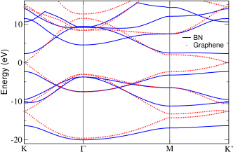
Boron nitride monolayers have very different electronic properties from those of graphene, since the broken symmetry of the and sub-lattices necessarily precluded the existence of Dirac cones at the corners of the Brillouin zone, creating a large band gap (larger than 5 eV) in the BN band structure.Han2008 Except for this vital difference, the rest of the electronic band structure of sBN resembles that found for graphene. The gap is at the -point and not at the -point (as in usual semiconductors) and, except for that particular zone in k-space, the shape of the bands of BN is similar to that of graphene bands. This is clearly shown in Fig. 3, where the band structure of the boron nitride single layer is shown superimposed on the band structure of graphene for comparison. The lattice parameter we have obtained for BN is Å, in good agreement with the value measured experimentally,Han2008 and for graphene we have found Å, giving a lattice mismatch of the order of 2% between the lengths of the primitive vectors of both crystal structures.
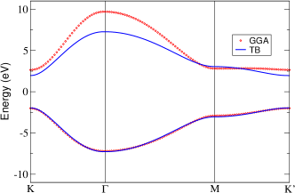
The parameters of Eq. (3) were adjusted to the orbitals of the valence band only, since DFT is more accurate for occupied states. The fitting was done to all the band in the line, unlike the fit done in Ref. [Slawinska2010, ]. In this latter work the bands were fit near the -point only. The curves resulting from fitting Eq. (3) to the ab initio data are shown in Fig. 4. The fitting to the valence band is excellent, but the resulting parameters do not give a perfect fit to the conduction band, although the TB conduction band does follow the same trend as that obtained from the ab-initio calculation, as it should be. Given that DFT calculations results in conduction and valence bands that are not particle-hole symmetric (for example, one has the width of the conduction band greater than that of the valence band), and that Eq. (3), by construction, preserves that symmetry, the tight binding model considering only a nearest neighbor hopping parameter will never fit both bands at the same time. The tight-binding parameters obtained from fitting the ab-initio bands are eV and eV, and the best fit is plotted in Fig. (4). The number we have obtained for is different from the one (=2.79 eV) obtained in Ref. Slawinska2010, and also from that obtained by the same group in a more recent work (=2.28 eV).Slawinska2010-1 In these two works the fitting was done only near de -point, and considering both valence and conduction bands, which is, most likely, the reason for the discrepancy between ours and the latter resultSlawinska2010-1 by those authors. We note that in their most recent workSlawinska2010-1 those authors have found a value for closer to the one we are reporting here. Our result for also agrees very well with the one we have obtained for the bBN (see Table 3); this is an important consistency check for our calculations.
We now turn to the study of the electronic spectrum of boron nitride bilayers. In our DFT calculations the primitive vector length was let to relax for all stackings and its final value was found to be Å for all the cases represented in Fig. 2; the area of primitive cell size remains essentially unchanged for the five types of stacking considered here. The situation is different in what concerns interlayer distances, as expected. Table 1 summarizes the results: if different types of atoms are superimposed, the two planes are closer than if the atoms are of the same type, since the chemical bonds of the type boron-nitrogen are preferred (leading to lower energy states), whereas boron-boron and nitrogen-nitrogen bonds are not. The two most stable stackings (AA′ and AB) have the same interplane distance. The interplane distances calculated here are consistent, although somewhat larger, than the experimentally measured value, which is Å.Warner2010 ; Han2008
| Sample | Atoms | (Å) |
|---|---|---|
| AA | B-B | 3.75 |
| AA | N-N | 3.75 |
| AA′ | B-N | 3.57 |
| AB | B-N | 3.57 |
| A′B | N-N | 3.72 |
| AB′ | B-B | 3.60 |
Taking the most stable stacking (lowest ground state energy) as a reference (AB stacking), the energy difference (per unit cell) of the corresponding ground states of the different stackings are given in Table 2. The AA stacking is the most energetic, followed by the A′B one, in which case the nitrogen atoms are on the top of each other. It is interesting that the most stable stacking is not the AA′ stacking as found for bulk BN,Terrones2007 but the AB stacking instead, as found for bilayer graphene and graphite. These results are consistent with those obtained in Ref. Marom2010, . As in that reference, the difference between the ground state energies of the AA and A′B stacking is very small, meaning, in practice, that both types of stacking can exist; in fact, both have been observed experimentally.Warner2010
| (meV) | (eV) | degeneracy | |
|---|---|---|---|
| AA | 13.5 | 4.23 | yes |
| AA′ | 0.4 | 4.69 | no |
| AB | 0.0 | 4.60 | no |
| A′B | 10.5 | 4.52 | yes (c.b.) |
| AB′ | 3.0 | 4.29 | yes (v.b.) |
Table 2 also shows the band gaps for all the bilayers band structure. The differences among them are small, reflecting the similarity of the band structure of these systems, both qualitatively and quantitatively. The differences in the band structure of the different types of bilayers are only noticeable near the and points, as can be seen in Fig. 5.
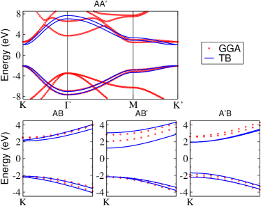
Figure 5 shows the full band structure of AA′ bilayer and the details of the electronic band structure near the -point for the others bilayer stackings, ploting both the DFT calculations and the tight binding fits. The tight-binding parameters for each bilayer represent in Fig. 2, , and , were adjusted such that Eqs. (6), (7), and (8) gave the best possible fit to the corresponding band structures as calculated by DFT. Only the valence band fits are accurate, since they are more reliable on DFT calculations than the conduction bands (a consequence of the fact that conduction bands have no electronic density in insulators). The TB conduction bands, as resulting from the fitting to the valence bands, are not in quantitatively good agreement with the DFT calculations, but qualitatively do show the same features. The resulting parameters are shown in table 3. It can be seen in Fig. 5 that the fits to the ab-initio bands are well described by the tight binding model using the parameters given in Table 3. As in the case of boron nitride monolayer, the tight binding valence bands describe quite well the bands calculated by DFT.
Although the three bottom panels of Fig. 5 may not give a clear impression of the good quality of the fit of the valence bands, given the scales of the figures, the fits are as good as that seen in the top panel of the same figure, where the full band structure of the AA′ bilayer is shown. For this reason, the full band structure is plotted only for the AA′ stacking, while for the other cases only the details of the band structure close to the are shown.
| (eV) | (eV) | (eV) | |
|---|---|---|---|
| AA′ | 4.08 | 2.36 | 0.32 |
| AB | 4.19 | 2.37 | 0.60 |
| A′B | -3.91 | 2.34 | 0.25 |
| AB′ | 4.32 | 2.38 | 0.91 |
The values found for the intralayer hopping parameter are very similar for the different stackings, as are the onsite energies at the boron and nitrogen atoms; this is expected since the intralayer hopping should be about the same for all stackings as well as for a BN monolayer, and indeed it is.
The valence and conduction bands are degenerated at the -point for the AA′ bilayer. For the AB stacking, there is a slight energy difference (at the -point) between the two valence and conduction bands, and therefore no degeneracy is observed. For the A′B bilayer the conduction bands are degenerated at the -point, whereas for the AB′ bilayer the degeneracy occurs for the valence bands. It can then be concluded that when a boron atom is on the top of another of the same species, the valence bands are degenerate at the -point, whereas when a nitrogen atom is on the top of another of the same kind, the reverse happens and it is the conduction bands that are degenerate. It then comes with no surprise that for the AA′ bilayer both the conduction and valence bands are degenerate, while for the AA bilayer they are not (these bands are not shown since they refer to the bilayer with (by far) the highest ground state energy when compared to the most stable bilayer).
The electron density is higher around the nitrogen atoms than near the boron atoms (see Fig. 6), which results in a larger distance between the two planes of the bilayer for the A′B case. The values shown in table 3 reflect the distance between the layers, Å for A′B and Å for AB′, leading to Å and Å, respectively. When different types of atoms sit on the top of each other, the aligned case AA′, with two pairs of atoms superimposed has a smaller than the AB case, which is consistent with the lower energy of the latter.
Final remarks. The electronic properties of the BN monolayer and bilayers were calculated from first principles. Fitting a minimal tight binding to the DFT band structure the parameters of the empirical model were determined. The main features of the ab-initio bands are well described by our minimal model. The two most stable bilayer stackings were found to be very close in energy, suggesting that the system can occur in Nature in both structures. Since the BN bilayers can be obtained using the exfoliation method, as in the case graphene bilayers, it is conceivable that this production method can originate the two different and most stable stacking BN bilayers.
References
- (1) K. S. Novoselov, D. Jiang, F. Schedin, T. J. Khotkevich, S. V. Morozov, and A. K. Geim, Proc. Natl. Acad. Sci. U.S.A. 102, 10451 (2005).
- (2) C.R. Dean, A.F. Young, I. Meric, C. Lee, L. Wang, S. Sorgenfrei, K. Watanabe, T. Taniguchi, P. Kim, K.L. Shepard, and J. Hone Nature Nanotechnology 5, 722 (2010).
- (3) Wei-Qiang Han, Lijun Wu, Yimei Zhu, Kenji Watanabe and Takashi Taniguchi, Appl. Phys. Lett. 93, 223103 (2008).
- (4) J. C. Meyer, A. Chuvilin, G. Algara-Siller, J. Biskupek and U. Kaiser, Nano Lett. 9, 2683 (2009).
- (5) J. H. Warner, M. H. Rümmeli, A. Bachmatiuk, B. Büchner, ACSNano, 4, 1299 (2010).
- (6) C. Lee, Q. Li, W. Kalb, X. Liu, H. Berger, R. W. Carpik and J. Hone, Science 328, 76 (2010).
- (7) R. V. Gorbachev, I. Riaz, R. R. Nair, R. Jalil, L. Britnell, B. D. Belle, E. W. Hill, K. S. Novoselov, K. Watanabe, T. Taniguchi, A. K. Geim and P. Blake, To be published.
- (8) L. Song, L. Ci, H. Lu, P. B. Sorokin, C. Jin, J. Ni, A. G. Kvashnin, D. G. Kvashnin, J. Lou, B. I. Yakobson and P. M. Ajayan, Nano Lett. 10, 3209 (2010).
- (9) M. Topsakal, E. Aktürk, and S. Ciraci, Phys. Rev. B 79, 115442 (2009).
- (10) G. Giovannetti, P. A. Khomyakov, G. Brocks, P. J. Kelly and J. van den Brink, Phys. Rev. B 76, 073103 (2007).
- (11) J. Sławińska, I. Zasada and Z. Klusek, Phys. Rev. B 81, 155433 (2010).
- (12) J. Viana Gomes and N. M. R. Peres, J. Phys.: Condens. Matter 20, 325221 (2008).
- (13) N. Marom, J. Bernstein, J. Garel, A. Tkatchenko, E. Joselevich, L. Kronik and O. Hod, Phys. Rev. Lett. 105, 046801 (2010).
- (14) M. J. Rayson, P. R. Briddon Rapid iterative method for electronic-structure eigenproblems using localised basis functions, Comput. Phys. Commun. 178, 128 (2008)
- (15) J. P. Perdew, K. Burke, and M. Ernzerhof, Phys. Rev. Lett. 77, 3865 (1996).
- (16) C. Hartwigsen, S. Goedecker, J. Hutter, Phys. Rev. B 58, 3641 (1998).
- (17) H. J. Monkhorst, J. D. Pack, Phys. Rev. B 13, 5188 (1976).
- (18) J. M. B. Lopes dos Santos, N. M. R. Peres, and A. H. Castro Neto, Phys. Rev. Lett. 99, 256802 (2007).
- (19) J. Sławińska, I. Zasada P. Kosiński and Z. Klusek, ArXiv:1007.3238v1
- (20) M. Terrones, J. M. Romo-Herrera, E. Cruz-Silva, F. López-Urías, E. Muñoz-Sandoval, J.J. Velázquez-Salazar, H. Terrones Mat. Today 10, 30 (2007)