Quantum Anomalous Hall Effect in Single-layer and Bilayer Graphene
Abstract
The quantum anomalous Hall effect can occur in single and few layer graphene systems that have both exchange fields and spin-orbit coupling. In this paper, we present a study of the quantum anomalous Hall effect in single-layer and gated bilayer graphene systems with Rashba spin-orbit coupling. We compute Berry curvatures at each valley point and find that for single-layer graphene the Hall conductivity is quantized at , with each valley contributing a unit conductance and a corresponding chiral edge state. In bilayer graphene, we find that the quantized anomalous Hall conductivity is twice that of the single-layer case when the gate voltage is smaller than the exchange field , and zero otherwise. Although the Chern number vanishes when , the system still exhibits a quantized valley Hall effect, with the edge states in opposite valleys propagating in opposite directions. The possibility of tuning between different topological states with an external gate voltage suggests possible graphene-based spintronics applications.
pacs:
72.80.Vp,73.43.-f,73.63.-b,72.20.-iI I. Introduction
Graphene is a two-dimensional material with a single-layer honeycomb lattice of carbon atoms. Its isolation in the past decade has generated substantial theoretical and experimental research activity Graphene_RMP . Experimental fabrication methods continue to progress, motivating a recent focus on the possibility of utilizing graphene as a material for nanoelectronics. At the same time, spintronics has also progressed in recent years. The spin degrees of freedom can be manipulated to encode information, allowing fast information processing and immense storage capacity Spintronics_RMP . This article is motivated by recent research progress which has advanced the prospects for spintronics in graphene.
A key element of spintronics is the presence of spin-orbit coupling which allows the spin degrees of freedom to be controlled by electrical means. It was pointed out some time ago that the quantum spin Hall effect Kane_Mele can occur in a single-layer graphene sheets because of its intrinsic spin-orbit (SO) coupling. Instrinsic SO coupling induces momentum-space Berry curvatures (which act like momentum-space magnetic fields) that have opposite sign for opposite spin. However, the intrinsic coupling strength was later found to be weak ( ISO_MacDonald ; ISO_Fang ; ISO_Fabian ) enough to make applications of the effect appear impractical. Luckily another type of spin-orbit interaction known as Rashba SO couplingFirstRashbaSO appears when inversion symmetry in the graphene plane is broken. This SO coupling mixes different spins, so the spin-component perpendicular to the graphene plane is no longer conserved. When acting alone, Rashba coupling causes the resulting spin eigenstates to be chiral. One appealing feature of Rashba SO coupling is its tunability by an applied gate field . Unfortunately the field-effect Rashba coupling strength is also weak ( per ISO_MacDonald ; ISO_Fabian ) at practical field strengths. Recent experiments ARPES_PRL_Rader ; ARPES_PRL_Shikin and ab initio calculation TBpaper have however suggested that surface deposition of impurity adatoms can dramatically enhance the Rashba SO coupling strength in graphene to , raising the hope that spin transport effects induced by Rashba SO coupling might be realizable as experiment progresses.
The quantum anomalous Hall effect (QAHE) is characterized by a quantized charge Hall conductance in an insulating state. Unlike the quantum Hall effect, which arises from Landau level quantization in a strong magnetic field, QAHE is induced by internal magnetization and SO coupling. Although there have been a number of theoretical studies of this unusual effect QAHEpapers1 ; QAHEpapers2 ; QAHEpapers3 ; QAHEpapers4 ; QAHEpapers5 ; QAHEpapers6 , no experimental observation has been reported so far. In a recent article TBpaper , we predicted on the basis of tight-binding lattice models and ab initio calculations that QAHE can occur in single-layer graphene in the presence of both an exchange field and Rashba SO coupling. In this paper, we complement our previous numerical work with a continuum model study which yields more analytical progress and provides clearer insight into our findings. We also present a more detailed and systematic investigation of the topological phases of both single-layer and gated bilayer graphene with strong Rashba SO interactions. In single-layer graphene the Hamiltonian is analytically diagonalizable and we obtain an analytic expression for the Berry curvature and use it to evaluate the Chern number. For bilayer graphene, the possibility of a gate field applied across the bilayer introduces a tunable parameter which we show can induce a topological phase transition. We find that when the bilayer potential difference is smaller than the exchange field , the system behaves as a quantum anomalous Hall insulator, whereas for , the system behaves as a quantum valley Hall insulator with zero Chern number. For each case, we also study the edge state properties of the corresponding finite system using a numerical tight-binding approach.
The paper is organized as follows. We first discuss the bulk topological properties for the case of single-layer graphene in section II. In section III, we turn our attention to the case of gated bilayer graphene. We then discuss the edge state properties of both the single-layer and the gated bilayer cases in section IV. Our conclusion are presented in section V. An appendix follows that develops an envelope function analysis of the edge states in the single-layer system.
II II. Single-layer Graphene
The Brillouin zone of graphene is hexagonal with two inequivalent K and K’ points located at the zone corners. The band structure has a linear band crossings at both K and K’ . At wavevectors near either of these valley points, the envelope-function wavefunctions satisfy a massless Dirac equation. We represent the graphene envelope-function Hamiltonian in the basis for both valleys K and K’.
Rashba SO coupling in graphene was first discussed by Kane and Mele Kane_Mele and subsequently by Rashba Rashba , and also in a number of recent papers Sandler ; Smith ; Wrinkler . The Hamiltonian for valley K including Rashba SO coupling and exchange field is
| (1) |
where and are Pauli matrices that correspond respectively to the pseudospin (i.e., A-B sublattice) and spin degrees of freedom, denotes the identity matrix in the and space, is the Rashba SO coupling strength, and is the exchange magnetization. The Hamiltonian for valley K’ is obtained by the replacement . We neglect intrinsic SO coupling since we are interested in the case when the Rashba SO coupling parameter is much stronger than the intrinsic coupling parameter . We note, however, that the presence of a small but finite intrinsic SO coupling is not expected to qualitatively modify our results as long as .
Upon diagonalization of the Hamiltonian, we obtain the energy dispersion for both valleys
| (2) |
where , stands for the conduction and valence bands. Because of spin-mixing due to Rashba SO coupling, spin is no longer a good quantum number, and the resulting angular momentum eigenstates are denoted by the spin chirality . The band structure therefore consists of two spin chiral conduction bands and two spin chiral valence bands. The corresponding eigenstates are
| (3) | |||
| (5) |
where , is the normalization constant
| (6) |
and are functions defined as follows:
| (7) |
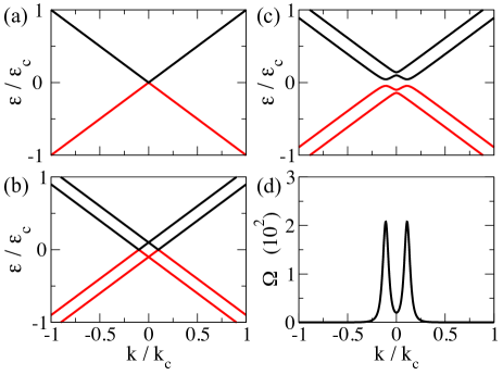
Fig. 1 illustrates the evolution of the electronic structure as the exchange field and Rashba SO coupling are introduced to the system. As shown in Fig. 1(b), the exchange field splits the original spin-degenerate Dirac cone into two oppositely spin-polarized copies, and this in turn produces spin degeneracy circles in momentum space at energy . Introducing the SO coupling causes a gap to open up between the conduction and valence bands around this circle along which SO coupling mixes up and down spins and produces an avoided band crossing. The momentum magnitude at which the avoided crossing occurs and the gap are given by
| (8) |
In the insulating regime when the Fermi level lies within the bulk gap, the Hall conductivity where is the Chern number which can be evaluated using the Thouless-Kohmoto-Nightingale-den Nijs (TKNN’s) formula BerryPhaseRMP :
| (9) |
where labels the bands below the Fermi level, and is the Berry curvature
| (10) |
with denoting the Bloch state for band . Before calculating the Chern number, we briefly comment on and make connections with two other formulas in the literature that are also used to calculate the Hall conductivity in the insulating regime.
For two-band Hamiltonians that can be written in the form , the TKNN formula can be written in the form
| (11) |
where is the unit vector which specifies the direction of . The right hand side of Eq. (11) can be identified as a Pontryagin index which is equal to the number of times the unit sphere of spinor directions is covered upon integrating over the Brillouin zone. For the present case, however, the graphene Hamiltonian contains both spin and pseudospin degrees of freedom, and Eq. (11) is not applicable. In this case, is given by the following more general form of the Pontryagin index Volovik :
| (12) |
where , is the anti-symmetric tensor, and is the Green function. In the non-interacting limit we consider in this work, Eq. (12) can be shown to be equivalent Yakovenko to the TKNN formula Eq. (9).
We now evaluate the component of the Berry curvature from Eq. (10) for the bands which are labeled by and . For each valley, we find that the Berry curvature is analytically expressible in terms of an exact differential
| (13) |
and the Chern number per valley for each band is given by
| (14) |
The upper limits of the integrand in Eq. (14) can be set to because the Berry curvature is large only close to valley centers.
Computing Eq. (14), we find that in this continuum model the Chern number for the individual valence band with is not quantized but instead depends numerically on the specific values of and . We find, however, that the two contributions always sum to and therefore each valley carries a unit Chern number. Taking into account both valleys, it follows that the quantized Hall conductivity is
| (15) |
III III. Gated Bilayer Graphene
We extend our discussion to the case of bilayer graphene. In the vicinity of valley K, we can write the bilayer graphene Hamiltonian in the presence of Rashba SO coupling , exchange field and potential imbalance as ( denotes Pauli matrices for the layer degrees of freedom):
| (16) | |||||
where is the interlayer hopping energy Mccann . For the other valley K’, the Hamiltonian is given by the above with . For generality, we have written Eq. (16) allowing for different Rashba SO coupling strengths and for the top and bottom layers. We shall now set for simplicity as the specific values of on the two layers do not alter the topology of the bands in our discussions below.
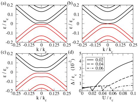
The Hamiltonian Eq. (16) is not diagonalizable analytically Remark . We therefore obtain the eigenenergies and eigenvectors numerically and use these to compute the Berry curvature. Fig. 2 shows the band structure evolution for increasing values of : (panel a), (panel b), and (panel c). For , an inverted-gap profile appears that is similar to the single-layer graphene case (Fig. 1c). At , the gap closes exactly at , and reopens when . Fig. 2 shows the behavior of the gap as a function of the potential difference for various values of . We find that initially increases with and then decreases toward zero when approaches the value of , after which increases again with .
The Berry curvature Eq. (10) can be expressed in a form that is more convenient for numerical computation. For the band, the Berry curvature per valley can be expressed as
| (17) |
where . Numerically diagonalizing the Hamiltonian Eq. (16) and computing the Chern number we find that
| (18) |
For , the Chern number is twice that of the single-layer graphene case, corresponding to four edge modes. The bilayer graphene system behaves as an quantum anomalous Hall insulator when , and exhibits vanishing Hall effect when . The gated bilayer graphene system therefore has a Hall current which is tunable by an external gate voltage.
The potential difference breaks the bilayer’s top-bottom spatial inversion symmetry. This produces a valley Hall effect in which valley-resolved electrons scatter to opposite sides of the sample. This can be characterized by the valley Hall conductivity which is defined as the difference between the valley-resolved Hall conductivities . We find that
| (19) |
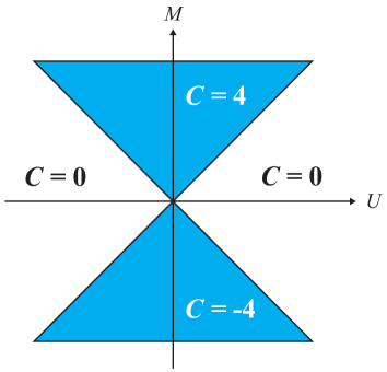
Therefore, despite having a vanishing Chern number when , the system exhibits a finite valley Hall conductivity . The quantum anomalous Hall and quantum valley Hall effects thus occupy complementary regions in the phase space, as summarized in the phase diagram Fig. 3. The gated bilayer graphene system therefore behaves, depending on whether or is larger, either as a quantum anomalous Hall insulator or a quantum valley Hall insulator.
IV IV. Edge State Properties
We have presented an analysis of bulk topological properties in single-layer and bilayer graphene cases using the low-energy Dirac Hamiltonian. In this section, we study the corresponding edge state properties on a finite single-layer and bilayer graphene sheet, and switch to a tight-binding representation from which we obtain the edge bands numerically. The finite-size single-layer and bilayer graphene sheets in our calculations are terminated with zigzag edges along one direction, and are infinite in the other direction. The Hamiltonian for single-layer graphene case can be expressed as
| (20) | |||||
where the first term describes hopping between nearest-neighbors on the honeycomb lattice, the second term is the Rashba SO term with coupling strength ( is a unit vector pointing from site to site ), and the third term is the exchange field . denote spin indices.
The bilayer graphene case is described by the Hamiltonian
| (21) | |||||
where are the top (T) and bottom (B) layer Hamiltonians of Eq. (20), vertical hopping between the layers is represented by the third term and occurs only between Bernal stacked neighbors, and the last two terms describe the potential difference applied across the bilayer. The parameters in the tight-binding Hamiltonians Eqs. (20)-(21) above are related to those in the low-energy Hamiltonians Eq. (1) and Eq. (16) as ( is the graphene lattice constant), , and are the same in both equations.
IV.1 Single-layer graphene case
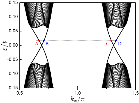
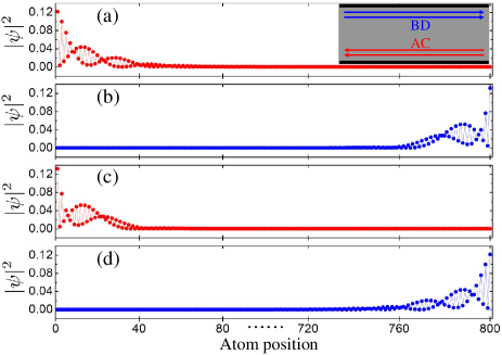
Fig.4 shows the ribbon band structures calculated from Eq. (20). Inside the bulk gap, we find counter propogating gapless edge channels at each valley that are localized on opposite edges of the graphene sheet. In the Fig.5, we plot the probability density profile of edge state wave functions as a function of the atom positions along the width of the graphene sheet for the four edge states labeled by A, B, C, D in Fig.4. It can be seen that states A and C are localized along the left edge whereas B and D are localized along the right edge. The edge states labeled by A and C have the same velocity and propagate along the same direction along one edge [inset of Fig.5(a)], whereas B and D have opposite velocity and propagate along the other edge. The two chiral edge modes each carry a unit conductance yielding a quantized Hall conductivity . In the appendix we also present an envelope function analysis of the edge state properties. The edge state band structure obtained with this approach is found to be in excellent agreement with the tight-binding results.
IV.2 Gated bilayer graphene case
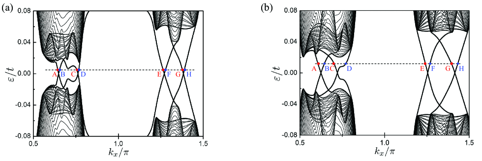
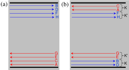
To study the edge state properties corresponding to the quantum anomalous Hall phase and the quantum valley Hall phase, we show the edge state band structure at a fixed Rashba SO coupling for the two cases and in Fig. 6. In contrast to the band structure in the single layer case Fig. 4, we find that the bilayer graphene band structure becomes asymmetric at K and K’. Within the bulk gap, there exists two edge bands associated with each valley. In Fig. 7 we show the probability density of the edge state wave function for the edge states labeled from A to H in Fig. 6 for both cases. The left panel shows the case , and we find that the edge states labeled by A, C, E, G are localized on one edge whereas B, D, F, H are localized on the other edge. This corresponds to the quantum anomalous Hall phase [Fig. 8(a)], where there exists four parallel chiral edge modes yielding a quantized Hall conductance .
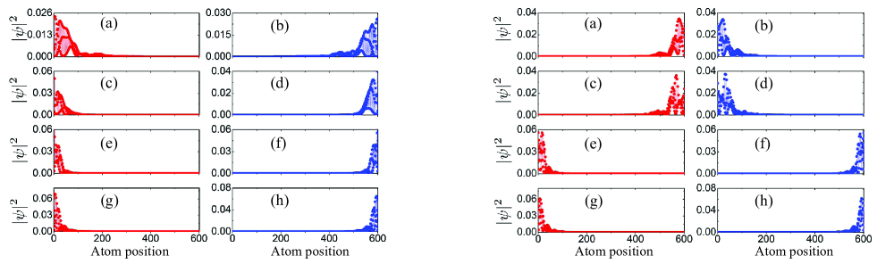
For the case , the right panel of the wave function plot Fig. 7 reveals that the four edge modes A, C, E, G which propagate along the same direction now become split between the two edges: A and C travel along one edge whereas E and G travel along the opposite edge. Similarly, for the edge modes that travel in the opposite direction, B and D propagate along one edge whereas E and G propagate along the other edge. This is illustrated in the schematic of Fig.8(b). Since the total current along one edge now adds up to zero, the Hall conductivity vanishes. Nevertheless, two sets of counter-propagating edge modes that belong to different valleys K and K’ travel along one edge. This situation bears a remarkable resemblance to the quantum spin Hall effect where one edge consists of two counter-propagating spin polarized modes. Due to the broken top-bottom layer spatial inversion symmetry, bilayer graphene exhibits a quantized valley Hall effect, with . In the case of single-layer graphene, such a quantized valley Hall effect arises when the A-B sublattice symmetry is broken; however there is no obvious strategy for imposing such an external potential experimentally. Through top and back gating, bilayer graphene allows for a more experimentally accessible way to produce the quantum valley Hall effect. Our present results show that the quantum valley Hall effect can coexist with time reversal symmetry breaking, provided that the breaking of spatial inversion symmetry wins over that of time reversal symmetry.
V IV. Conclusion
In summary, we have studied the quantum anomalous Hall effect in single-layer and bilayer graphene systems with strong Rashba spin-orbit interactions due to externally controlled inversion symmetry breaking, and strong exchange fields due to proximity coupling to a ferromagnet. For neutral single-layer graphene, we find that the Hall conductivity is quantized as . For bilayer graphene, in which an external gate voltage can introduce an inversion symmetry breaking gap, we find a quantized Hall conductivity at neutrality equal to when the potential difference is smaller than the exchange coupling . This anomalous Hall effect is similar to the quantized anomalous Hall effect sahetheory ; saheexpt which can occur spontaneously in high-quality bilayers at low-temperatures, but is potentially more robust because it relies on external exchange and spin-orbit fields rather than spontaneously broken symmetries. When , the system exhibits a quantized valley Hall effect with valley Hall conductivity .
Two obstacles stand in the way of realizing the quantum anomalous Hall effects discussed in this paper experimentally. It will be necessary first of all to introduce a sizeable Rashba spin-orbit coupling. One possibility is surface deposition of heavy-nucleus magnetic atoms that induce large spin-orbit coupling. The exchange field that is also required could be introduced through a proximity effect. From our ab initio studies TBpaper , an exchange field splitting of and Rashba spin-orbit coupling can be obtained by depositing Fe atoms on the graphene surface. Another possible solution is to deposit graphene on a ferromagnetic insulating substrate. The presence of a substrate breaks spatial inversion symmetry, and therefore also produces Rashba spin-orbit coupling. Since the exchange field is induced through a proximity effect, layered antiferromagnetic insulators, which are more abundant in nature can also be used and offer the advantage of an enlarged pool of candidate substrate materials.
VI Acknowledgement
This work was supported by the Welch grant F1473 and by DOE grant (DE-FG03-02ER45958, Division of Materials Sciences and Engineering). Y.Y. was supported by NSFC (No. 10974231) and the MOST Project of China (2007CB925000, 2011CBA00100).
VII Appendix: Envelope function analysis of edge modes
In this appendix, we present results for the edge state band structures using an envelope function approach based on the continuum Dirac model. We shall present only the single-layer graphene case below, as the bilayer case does not offer as much analytic tractibility since the Hamiltonian Eq. (16) is not analytically diagonalizable. We first calculate the envelope-function band structure and then compare the results with the tight-binding band structure.
Consider below a graphene sheet of infinite extent in the direction but finite in the y direction spanning from to . From the Hamiltonian Eq. (1), one can write down the eigenvalue problem satisfied by the wavefunction
| (26) | |||
| (27) |
For zigzag-edged graphene, the following boundary conditions apply
| (28) | |||||
| (29) |
The solution of the problem Eq. (27) admits the ansatz . Substituting into Eq. (27), we obtain the energy dispersion in terms of from the resulting determinantal equation
| (30) | |||||
which in turn yields four characteristic lengths in terms of the energy :
| (31) |
Note that in general can be complex, corresponding to a mixture of the edge and bulk states. The eigenvectors can be obtained as
| (32) |
where we have left out an inessential normalization constant. The total wavefunction can therefore be represented as a linear superposition of the constituent basis wavefunctions
| (33) | |||||
Using the boundary conditions Eqs. (28)-(29), we obtain the following determinantal equation
| (34) |
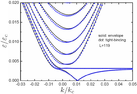
where . With given by Eq. (31), the band structure as a function of can be obtained from solving Eq. (34). We illustrate in Fig. 9 the resulting band structure in the vicinity of a Brillouin zone corner, from which it can be seen that both the bulk and edge bands obtained from the envelope function approach show excellent agreement with the tight-binding result.
*On leave from University of Texas at Austin.
References
- (1) A. H. Castro Neto, F. Guinea, N. M. R. Peres, K. S. Novoselov, and A. K. Geim, Rev. Mod. Phys. 81, 109 (2009).
- (2) I. Zutic, J. Fabian, and S. Das Sarma, Rev. Mod. Phys. 76, 323 (2004).
- (3) C. L. Kane and E. J. Mele, Phys. Rev. Lett. 95, 146802 (2005).
- (4) H. Min, J. E. Hill, N. A. Sinitsyn, B. R. Sahu, L. Kleinman, and A. H. MacDonald, Phys. Rev. B 74, 165310 (2006).
- (5) Y. G. Yao, F. Ye, X.-L. Qi, S.-C. Zhang, and Z. Fang, Phys. Rev. B 75, 041401(R) (2007).
- (6) M. Gmitra, S. Konschuh, C. Ertler, C. Ambrosch-Draxl, and J. Fabian, Phys. Rev. B 80, 235431 (2009).
- (7) E. I. Rashba, Sov. Phys. Solid State 2, 1109 (1960).
- (8) A. Varykhalov, J. Sánchez-Barriga, A. M. Shikin, C. Biswas, E. Vescovo, A. Rybkin, D. Marchenko, and O. Rader, Phys. Rev. Lett. 101, 157601 (2008).
- (9) O. Rader, A. Varykhalov, J. Sánchez-Barriga, D. Marchenko, A. Rybkin, and A. M. Shikin, Phys. Rev. Lett. 102, 057602 (2009).
- (10) Z. Qiao, S. A. Yang, W. Feng, W.-K. Tse, J. Ding, Y. G. Yao, J. Wang, and Q. Niu, Phys. Rev. B 82, 161414(R) (2010).
- (11) F.D.M. Haldane, Phys. Rev. Lett. 61, 2015 (1988).
- (12) M. Onoda and N. Nagaosa, Phys. Rev. Lett. 90, 206601 (2003).
- (13) C. X. Liu, X.-L. Qi, X. Dai, Z. Fang, and S.-C. Zhang, Phys. Rev. Lett. 101, 146802 (2008).
- (14) R. Yu, W. Zhang, H.-J. Zhang, S.-C. Zhang, X. Dai, and Z. Fang, Science 329, 61 (2010).
- (15) C. Wu, Phys. Rev. Lett. 101, 186807 (2008).
- (16) M. Zhang, H. Hung, C. Zhang, and C. Wu, arXiv:1009.2133v2 (2011).
- (17) E. I. Rashba, Phys. Rev. B 79, 161409(R) (2009).
- (18) M. Zarea and N. Sandler, Phys. Rev. B 79, 165442 (2009).
- (19) R. van Gelderen and C. Morais Smith, Phys. Rev. B 81, 125435 (2010).
- (20) R. Winkler and U. Zulicke, Phys. Rev. B 82, 245313 (2010).
- (21) D. J. Thouless, M. Kohmoto, M. P. Nightingale, and M. den Nijs, Phys. Rev. Lett. 49, 405 (1982); D. Xiao, M.-C. Chang, and Q. Niu, Rev. Mod. Phys. 82, 1959 (2010).
- (22) G. E. Volovik, The Universe in a Helium Droplet (Oxford, 2003).
- (23) K. Sengupta and V. M. Yakovenko, Phys. Rev. B 62, 4586 (2000).
- (24) E. McCann and V. I. Fal’ko, Phys. Rev. Lett. 96 086805 (2006).
- (25) One is tempted to arrive at a low-energy Hamiltonian from the Hamiltonian Eq. (16) by treating the tunneling perturbatively as in Ref. Mccann . Such a Hamiltonian however would not predict the correct quantized anomalous Hall or valley Hall conductivity, because the higher-energy bands also contribute to the Hall response.
- (26) H. Min, G. Borghi, M. Polini, and A. H. MacDonald, Phys. Rev. B 77, 041407(R) (2008); F. Zhang, H. Min, M. Polini, and A. H. MacDonald, Phys. Rev. B 81, 041402(R) (2010); R. Nandkishore and L. Levitov, Phys. Rev. B 82, 115124 (2010).
- (27) J. Martin, B. E. Feldman, R. T. Weitz, M. T. Allen, A. Yacoby, arXiv:1009.2069 (2010); R.T. Weitz, M. T. Allen, B. E. Feldman, J. Martin, and A. Yacoby, Science 330, 812 (2010).