Modeling Rectification Effects in Mesoscopic Superconducting Devices
Abstract
We study thermal fluctuations and capacitive effects on small Josephson Junction Rings (JJR) that mimics the rectification phenomena recently observed in triangle shaped mesoscopic superconductors, due to the superposition of the field induced persistent current with the bias current. At finite temperature we predicted that the amplitude of the rectified signal depends strongly on the current contacts configuration on the JJR, in coincidence with experiments. In addition we analize the range of parameters where a closed loop of capacitive junctions is an appropriate model to explain the experimental observations. We conclude that the closed loop of weak links, a JJR, is a simple, robust and good enough model to explain the observed voltage rectification effects on mesoscopic superconducting samples for a wide range of temperature.
keywords:
ratchet effect , mesoscopic superconducting devices , Josephson junction arrays1 INTRODUCTION
Technological progress allowing the manipulation of ratchet effects in complex systems such as cold atoms [1], colloids [2], cells [3], fluids [4], electrons in semiconductors [5], extended magnetic walls [6], vortices in Josephson systems [7, 8], motivate this work. In all the mentioned examples the flux of driven particles interact with an asymmetric potential. The key question on this field is that it is not simple in each case to know feasibly which are the mechanisms underlying these many bodies rectification effects. It is well known that the velocity of a single overdamped particle under an applied ac force can be rectified by introducing a periodic potential with broken reflection symmetry [9]. We can thus ask whether this effect, known as rocking ratchet (because the system is rocked with an external ac force), can be still observed as a rectified dc voltage response in transport measurements in singly connected mesoscopic superconductors under external ac bias currents, thermal fluctuations and external homogenous magnetic field applied. Indeed finite dc voltage was measured under zero averaged ac current applied and it was extensively studied in superconducting (SC) nanostructures [10, 11, 12]. But this system differs from examples mentioned previously, because the essential broken symmetry required to obtain a rectifier is controlled differently in these samples, it is controlled by its geometry (sample shape) and the configuration of contacts leads (position of the current/voltage probes). In particular, motivated by these recent experiments reporting original voltage rectification effects in mesoscopic superconducting triangles [11] we simulated a more realistic model for such system in order to understand and corroborated the physics behind the observed ratchet effects, with special emphasis in the finite temperature effects not taking into account in previous and simpler models.
In a pionner analytical work [13] different asymmetric type-II superconducting structures (rings and strips) were already proposed and analyzed under current and magnetic field applied. They show how magnetic flux penetration depending on the geometric parameters is fieldlike or currentlike. Later on, measurements were realized in asymmetric SC rings [14, 15]. In addition similar rectification effects were reported in a singly connected structured if the current injection is off-center [10]. From mentioned works it is widely accepted that the effects observed are due to the asymmetry causing a difference in critical current for a positive or negative applied external current which is compensated or reinforced by the field induced persistent current. Further an important parameter, temperature, should be taking into account to model in detail the phenomena observed. First because all results reported in single triangle samples are done close to [10, 11, 12], it means where thermal fluctuations are important and far away from where previous theoretical analysis was done [11]. In addition it is well known that geometry in microsized or in nanosized samples could play essential roles in fluctuations phenomena and even more, very recently it was shown that the superconducting order parameter present larger thermal fluctuations in the corners of sharp shaped samples [16]. At present, when smaller dimensions are manipulated it is motivating to study effects of thermal fluctuations even at temperature much lower than where dimensionality start to compete and the limits between thermal fluctuations and quantum fluctuations are not clear. In short, to understand how thermal fluctuations influence the rectification phenomena at all finite temperature is important.
In this paper we model voltage rectification effects observed in thin mesoscopic superconducting triangles [11] using two kind of small Josephson Junction Rings: a resistive one, using the RSJ (resistively shunted junction) model and a capacitive model, using the RCSJ (resistevely and capacitive shunted junction) model. We introduce finite temperature effects adding white noise to the resulting dynamics equations within the RSJ model. We find good qualitative agreement with experiments.
2 SIMULATED MODEL
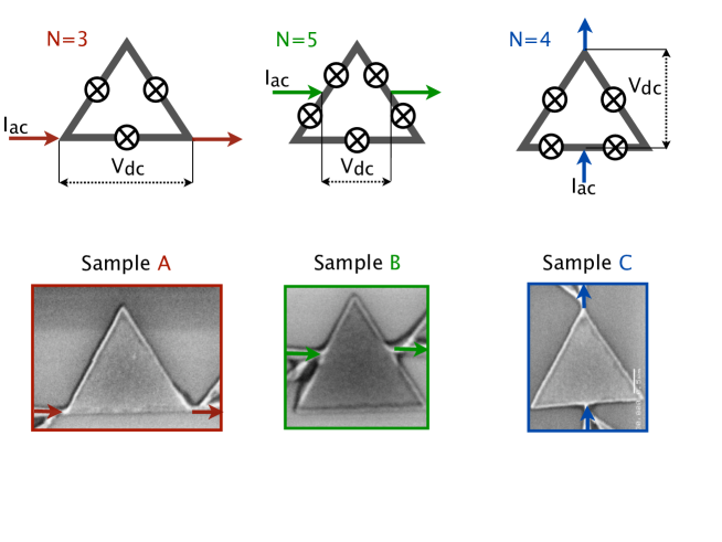
We study at finite temperature the dynamics of small Josephson Junction Rings (closed loops) with a finite number of identical Josephson junctions (JJ): three JJ , four JJ or five JJ, as sketched in Fig.1 for different positions of the current injection. An external sinusoidal ac current is applied in different loop points as shown in Fig.1 in order to mimics the different contact configurations, samples A, B and C used in experiments [11].
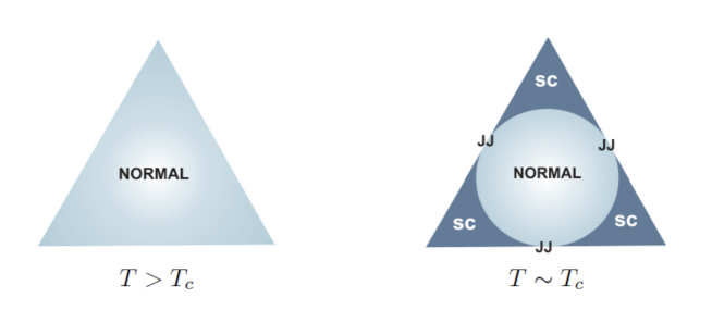
In Fig.2 we show a schema of the shape in which superconductivity nucleation occurs in triangle shaped mesoscopic samples. It is well known that nucleation in mesoscopic samples is dominated by the surface superconductivity and its shape and boundaries, i.e by its geometry. In fact, it was clearly shown that surface nucleation is enhanced in wedge shaped superconductors [17, 18], then the idea to model the triangle as a loop of strong superconducting electrodes (SC islands) at the triangle corners connected by weak links is reasonable. Those weak links, could be an insulator as Josephson proposed originally (SIS JJ) or a normal metal (SNS JJ), or simpler a short narrow constriction of the same superconductor (ScS JJ) [20]. Our main assumption for the calculations is that the superconducting order parameter is such that with the same constant on all SC islands and is spatially constant in each island. Then our variables will be the superconducting phases in each SC island.
We started solving the simpler case, the ring of weak links of SNS junctions, using the resistively shunted junction (RSJ) model plus thermal fluctuations and solving numerically the superconducting phase dynamics using Langevin dynamics technique [19]. We considere a total magnetic field applied perpendicular to the ring, spatially and temporally constant. The Hamiltonian of a closed loop of SNS-junctions is the following:
| (1) |
where is the Josephson energy, is the superconducting phase difference at the junction , and is the phase of the superconducting island centered at
| (2) |
being the ring radius. Note here that our loops imitating the triangle samples, are ideal junction circles where the needed triangle asymmetry can be introduce controlling the number of junctions and the points where external currents are injected and extracted (see Fig. 1). The total magnetic field is . The magnetic field contribution to the phase difference is the line integral of the vector potential between sites and ,
| (3) |
being the single superconducting quantum flux. After taking the magnetic field applied perpendicular to the sample plane, , the invariant gauge for the vector potential and the flux quantum number through the ring we obtain after solving the corresponding previous integral in polar coordinates:
| (4) |
The current flowing in the JJ between two superconducting islands is modeled by a typical electric circuit build up of an ideal JJ in parallel with a normal resistance, i.e by the sum of the Josephson supercurrent and the normal electron current. Conservation of current is considered with Kirchhoff laws fulfilled in each node. We inject a current between junctions and , and extract it junctions away, between junctions and . The resulting set of dimensionless equations for the currents flowing in the ring is the following:
| (5) |
| (6) |
| (7) |
which are first order differential equations for the time evolution of the phase variables . is the current flowing in the upper branch of the ring, up with respect to the injection and extraction current points, and . Let us note that each junction interacts with all the others through , the total current in the upper branch of the circuit, which represents a kind of mean-field interaction plus a drive. In addition finite temperature effects are taking into account through an added Langevin noise term , introduced as current fluctuations, which models the contact with a thermal bath at temperature and satisfies the condition for non-correlated white noise:
| (8) |
where is the normal state resistance. In short the model control parameters are the external current , magnetic field applied or magnetic flux and temperature T. In addition one can play with the source-drain distance and the number of junctions N.
Langevin dynamical equations Eq. 5-6 using conditions (4) and (7) are solved numerically using a second order Runge-Kutta-Helfand-Greenside algorithm under an external sinusoidal current applied . We calculate the mean voltage response computing the instantaneous dc voltage drop between source and drain:
| (9) |
In fact there is a second equivalent form to compute the voltage drop, if upper and lower paths contain a different number of junctions:
| (10) |
We normalize currents by the single junction critical current , voltages by , temperature by and the unit of time is =.
Possibly weak links sketched in Fig. 2 could be more complex than the simpler SNS junctions, like tunnel superconducting-insulator-superconducting (SIS) junctions and a more complete description is required. Then we probe if the essential features of previous experiments [10, 11] are as well described by a RCSJ (resistively and capacitively shunted junction, [20]) ring. In this model the weak link (JJ) is modeled by an ideal JJ shunted in parallel by a resistance and a capacitance . The addition of capacitive effects accounts for the geometric shunting capacitance between the two superconducting islands. Now the following set of second order differential equations should be solved:
| (11) |
| (12) |
being the main parameter now, a measurement of the system dissipation, and is known as the McCumber parameter [21], or damping parameter equal to with the plasma frequency of the junction .
3 RESULTS
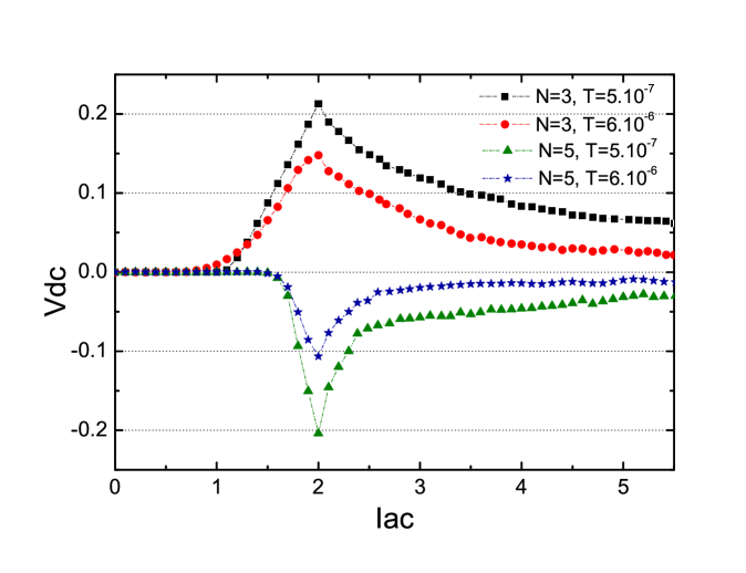
In order to study the influence of contacts on the rectification effects observed in superconducting triangles [11] the model for RSJ rings described in previous section was first solved numerically. We calculated the rectified mean dc voltage as a function of the ac current amplitude, , in the low frequency limit at finite temperatures and for different magnetic fields applied perpendicularly to the samples. The results for closed loops with junctions (which mimics the experimental contacts configuration of sample A) and (sample B), both with the same source-drain distance , are shown in Fig. 3.
We can clearly see that at finite temperature both, the and devices display finite rectified voltage, above a critical current. Examples for a fixed magnetic field corresponding to , i.e. for and two temperature values are shown. The junction loop with presents a clear difference comparing with the case , the rectified voltage is inverted, , resulting both junction loops in good choices to reproduce the experimental results obtained in Ref. [11] for both type of asymmetric contact configurations, sample A and sample B, for which inverted rectified voltage responses were reported. In short, this simple model including thermal fluctuations mimics correctly recent experimental results [11]. Other details could be extracted from Fig. 3, all examples shown present a critical current amplitude threshold that decreases with temperature and it is larger for the device with the larger number of junctions, . We can also conclude that the maximum of is almost the same in both cases when the temperature is closer to zero, but when temperature is increased these maximum decrease, as it is expected when thermal fluctuations are present, but the rates are different depending on the sample type, the maximum rectified voltage decreases quicker in the larger loop, . At both cases present a maximum at but when temperature is decreased more than an order of magnitude, , the maximum is for and for . In addition decays to zero with , as expected, but this behavior is quicker for .
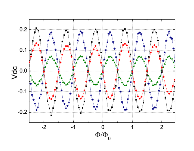
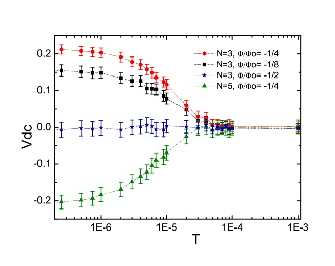
Another interesting feature to analize is the voltage response related to the total magnetic field applied, . An important behavior is obtained and analyzed in Fig.4, where qualitatively the same oscillations for as a function of vorticity (magnetic flux through the ring) are also obtained in the experiments [11]. Three characteristics of the oscillations dependency on magnetic field are found to be independent of temperature: (a) the rectification effects disappear if , being an integer, (b) the maximum absolute value of the rectified voltage appears always the condition is fulfilled and (c) if . The observed dependences of rectified voltage on magnetic field are in accordance with expected Little-Parks oscillations, which occur every time the vorticity of the system increase due to the entrance of a new vortex: [22]. In addition a noticeable feature appears, the sign of the rectified voltage changes, from negative if to positive if (being an integer) for and signs are inverted for . This opposite behavior between both devices is related with its asymmetry and it is the best evidence that indeed the observed rectification effects are due to the superposition of the external applied sinusoidal current (bias current) with the field induced persistent current circulating around the JJRs. The external current injection is well below the geometrical center for device on the contrary to device, then an opposite current compensation behavior was obtained. It is worth to mention that all simulations were performed as well for the symmetric current injection case, sample C, and no voltage response was observed, corroborating the essential need of an off-center current injection (system asymmetry induced externally for the contacts configuration). Note that decreases to zero while temperature is increased, in both cases. In order to analyze this last feature in detail comparing both contact configurations, the rectified dc voltage as a function of temperature is shown in Fig. 5 for and some typical values of the magnetic field applied, corresponding to (maximum voltage response), (intermediate voltage response) and (minimum voltage response). For fields with finite response, the absolute value of the rectified voltage decrease smoothly to zero with similar temperature functionality while temperature is incremented slowly in several orders of magnitude. It is worth to mention that it remains finite for a wide range of temperature. Analyzing the three curves presented for , a rectified voltage tendency to zero as the magnetic flux approach to is observed as well, in coincidence with previous Fig. 4. These results show clearly the robustness of the rectification effects under a wide range of thermal fluctuations for all magnetic field applied such that .
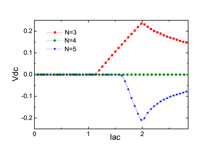
In short we found that simple loop of weak links modeled with a resistive shunted model () plus thermal fluctuations is in good agreement with experimental results. The following question naturally arises: is a ring of capacitive Josephson junctions, i.e. a capacitive and resistive shunted model () a suitable model to explain the observed phenomena?. In order to get an insight into this point we include the capacitive effects in our simulations. As an illustration in Fig.6 a comparison of the mean dc voltage response vs among the three type of contact configurations () is shown. The results presented were obtained at zero temperature for a magnetic flux . A capacitive model without thermal fluctuations is shown to be a good aproximation to the experimental observations if . In Fig. 6 one -value is shown for clarity, , but simulations were performed incrementing till unity, and similar results were obtained regarding our previous main conclusions in comparison with experimental results observed in Ref. [11].
4 CONCLUSIONS
In summary, at finite temperature we predicted within a model system that the amplitude of the rectified signal depends strongly on the current contacts configuration in the JJR, in good agreement with recent diode effects measured in Al mesoscopic triangles [10, 11] and in coincidence as well with a more sophisticated model including capacitive effects. Our results corroborate that the clue behind the observed rectification effects in triangle shaped SC is indeed the superposition of the field induced persistent current with the bias current, being these phenomena robust and strong enough in front of thermal fluctuations and for more complicated modeling of the weak links. The key ingredients to observe the dc voltage rectification described here under thermal fluctuations are indeed field induced persistent currents and asymmetry induced by an off-center injection of external currents. This recipe suggests that similar rectification effects, strongly robust under finite temperature, should be also present in every system with a persistent current and an asymmetric current path, being useful to design and control newer and smaller diode devices.
5 Acknowledgment
This work was supported by CONICET (PIP 112-200801-01576; 00965/10), SeCyT-UNCórdoba and ANPCyT (PICTO66/2008), Argentina. The authors specially acknowledge A.V. Silhanek for useful suggestions and experimental images shown in Fig. 1 and A.B. Kolton for useful discussions.
References
- [1] R. Gommers, S. Denisov, and F. Renzoni, Phys. Rev. Lett. 96, 240604 (2006).
- [2] A. Libál, C. Reichhardt, B. Jankó, and C. J. O. Reichhardt, Phys. Rev. Lett. 96, 188301 (2006).
- [3] G. Mahmud, C. J. Campbell, K. J. M. Bishop, Y. A. Komarova, O. Chaga, S. Soh, S. Huda, K. Kandere-Grzybowska, and B. A. Grzybowski, Nature Physics 5, 606 (2009).
- [4] S. Matthias and F. Muller, Nature 424, 53 (2003).
- [5] H. Linke et al., T. Humphrey, A. Lofgren, A. Sushkov, R. Newbury, R. Taylor, and P. Omling, Science 286, 2314 (2003).
- [6] A. Pérez-Junquera, V.I. Marconi, A.B. Kolton, L.M. Alvarez-Prado, Y. Souche, A. Alija, M. Vélez, J. V. Anguita, J.M. Alameda, J.I. Martín, and J.M.R. Parrondo, Phys. Rev. Lett. 100, 037203 (2008).
- [7] F. Falo, P. J. Martínez, J. J. Mazo and S. Cilla, Europhys. Lett. 45, 700 (1999); E. Trías, J. J. Mazo, F. Falo, and T. P. Orlando, Phys. Rev. E. 61, 2257 (2000).
- [8] D. E. Shalóm and H. Pastoriza, Phys. Rev. Lett. 94, 177001 (2005); V. I. Marconi, Phys. Rev. Lett. 98, 047006 (2007).
- [9] Peter Reimann, Physics Reports 361 57 265, (2002).
- [10] M. Morelle, N. Schildermans, and V. V. Moshchalkov, Appl. Phys. Lett. 89, 112512 (2006).
- [11] N. Schildermans, A. B. Kolton, R. Salenbien, V. I. Marconi, A. V. Silhanek and V. V. Moshchalkov, Phys. Rev. B. 76, 224501 (2007).
- [12] Nele Schildermans PhD Thesis “Rectification effects and nucleation superconductivity in superconducting nanostructures”, KULeuven, Belgium, October 2008.
- [13] E. H. Brandt and M. Indenbom, Phys. Rev. B. 48, 12893 (1993).
- [14] S. V. Dubonos, V. I. Kuznetsov, I. N. Zhilyaev, A. V. Nikulov, and A. A. Firsov, JETP Lett. 77, 371, 2003.
- [15] V. L. Gurtovoi, S. V. Dubonos, A. V. Nikulov, N. N. Osipov and V. A. Tulin. Preprint cond-mat: arXiv:0903.3539v1, 20 Mar 2009.
- [16] W. V. Pogosov, V. R. Misko and F.M Peeters. Preprint cond-mat: arXiv:1009.0590v1, 3 Sep 2010.
- [17] V. M. Fomin, V. R. Misko, J. T. Devreese, and V. V. Moshchalkov, Solid State Commun. 101, 303, 1997.
- [18] V. A. Schweigert and F. M. Peeters, Phys. Rev. B, 60, 3084 1999.
- [19] J. S. Chung et al., Phys.Rev.B 40, 6570 (1989); D. Domínguez, Phys. Rev. Lett. 72, 3096 (1994); V.I. Marconi et al., Phys. Rev. Lett. 82, 4922 (1999);ibid. 87, 0170004 (2001); V. I. Marconi et al., Phys. Rev. B. 63, 174509 (2001).
- [20] M. Tinkham, Introduction to Superconductivity, Second Edition Dover Publications, INC. N.York (1996).
- [21] D. E. McCumber, J. Appl. Phys. 39, 3113 (1968).
- [22] W. A. Little and R. D. Parks, Phys. Rev. Lett. 9, 9 (1962).