Controlled coupling of a single nitrogen-vacancy center to a silver nanowire
Abstract
We report on the controlled coupling of a single nitrogen-vacancy (NV) center to a surface plasmon mode propagating along a chemically grown silver nanowire. We locate and optically characterize a single NV-center in a uniform dielectric environment before we controllably position this emitter in the close proximity of the nanowire. We are thus able to control the coupling of this particular emitter to the nanowire and directly compare the photon emission properties before and after the coupling. The excitation of single plasmonic modes is witnessed and a total rate enhancement by a factor of up to 4.6 is demonstrated.
pacs:
73.20.Mf, 42.50.CtStrong enhancement of the fluorescence and scattered light from a single molecule, quantum dot, or nitrogen vacancy (NV) center can be observed by placing the particle in the vicinity of a metallic nano-sphere 2006Kuehn ; 2006Anger ; 2009Schietinger ; 1997Nie ; 1997Kneipp . This enhancement arises due to the excitation of strongly confined and localized surface plasmon on the metallic sphere. Despite the strong enhancement of emissive processes, the resulting photon emission in those realizations does not couple preferably to a dedicated spatial mode and are thus not directly suitable for applications in, for instance, quantum information processing where the coupling between a single spatial mode and a single emitter is often a requirement for scalability.
To obtain an efficient coupling to a specific spatial mode while exploiting the enhancement properties of strongly confined surface plasmons, it has been suggested to use propagating plasmons on cylindrical wires as opposed to localized plasmons 2006Chang . By using this method, it is possible to enhance the emissive process into one particular propagating plasmon mode which can be further transferred into a photonic mode of an optical waveguide with high efficiency 2008Pyayt ; 2009Chen . Such a light-matter interface mediated by surface plasmons can be used to efficiently generate single photons and to enable strong non-linearities at the single photon level which can be exploited to make a single photon transistor 2007Chang or to perform a near error-free deterministic Bell measurement 2010Witthaut .
The coupling of individual single photon emitters to propagating surface plasmon modes on individual silver nanowires has been demonstrated for CdSe quantum dots 2007Akimov and for NV-centers in nano-crystal diamonds 2009Kolesov . In these experiments, however, the wire-crystal systems were not deterministically assembled thus rendering the rate enhancement estimation highly uncertain. By comparing an ensemble of uncoupled single emitters with an ensemble of coupled single emitters, they estimated rate enhancement factors of 1.7 2007Akimov and 2.5 2009Kolesov .
In this letter, we demonstrate the controlled coupling of a single NV-center in a diamond nano-crystal to a surface plasmon mode propagating along a silver nanowire. The wire-crystal system is deterministically assembled by the use of an atomic force microscope. This approach allows us to directly compare the emission properties of a particular NV-center in a homogeneous dielectric environment with the emission properties of the same emitter but placed in the near vicinity of a silver nanowire supporting a propagating surface plasmon mode. The coupling to the propagating surface plasmon mode is evidenced by a decrease in the emitter lifetime and the emission of a single photon is verified by a measurement of the second-order correlation function.

Our experimental setup is a home-built inverted scanning confocal microscope using an oil immersion objective with a numerical aperture of 1.4 combined with a coaxially aligned atomic force microscope (AFM, NT-MDT SMENA), as illustrated in Fig. 1. For the excitation of NV-centers we either use a continuous wave or a pulsed laser, both operating at a vacuum wavelength of 532 nm. The pulsed laser has a repetition rate of 5.05 MHz and a pulse width of 4.6 ps. The fluorescence emission from the sample is collected by two optical channels and detected with avalanche photo diodes APD1 and APD2, respectively. The channel of APD1 is directly aligned with the pump beam, while the channel of APD2 is decoupled from the pump beam via a galvanometric mirror, as illustrated in Fig. 1. The fluorescence filters placed in front of both detectors are highly transmissive for photon wavelength between 647 nm and 785 nm. APD1 and APD2 compose, together with the beam splitter BS, the well known Hanbury-Brown and Twiss interferometer used for the characterization of a single photon source 1956HBT . The AFM can be operated in tapping mode or contact mode. Tapping mode operation is used to record the topography of the sample and with this to measure the height of the nanowire and the diamond crystals as well as the lateral position of individual nano-crystals with respect to the silver nanowire. By using the AFM in contact mode operation we are able to controllably push a chosen diamond nano-crystal across the sample. This technique is used to place a single diamond nano-crystal near a silver nanowire, thus controllably coupling the NV-center to the propagating plasmonic mode.
The sample was prepared on a plasma cleaned fused silica substrate. After the cleaning process, we first spin-coat nano-diamonds with sizes (MSY 0-0.05, Microdiamt AG) on the sample. Only a few of the nano-diamonds are optically active containing a single NV-defect. Chemically grown silver nanowires with diameters in the range and length of fabricated by a polyol reduction process of silver nitrate 2008Korte were subsequently spin-coated on the substrate resulting in a sufficient number of individual and well separated nanowires.
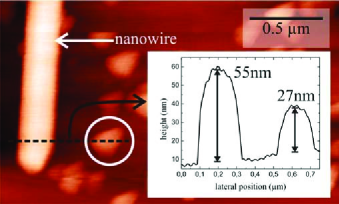
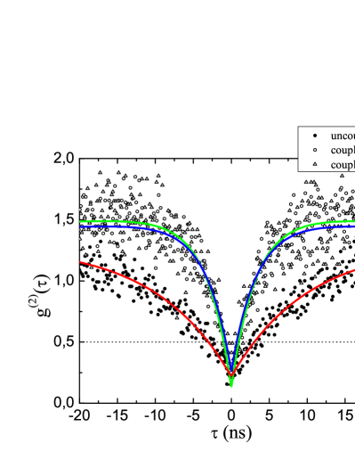
We started the experiment by recording a fluorescence image with APD1. The AFM topography image of the same area was then used to locate a suitable nano-diamond containing a single NV-defect. This diamond was separated from other diamonds and brought near the nanowire for characterizing the NV-center in a uniform dielectric environment. At this step of the experiment, the diamond was still well separated from the silver nanowire, as illustrated by the AFM-topography image shown in Fig. 2. In the inset of Fig. 2 we present the height profile of the silver nanowire and the diamond, which at maximum were measured to be nm and nm, respectively. The length of the nanowire was measured with the AFM to be about . With the diamond in this position, we measure the decay time of the NV-center’s excited state, which is shown by the black dots in Fig. 3. A single exponential fit yields an excited state lifetime of ns. In contrast to NV-centers in bulk diamond, where an excited state lifetime of is usually measured 1983Collins ; 2008Batalov , we attribute the increased lifetime to the decreased effective refractive index of the surroundings, which is significantly smaller than the refractive index of bulk diamond. The measured second order correlation function of this NV-center is presented by the black dots in Fig. 4 and the red line is a best fit to the data using the model of Ref. 2000Kurtsiefer . The emission of single photons is clearly confirmed by the fact that is well below . By measuring the fluorescence count rate as a function of the linear polarization of the pump beam, we verified that a large component of the NV-centers dipole moment is aligned perpendicular to the nanowire axis 2005Epstein ; 2009Schietinger .
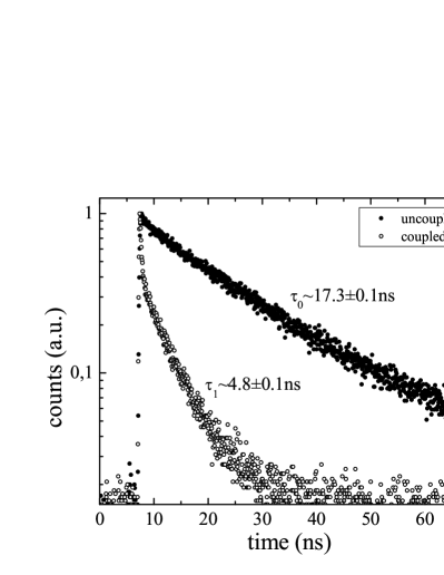
As a next step, we carefully push the nano-diamond in the very close proximity of the nanowire by operating the AFM in contact mode. The final position of the nano-diamond near the silver nanowire is indicated by the white arrow in the AFM topography image shown in Fig. 5 (a). The NV-centers dipole moment is still largely aligned perpendicular to the nanowire axis, which was verified by a new measurement of the count rate as a function of the linear polarization of the pump beam. As a consequence, the NV-center now feels a changed dielectric environment compared to its previous position. This is witnessed by the decrease of its excited state lifetime, as shown by the open circles in Fig. 3. Directly compared to the lifetime of the NV-center in its previous position, we measured a decrease of the excited states lifetime of the coupled system by a factor of Now, the NV-center does not only radiate to the far field, but also couples to the propagating plasmonic mode of the silver nanowire 2006Chang .
Evidence for the excitation of the propagating plasmonic mode is given by the fluorescence image recorded with the detector APD2, which is shown in Fig. 5 (b). This image has been obtained by continuously exciting the NV-center while scanning the image plane using the galvanometric mirror. Two emission spots can be seen in Fig. 5 (b). The emission spot labeled as ’A’ in Fig. 5 (b) comprises the radiative emission from the NV-center together with emission from the nearby nanowire end face. Spot ’B’ in Fig. 5 (b) only comprises emission from the far nanowire end face. The intensity measured from spot ’B’ is thus proportional to the coupling of the NV-center to the propagating plasmonic mode 2006Chang ; 2007Akimov ; 2009Kolesov . However, an exact estimation of the NV-center coupling to the propagating plasmonic mode by measuring the intensity of spot ’B’ is difficult due to plasmon propagation losses along the nanowire and the complex reflections at the nanowire end face in conjunction with the broad emission spectrum of the NV-center.

The function measurement with the detectors APD1 and APD2 being both aligned on emission spot ’A’ is shown by the open dots in Fig. 4. With the open triangles we present the function measurement between emission spot ’A’ and ’B’. The green and blue line represent a best fit to the data for both measurement realizations. In both cases, a confirms the generation of single photons, and the excitation of single propagating surface plasmon modes is confirmed by the measurement between spot ’A’ and ’B’.
Finally, we compare our experimental results with theoretical predictions 2006Chang . In Fig. 6 we plot the total rate enhancement for the relevant range of nanowire diameter and emitter distance from the nanowire surface. The calculation is done for a vacuum wavelength of and we use the Drude model to estimate the electric permittivity of silver 1972Johnsen . In order to account for the relatively high refractive index of diamond, the electric permittivity of the dielectric medium surrounding the nanowire was set to in the calculation. For the nanowire diameter of and a diamond height of we expect from these calculations a total rate enhancement of , assuming that the NV-center is located at the maximum position of away from the nanowire surface and that the NV-centers dipole moment is aligned parallel to the radial electric field component of the propagating plasmonic mode. This expected rate enhancement is in good agreement with our experimental result of . We emphasize that only for parallel alignment of the NV-centers dipole moment to , an efficient coupling to the propagating plasmonic mode is achieved, since for the relevant range of parameter where is the plasmon electric field along the nanowire axis.
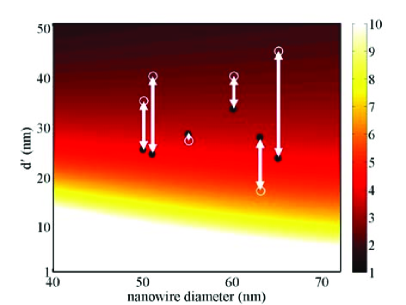
In TABLE 1 we summarize the relevant physical parameters for various NV-center/nanowire systems that we have successfully assembled. For all realizations we observe the excitation of a single surface plasmon, confirmed by . The coupling to the propagating plasmonic mode was witnessed by strong rate enhancement factors and verified by the observation of photon emission from the nanowire end face. In addition to the experimentally obtained rate enhancements we also present the minimum expected rate enhancement in column four of TABLE 1, calculated under the assumption that the NV-centers dipole moment is aligned parallel to . All measured and calculated enhancement factors are graphically illustrated in Fig. 6.
| nanowire | diamond | total rate | min. |
|---|---|---|---|
| diameter | height | enhancement | expected rate |
| (nm) | (nm) | enhancement | |
| 65 | 45 | 4.60.1 | 2.2 |
| 60 | 40 | 2.90.1 | 2.4 |
| 51 | 40 | 4.40.2 | 2.4 |
| 63 | 17 | 3.60.1 | 5.7 |
| 50 | 35 | 4.20.1 | 2.8 |
In view of improving the coupling efficiency of the NV-center to the plasmonic mode it is necessary to decrease both the diameter of the nanowire and the size of the diamond, as can be seen from Fig. 6. Thinner nanowires can, for instance, be obtained by an optimization of the nanowire fabrication process 2008Korte . As an alternative, it might also be possible to sculpture nanowires from chemically prepared metallic flakes using focused ion beam milling 2010Huang . The latter technique will have the advantage of gaining ultimate control over the nanowire dimensions. We have found experimentally, that nanowires made by electron beam lithography and thermal metal deposition are not suitable for coupling single NV-centers to their propagating plasmonic mode. Fluorescence from those nanowires largely overlaps with the emission spectrum of a NV-center, which as a direct consequence limits the possibility of detecting single photons. Surface roughness of lithographically prepared nanowires further limits the propagation distance of plasmonic modes 2005Ditlbacher . Nano-diamonds with sub-10 nm diameters containing single NV-centers with stable photon emission rates have recently been reported in the literature 2009Tisler ; 2010Bradac .
In conclusion, by the aid of an atomic force microscope we have nano-assembled a system comprising a single NV center in a nano-crystal diamond and a chemically grown silver nanowire. This method allowed us to directly compared the emission properties of a single NV-center in a uniform dielectric environment with the emission properties of the same emitter coupled to the nano-wire. An enhancement of the NV-centers decay rate by a factor of 4.6 is directly measured and the excitation of single surface plasmons is evidenced by the observation of single photon emission at the far end of the nanowire. We believe that the method presented in this article in combination with smaller diamonds and optimized metallic structures will pave the way for strongly coupled plasmonic systems.
We gratefully acknowledge fruitful discussions with Anders S. Sørensen and Fedor Jelezko. This project has been financially supported by the Villum Kann Rasmussen foundation, the Carlsberg foundation, and the Danish council for independent research - natural sciences (FNU).
References
- (1) S. Kühn, U. Håkanson, L. Rogobete, and V. Sandoghdar, Phys. Rev. Lett 97, 017402 (2006).
- (2) P. Anger, P. Bharadwaj, and L. Novotny, Phys. Rev. Lett. 96, 113002 (2006).
- (3) S. Schietinger et al., Nano Lett.9, 1694-1698 (2009).
- (4) S. Nie and S. R. Emory, Science 275, 1102–1106 (1997).
- (5) K. Kneipp et al., Phys. Rev. Lett. 78, 1667–1670 (1997).
- (6) D.E. Chang, A.S. Sørensen, P.R. Hemmer, and M.D. Lukin, Phys. Rev. Lett. 97, 053002 (2006), D.E. Chang, A.S. Sørensen, P.R. Hemmer, and M.D. Lukin, Phys. Rev. B 76, 035420 (2007).
- (7) A. L. Pyayt et al., Nature Nanotechnology 3, 660–665 (2008).
- (8) X.-W. Chen et. al., Nano Lett. 9, 3756–3761 (2009).
- (9) D.E. Chang, A.S. Sørensen, E.A. Demler, and M.D. Lukin, Nature Physics (London) 3, 807 (2007).
- (10) D. Witthaut et. al., arXiv:1007.3273 (2010).
- (11) A.V. Akimov et al., Nature (London) 450, 402 (2007).
- (12) R. Kolesov et al., Nature Physics 5, 470-474 (2009).
- (13) R. Hanbury Brown and R. Q. Twiss, Nature 178, 1046–1048 (1956).
- (14) A. T. Collins et al., J. Phys. C, Solid State Phys. 16 (11), 2177 2181 (1983).
- (15) A. Batalov et. al., Phys. Rev. Lett 100, 077401 (2008).
- (16) C. Kurtsiefer, Sonja Mayer, Patrick Zarda, and Harald Weinfurter, Phys. Rev. Lett. 85, 290 -293 (2000).
- (17) R.J. Epstein et. al., Nature Physics 1, 94–98 (2005).
- (18) P.B. Johnsen and R.W. Christy, PRB 6, 4370 (1972).
- (19) Kylee E. Korte, Sara E. Skrabalak, and Younan Xia. Journal of Materials Chemistry 18, 437 441 (2008).
- (20) J.-S. Huang et. al., arXiv:1004.1961 (2010).
- (21) H. Ditlbacher et. al., Phys. Rev. Lett. 95, 257403 (2005).
- (22) J. Tisler et al., ACS Nano 3, 1959–1965 (2009).
- (23) C. Bradac et al., Nature Nanotechnology 5, 345–349 (2010).