Probing electron-electron interaction in quantum Hall systems
with scanning tunneling spectroscopy
Abstract
Using low-temperature scanning tunneling spectroscopy applied to the Cs-induced two-dimensional electron system (2DES) on p-type InSb(110), we probe electron-electron interaction effects in the quantum Hall regime. The 2DES is decoupled from bulk states and exhibits spreading resistance within the insulating quantum Hall phases. In quantitative agreement with calculations we find an exchange enhancement of the spin splitting. Moreover, we observe that both the spatially averaged as well as the local density of states feature a characteristic Coulomb gap at the Fermi level. These results show that electron-electron interaction can be probed down to a resolution below all relevant length scales.
pacs:
73.21.Fg, 73.61.Ey, 71.70.Gm, 68.37.EfQuantum Hall (QH) physics Klitzing et al. (1980) is a paradigm for the study of interacting quantum systems Prange and Girvin (1986). In this respect, the III-V semiconductors are the very mature materials, although graphene catches up Du et al. (2009); *Bolotin2009; *Stroscio1; *Crommie. The most intriguing QH phases are driven by electron-electron (e-e) interaction Tsui et al. (1982); *Streifen; Barrett et al. (1995), which, however, is screened by nearby gates and competes with disorder. Thus, a central challenge towards a microscopic investigation of QH physics dominated by e-e interaction is to provide a sufficiently clean and electrically decoupled system probed down to the relevant length scales, most notably the magnetic length (). Scanning tunneling spectroscopy (STS) achieves the required nm resolution. Applying STS to an adsorbate induced 2D electron system (2DES) Aristov et al. (1994); Morgenstern et al. (2002a), some of us have shown that the states responsible for the integer QH transitions can indeed be probed with nm resolution Morgenstern et al. (2003); Hashimoto et al. (2008). Theoretical analysis Champel and Florens (2009) of these data and similar experimental results for graphite and graphene Miller et al. (2010); *Nimii2009; *Luican2011 have also been published.
Here, we modify the 2DES in order to fully decouple it from the substrate and to reduce the disorder. This allows to probe e-e interaction effects. In particular, we observe an exchange enhancement (EE) of the spin splitting at odd filling factors in quantitative agreement with a parameter-free calculation. Moreover, we measure a Coulomb gap in the spatially averaged density of states (DOS) at the Fermi level . This Coulomb suppression is in quantitative agreement with predictions for localized systems Pollak (1970); Efros and Shklovskii (1975); Pikus and Efros (1995). Interestingly, we find a similar suppression in the local DOS (LDOS), which is probably caused by fluctuation effects. Observing these hallmarks of the e-e interaction in STS is a crucial step towards a direct imaging of intriguing QH states such as stripe, bubble or fractional QH Tsui et al. (1982); *Streifen; Eisenstein et al. (2002) phases.
The home-built scanning tunneling microscope operates at in ultra-high vacuum (UHV) Mashoff et al. (2009). The curves representing the LDOS of the sample are measured by lock-in technique at constant tip–surface distance stabilized at current and voltage . A modulation voltage is used to detect while ramping the sample voltage .
The 2DES was prepared in UHV by cleavage of a p-type InSb single crystal () and subsequent Cs adsorption of of a monolayer () onto the cooled (110) surface sup . The single Cs atoms act as surface donors, which bend the bands downwards and induce a 2DES Aristov et al. (1994); Betti et al. (2001); Hashimoto et al. (2008). Fig. 1(a) shows the corresponding band bending in the near-surface region as calculated by a Poisson solver. This leads to a 2DES with density . Note that the band bending reaches deep into the bulk leading to a decoupling of the confined states of the 2DES at , , from the partly empty bulk valence band (BVB) apart. Indeed, the spatially averaged curve (I) of Fig. 1(b), measured without contacting the 2DES directly, does not exhibit any signature of the 2DES, but only an increase in close to the onset of the bulk conduction band () and the surface valence band (). The tunneling path from the 2DES to the BVB is blocked. This is in contrast to measurements using n-type Morgenstern et al. (2002a); Hashimoto et al. (2008); Kanisawa et al. (2001) and p-type samples with higher doping Wiebe et al. (2003); Becker et al. (2010), always exhibiting a step like increase in spatially averaged curves close to the calculated . If our 2DES is additionally contacted by an Ag stripe running perpendicular to the cleavage plane Masutomi et al. (2007), it exhibits two steps close to the calculated and as visible in curve (II) of Fig. 1(b).
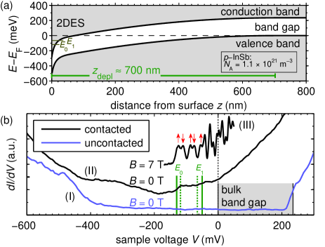
Applying a magnetic field perpendicular to the 2DES results in peaks corresponding to Landau levels (LLs) and spin levels of the 2DES [curve (III), Fig. 1(b)]. Their distance is in accordance with the effective mass and -factor of the InSb conduction band sup . The width of the peaks at lower energy is which is caused by the potential disorder, mainly given by the dopants of the substrate. The Cs atoms, which are ionized by only Getzlaff et al. (2001), have a minor effect Morgenstern et al. (2002a).
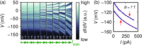
Further evidence for the electrical decoupling of the 2DES from the BVB is presented in Fig. 2, where curves at increasing are shown for different . All curves are measured at the same lateral position. With increasing , pairs of lines corresponding to spin split LLs appear. For , increasing does not change the spectra. At higher the spectra are spread in with increasing . At , the spin splitting of the lowest LL is increased by 13 % and the LL distance is increased by 18 %. The spreading is symmetric around , i.e. around . It is attributed to the increased localization of electrons with growing leading to a decrease of 2D conductivity Prange and Girvin (1986). The spreading cannot be explained by tip induced band bending (Stark effect) Feenstra and Stroscio (1987); *Dombrowski1999, which might increase with due to a reduced screening of the 2DES. Poisson calculations reveal that the spreading at largest tip–surface distance must be much larger than the spreading induced by the change in tip–surface distance in contrast to experiment. Instead, the spreading is quantitatively reproduced by assuming a thermally activated nearest neighbor hopping of the localized electrons within the 2DES from or towards the tip. The model uses barrier heights and next-neighbor distances of valleys as determined from spatially resolved data sup and assumes a reasonable attempt frequency of Hz 111Details will be subject of a forthcoming publication.. The resulting peak positions in comparison with the experimental data for are shown in Fig. 2(b). The excellent agreement strongly supports our assumption that the current indeed flows along the 2DES exhibiting reduced conductivity with increasing .
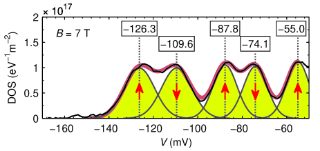
The surface 2DES, thus, is occupied, exhibits Landau as well as spin quantization, has moderate disorder, and is decoupled from the bulk electrons of InSb. Moreover, the center of mass of the 2DES is 8 nm below the surface and, thus, sufficiently far from the metallic tip to prevent complete screening. These are the requirements to observe e-e interaction effects within the QH regime. One such effect is the EE of the spin splitting. Loosely speaking the effective repulsion between electrons with parallel spins is smaller than the one for antiparallel spins. This eventually leads to an increase of the spin splitting energy at odd filling factors Ando and Uemura (1974). Fig. 3(a) shows spectra taken at a fixed position while ramping the magnetic field providing the so-called Landau fan.
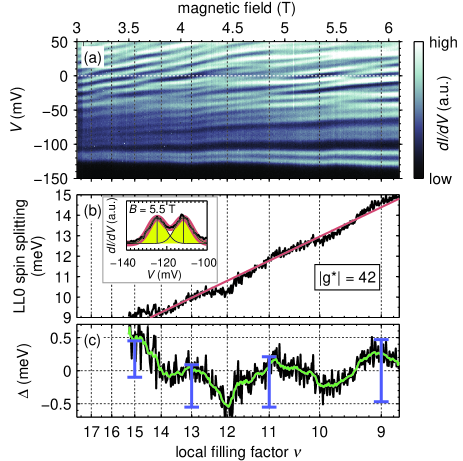
Less than 10 % of the fanning is caused by the spreading resistance described above. Varying , the conductance lines are wavy and deviate from with subband index , LL index , spin index , cyclotron frequency , and Bohr magneton . One obvious reason for waviness is a shift of with magnetic field taking place once the increasing degeneracy of a LL favors a transition to the next LL. More importantly, is filling factor dependent due to the EE. To analyze this in more detail, we concentrate on the lowest LL around , which gives the highest accuracy in determining . We adapted two Gaussians for all 386 spectra between and 222Gaussians of equal width and height were fitted using a nonlinear least squares method and a trust-region algorithm as implemented in Matlab, see MathWorks Curve Fitting Toolbox V2.1 User’s Guide. The fits are good as can be seen in the inset of Fig. 3(b) and by the confidence value of ( above ). The error for the resulting is about . is shown in Fig. 3(b) in comparison to a straight line corresponding to ordinary Zeeman splitting of with . Fig. 3(c) shows the deviation from the straight line. It oscillates around 0 meV with maxima (minima) around odd (even) filling factors as expected for EE Janak (1969). The not expected negative values of are probably caused by slight deviations from a spin splitting linear in due to either increasing spreading with , which leads to superlinearity, or nonparabolicity of InSb leading to a smooth decrease of , thus, supralinearity. However, both effects cannot explain oscillations in . One could imagine that spreading depends also on filling factor being largest at even ones, but that would lead to an oscillation with maxima at even filling factor.
Moreover, the amplitude of the oscillation is about in excellent agreement with theoretical estimates for EE [vertical bars in Fig. 3(c)]. They are obtained by treating the Coulomb interaction using a random phase approximation. This is well justified since the subband electron density is large compared to the scale set by the Bohr radius Ando and Uemura (1974); Smith et al. (1992a); sup . We performed the calculation using and but emphasize that the results barely change if these or other system parameters are varied within reasonable limits (e.g. less than 1 % for ). Thus, magnitude and oscillation phase of compare favorably with a parameter-free calculation of EE. This implies that the short-ranged e-e interaction effect EE can be probed by STS.
For localized electrons interacting via the long-ranged part of the Coulomb repulsion, the averaged tunneling DOS is expected to show a gap at Pollak (1970); Efros and Shklovskii (1975); Pikus and Efros (1995). For a 2DES with unscreened repulsion at K, a qualitative analysis gives Efros and Shklovskii (1975); Pikus and Efros (1995)
| (1) |
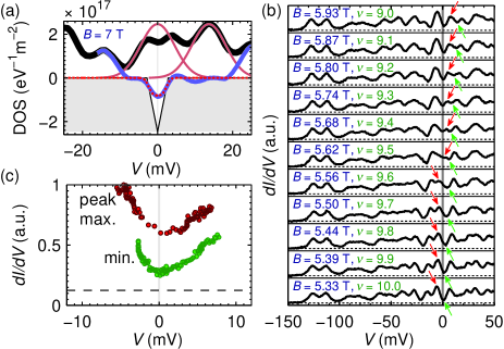
More elaborate analytical and numerical results leave no doubt about the existence of a Coulomb gap while the exact shape remains controversial Pikus and Efros (1995); Glatz et al. (2008). This is due to the underlying (spin-)glass physics Glatz et al. (2008) known to be notoriously complex. A linear Coulomb gap was deduced from various experiments Butko et al. (2000); *Ashoori; *Ashoori2; *Hansen. In our case, where the ratio between disorder and e-e interaction is , we also find a dip in the DOS at . Fig. 4(a) shows the spatially averaged curve (thick line) at . Instead of a peak at , one observes a double-peak with a minimum at 0 mV. The sum of two identical Gaussian peaks (thin lines)—mimicking the two spin levels of this particular LL (see sup )—matches the measured DOS except of a suppression at . Taking the difference between measured DOS and the sum of the two Gaussians eliminates all single-particle effects leaving only the dip at (medium line). If we modify Eq. (1) to account for finite temperature and screening effects Pikus and Efros (1995) as well as for the energy resolution of our experiment of sup , we obtain the dotted curve in Fig. 4(a). It shows excellent agreement with the measured dip. The screening is taken to be caused by the STM tip being 8.6 nm away from the center of mass of the 2DES sup . Note that we observe the gap even around the critical state, i.e., close to half filling of a spin-polarized LL, which is consistent with numerical studies Yang and MacDonald (1993). The facts that we do not observe the dip at without localization (at ) and that we can reproduce it by a reasonable, parameter-free calculation strongly suggests that we observe the Coulomb gap. We can rule out inelastic excitations as a cause which would lead to much larger half widths of the gap (optical phonons: 22 meV, plasmons: 60 meV, spin excitations: 18 meV) and we are not aware of any many-particle mechanism besides the long-ranged Coulomb repulsion of localized electrons leading to a gap with the observed characteristics.
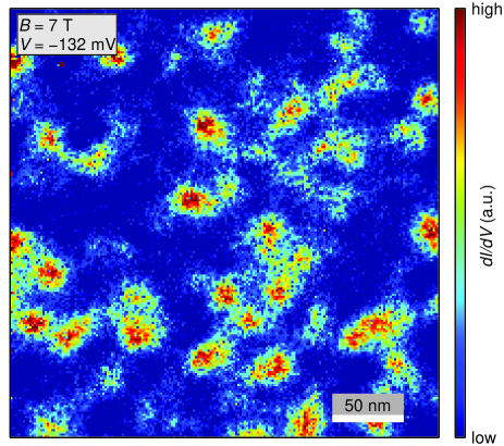
Surprisingly, a Coulomb gap—although typically thought of being a phenomenon related to disorder averaging or spatial averaging—is also observed in the local DOS Morgenstern et al. (2002b). The intensity of a particular LDOS peak is suppressed when moved through by increasing . Fig. 4(b) shows corresponding curves at fixed position. The upper arrows follow a single spin level as it crosses and the peak intensity is plotted in Fig. 4(c). A minimum intensity is observed exactly at () where the peak is suppressed by (suppression in averaged DOS: ). The same kind of suppression is found for the minimum between LLs, which is marked by the lower lying arrows in (b) and plotted in (c), too. A suppression at is also found for fixed , if different positions are probed within the potential landscape sup . The finding of Coulomb suppression in the LDOS requires further studies and might be related to Coulomb glass dynamics Menashe et al. (2001).
In summary, we have shown that low-temperature STS is able to detect e-e interaction in QH samples down to a resolution below all relevant length scales. We have found an exchange enhancement (EE) of the spin splitting at odd fillings and a Coulomb suppression of the averaged as well as of the local DOS at . The EE is in quantitative agreement with a well justified theory, while, due to the less clear status of theory, the comparison for the Coulomb gap is with calculations based on qualitative arguments only. No well-developed theory for the LDOS exists and we conjecture that the Coulomb gap in LDOS is related to (spin-)glass physics.
We acknowledge support by the DFG (MO 858/11-1).
I Supplementary Information
II Experimental details
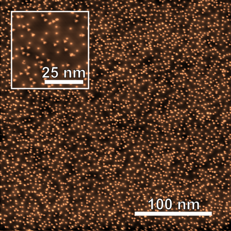
For sample preparation, we glued a p-InSb single crystal of size to a sample holder using silver epoxy. A silver epoxy line drawn at one side of the crystal from the sample holder towards the surface serves as a direct electrical contact to the 2DES. At the opposite side of the epoxy line, the crystal was cut for controlled cleavage about in depth. This cut is parallel to the sample holder surface and located about above the sample holder. After bake-out within the load-lock of our ultrahigh vacuum system, the crystal was cleaved at room temperature and a pressure of exhibiting the (110) surface. Then, we transferred the crystal into the pre-cooled scanning tunneling microscope (STM). For this purpose, the STM was lifted from the bath cryostat to the transfer chamber without breaking the vacuum Mashoff et al. (2009). Cesium from a well-outgassed dispenser (SAES Getters) was evaporated onto the cold crystal surface. During and after the adsorption process the sample was held below to prevent diffusion induced Cs clustering Becker et al. (2010). Fig. S1 shows a resulting STM image. The image area is atomically flat and each bright dot corresponds to a single cesium atom or, partly, to a Cs dimer which both act as donors. 3300 adsorbates are visible which corresponds to a coverage of per InSb(110) surface unit cell.
The STM tip was etched from a tungsten wire outside of the vacuum system and prepared within the STM by field emission and consecutive voltage pulses on a W(110) crystal as well as on the InSb(110) surface itself. After such voltage pulses on InSb, the scan area had to be changed using the translation stage of the STM. We used tungsten because it enabled us to give good results on a similar sample system not exhibiting tip-induced band bending Becker et al. (2010).
III Landau levels and potential disorder
At , we observe the spin split Landau levels of the first subband as shown in Fig. 1(b) of the main article. The same measurement is shown in Fig. S2 with the corresponding Gaussian fits.
From the positions of the fits we extract a spin splitting for the first Landau level of giving an effective Landé g-factor of . From the mean difference of the first two Landau levels we get an effective mass of (: free electron mass). These values are in good agreement with previous STS measurements on InSb Hashimoto et al. (2008); Becker et al. (2010) and differ slightly from the known low temperature values for InSb at the conduction band minimum Vurgaftman et al. (2001) and Madelung et al. (2002) due to the well-known nonparabolicity of the conduction band of InSb.
The full width at half maximum (FWHM) of the fits decreases with Landau level index , being for , for and for the first spin level of . This effect is due to the decreased sensitivity of the Landau level drift states to the potential landscape, which can only probe potential fluctuations down to length scales of Hashimoto et al. (2008). Single spot spectra only show a width of about for . From this, we can estimate the width of the potential disorder to be .
The main cause for the potential disorder are the charged acceptors within the subband layer. The potential disorder of a highly doped p-InSb(110) sample covered with Cs has been larger with meV Becker et al. (2010). A previously analyzed 2DES prepared by Cs coverage on n-InSb(110) showed a potential disorder comparable to our system with meV, deduced from the lowest spin level at and Hashimoto et al. (2008). The disorder of a 2DES created by Fe adsorption on n-InAs(110) showed a potential disorder of about Morgenstern et al. (2002a, 2003), which was determined by two independent methods: an STM image of the potential landscape was generated by probing the surface with a tip-induced quantum dot state Morgenstern et al. (2002a) and FWHM of Landau level peaks measured at and were evaluated Morgenstern et al. (2003). However, these measurements are not spin resolved due to the lower -factor of InAs, so a direct comparison of is difficult.
The lateral distribution of the potential disorder can be imaged by scanning tunneling spectroscopy (STS) in real space as is shown in Fig. S3.
The voltage of this image corresponds to the onset of the first Landau level and, thus, a high intensity exhibits the potential pits. There are roughly 40 local potential minima within the imaged area, giving an average distance of in accordance with visual inspection.
IV Band bending and subband calculation
It is well-known that submonolayer amounts of atoms adsorbed on an InSb surface lead to a large band bending near the surface. The adsorbed atoms act as donors to the underlying substrate with a donor level in the conduction band. For cesium on n-InSb(110), this donor level has been determined by photoelectron spectroscopy to be above the conduction band minimum Betti et al. (2001). In our case of p-doped InSb, where the bulk Fermi level lies at the valence band edge, we have to add the low temperature band gap of Vurgaftman et al. (2001) to get an estimate of the total band shift at the surface of . The corresponding band bending leads to electrons within an inversion layer which form two-dimensional subbands. The curvature of the potential inside the semiconductor, therefore, depends on the charge distribution within the inversion layer and on the density of charged acceptors.
The sample we used has an acceptor concentration of , which is orders of magnitude lower than the inversion layer electron concentration. To get an estimate of the expected subband energies without having to solve the Poisson equation and the full Hamiltonian including the nonparabolicity of InSb self-consistently, we approximate the inversion layer distribution by the 3D bulk density of states:
| (S1) |
The energy dependence of the effective mass due to the nonparabolicity is approximated by Merkt and Oelting (1987) with the known effective mass at the conduction band minimum Vurgaftman et al. (2001). This results in a band bending as shown in Fig. 1(a) of the main article with an inversion layer electron concentration of .
To obtain the subband positions , within this potential, we use the triangular well approximation Ando et al. (1982) with electric fields approximated by the mean slope of the potential up to and an effective mass using the approximation Merkt and Oelting (1987). Here, the energy splits up into the in-plane energy and the energy at the onset of the subbands. The subband positions are marked in Fig. 1(a) by horizontal lines. The density of subbands above the Fermi level is relatively large because of the flat band bending at a depth beyond the inversion layer, where only the acceptor density can screen the electric field. The first two subbands and are in good agreement with the experiment as shown in Fig. 1(b).
The 2D electron concentrations of the first two subbands are and . Their electron distributions along are plotted in Fig. S4.
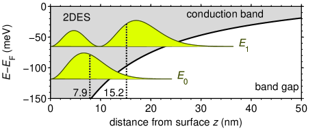
From these distributions, the mean depth of the subband electrons below the surface is deduced to be for the first subband and for the second subband.
The averaged curve (curve (II) of Fig. 1(b)) exhibits rounded steps close to the energies calculated by the Poisson-Schrödinger equation. The width of these steps is caused by disorder. Indeed, spatially resolved images as shown e.g. in Fig. 3 of Ref. Morgenstern et al. (2002a) reveal quantum dot like states at low energy which percolate close to the onset of the plateau. The decreasing height of the step with increasing subband index is consistently observed for different 2DES Morgenstern et al. (2002a); Wiebe et al. (2003); Becker et al. (2010) and is attributed to the fact that higher subbands are reaching deeper into the crystal and, thus, have a lower LDOS at the surface. This is clearly visible in Fig. S4.
V Coulomb gap and energy resolution
In order to account for the finite temperature and for screening effects by the metallic STM tip, we have modified the V-shaped DOS of Eq. (1) of the main article called by a finite DOS at according to Ref. Pikus and Efros, 1995:
| (S2) |
with being the distance of a metallic gate to the center of the 2DES and being the Boltzmann constant. In our system, can be estimated by the mean depth of the first subband as calculated above and the distance of the STM tip to the surface. The distance of the tip to the surface is estimated by fitting measurements to an exponential tunneling decay and extrapolating the offset to the quantum of conductance with electron charge and Planck’s constant Kröger et al. (2007). From this, we get a tip distance of about at the stabilizing current of this measurement . This results in . With Dixon and Furdyna (1980), we get . For the sake of simplicity, we simply cut off the V-shaped Coulomb gap by this value leading to .
The Coulomb gap is finally broadened by the energy resolution of the STS experiment being Wachowiak (2003); Haude (2001) with and . In order to calculate the resulting curve, we approximate a Gaussian energy broadening with being twice its standard deviation. This Gaussian is folded with the calculated resulting in the red dotted curve of Fig. 4(a) of the main article. Notice that no fit parameter is involved within this calculation which excellently reproduces the measured Coulomb gap.
VI Local Coulomb gap within the potential landscape
The Coulomb gap in the DOS has been measured and discussed within the main article via spatially averaged spectra. The main article and the attached video file shows, in addition, that single peaks measured at a fixed position also exhibit a Coulomb gap, i.e. a reduction of intensity while moved across by field. Such a Coulomb gap can also be identified at fixed magnetic field in local spectra taken at different positions within the potential landscape.
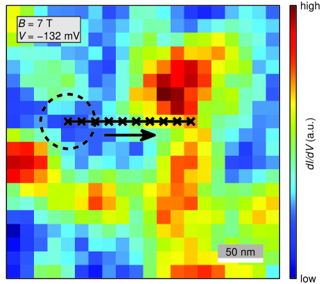
Fig. S5 shows a low energy image marking the potential disorder of the same area as imaged in Fig. S3. Fig. S5 has lower spatial resolution, but higher energy resolution. The averged spectrum of all spectra gives the DOS of Fig. 1(b)(III) of the main article. Each pixel represents a spatial average of 12 neighboring spectra, thus exhibiting the averaged potential of an area of about . The spectra corresponding to the marked positions are shown in Fig. S6.
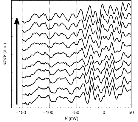
Moving down in the potential landscape as indicated by the arrow, the peaks belonging to the three lowest Landau levels shift to lower energies as expected. Near the Fermi level, additional subbands lead to a more irregular pattern, but the Landau levels of the lowest subband still dominate the pattern. If observed carefully, all features shift to lower energies, except the suppression caused by the Coulomb gap, which is pinned to . This suppression is visible as a dip at medium potential, where a spin state is exactly at , and as kinks in the tails of the peaks at low and high potential. This plot illustrates again the local observation of a Coulomb gap feature, now by averaging over distances belonging to a single potential minimum or maximum. Thus, the Coulomb gap appears to be ubiquitous even in local spectra, which is not expected from the typical qualitative arguments.
VII Theoretical estimate of the exchange enhancement
In this Section, we briefly sketch how to obtain a quantitative estimate of the filling factor dependence of the effective -factor resulting from the Coulomb interaction. We start out by introducing the Hamiltonian describing a two-dimensional free electron gas subject to a perpendicular magnetic field (pointing in -direction):
| (S3) |
with being an annihilation operator in second quantization. The single-particle energies read
| (S4) |
where the effective mass and effective -factor can both be extracted from our experimental data. We have chosen the vector potential in the Landau gauge, and the -th Landau level of electrons with spin is thus characterized by an additional quantum number associated with the momentum operator of the -direction. In contrast, the interaction is naturally expressed in terms of two-dimensional momentum quantum numbers :
| (S5) |
Using cgs units, the Fourier transform of the Coulomb potential yields
| (S6) |
with the form factor accounting for the finite thickness of the inversion layer Ando and Uemura (1974):
| (S7) |
The dielectric constant of InSb is given by , and as well as are the total electron density in the inversion layer as well as the density of the ionized acceptors, respectively.
In order to compute the self-energy of the many-particle problem posed by the Hamiltonian , we employ the random phase approximation (RPA) Ando and Uemura (1974), which is reasonable for the problem at hand (at least for integer filling factors where the fractional quantum Hall effect is absent) since the density of the electrons occupying the lowest subband is large compared to the scale set by the Bohr radius . The first (Fock exchange Janak (1969)) term of the RPA series reads
| (S8) |
where is the noninteracting Matsubara Green function related to , the magnetic length, and as well as denote the temperature and the chemical potential, respectively. We have defined the following combination of associated Laguerre polynomials :
| (S9) |
In order to derive the second equality of Eq. (S8), one needs to evaluate the two-particle matrix element of the Coulomb interaction. This can be achieved by resorting to the momentum representation of the Landau states ,
| (S10) |
inserting unit operators, and eventually carrying out an integral over products of Hermite polynomials Gradstein and Ryshik (1981).
The second term of the RPA series involves the bubble diagram depicted in Fig. S7. The corresponding analytic expression reads
| (S11) |
with being the Fermi function. The second equality can again be established by inserting unit operators in order to calculate the (two-dimensional) momentum matrix elements of the noninteracting Green function. Since Eq. (S11) is of the same (momentum-conserving) structure as the Coulomb potential, the geometric RPA series can be summed up in complete analogy with the well-known case where the magnetic field is absent Bruus and Flensberg (2004). The resulting self-energy is eventually given by Eq. (S8) with the bare replaced by
| (S12) |
which we moreover set to its zero-frequency value Ando and Uemura (1974). The remaining Matsubara sum in Eq. (S8) can then be carried out analytically, and the self-energy (which is frequency-independent, ruling out difficulties with the analytic continuation to the real axis from the beginning) can be computed with minor numerical effort. Surprisingly, it turns out that such a static screening approximation is sufficient to reproduce the results of more elaborate approaches Smith et al. (1992b) on a quantitative level, providing the a posteriori motivation to solely stick to this scheme.

Since the self-energy is diagonal MacDonald et al. (1986) w.r.t. and , the magnitude of the oscillations shown in Fig. 4(c) of the main text is given by
| (S13) |
where the two bracketed terms are to be computed at filling factors and , respectively. The result is , in nice agreement with the experimental data. We emphasize that these values only change slightly when the physical system parameters (such as the dielectric constant, the temperature, the effective -factor, or the effective mass) are varied within reasonable limits. E.g., using instead of leads to , .
References
- Klitzing et al. (1980) K. v. Klitzing, G. Dorda, and M. Pepper, Phys. Rev. Lett. 45, 494 (1980).
- Prange and Girvin (1986) R. E. Prange and S. M. Girvin, Quantum Hall Effect (Springer, Berlin, 1986).
- Du et al. (2009) X. Du, I. Skachko, F. Duerr, A. Luican, and E. Y. Andrei, Nature 462, 192 (2009).
- Bolotin et al. (2009) K. I. Bolotin, F. Ghahari, M. D. Shulman, H. L. Stormer, and P. Kim, Nature 462, 196 (2009).
- Song et al. (2010) Y. J. Song, A. F. Otte, Y. Kuk, Y. Hu, D. B. Torrance, P. N. First, W. A. de Heer, H. Min, S. Adam, M. D. Stiles, A. H. MacDonald, and J. A. Stroscio, Nature 467, 185 (2010).
- Levy et al. (2010) N. Levy, S. A. Burke, K. L. Meaker, M. Panlasigui, A. Zettl, F. Guinea, A. H. C. Neto, and M. F. Crommie, Science 329, 544 (2010).
- Tsui et al. (1982) D. C. Tsui, H. L. Stormer, and A. C. Gossard, Phys. Rev. Lett. 48, 1559 (1982).
- Lilly et al. (1999) M. P. Lilly, K. B. Cooper, J. P. Eisenstein, L. N. Pfeiffer, and K. W. West, Phys. Rev. Lett. 82, 394 (1999).
- Barrett et al. (1995) S. E. Barrett, G. Dabbagh, L. N. Pfeiffer, K. W. West, and R. Tycko, Phys. Rev. Lett. 74, 5112 (1995).
- Aristov et al. (1994) V. Y. Aristov, G. LeLay, P. Soukiassian, K. Hricovini, J. E. Bonnet, J. Osvald, and O. Olsson, Europhys. Lett. 26, 359 (1994).
- Morgenstern et al. (2002a) M. Morgenstern, J. Klijn, C. Meyer, M. Getzlaff, R. Adelung, R. A. Römer, K. Rossnagel, L. Kipp, M. Skibowski, and R. Wiesendanger, Phys. Rev. Lett. 89, 136806 (2002a).
- Morgenstern et al. (2003) M. Morgenstern, J. Klijn, C. Meyer, and R. Wiesendanger, Phys. Rev. Lett. 90, 056804 (2003).
- Hashimoto et al. (2008) K. Hashimoto, C. Sohrmann, J. Wiebe, T. Inaoka, F. Meier, Y. Hirayama, R. A. Römer, R. Wiesendanger, and M. Morgenstern, Phys. Rev. Lett. 101, 256802 (2008).
- Champel and Florens (2009) T. Champel and S. Florens, Phys. Rev. B 80, 161311(R) (2009).
- Miller et al. (2010) D. L. Miller, K. D. Kubista, G. M. Rutter, M. Ruan, W. A. de Heer, M. Kindermann, P. N. First, and J. A. Stroscio, Nat. Phys. 6, 811 (2010).
- Niimi et al. (2009) Y. Niimi, H. Kambara, and H. Fukuyama, Phys. Rev. Lett. 102, 026803 (2009).
- Luican et al. (2011) A. Luican, G. Li, and E. Y. Andrei, Phys. Rev. B 83, 041405(R) (2011).
- Pollak (1970) M. Pollak, Discuss. Faraday Soc. 50, 13 (1970).
- Efros and Shklovskii (1975) A. L. Efros and B. I. Shklovskii, J. Phys. C 8, L49 (1975).
- Pikus and Efros (1995) F. G. Pikus and A. L. Efros, Phys. Rev. B 51, 16871 (1995).
- Eisenstein et al. (2002) J. P. Eisenstein, K. B. Cooper, L. N. Pfeiffer, and K. W. West, Phys. Rev. Lett. 88, 076801 (2002).
- Mashoff et al. (2009) T. Mashoff, M. Pratzer, and M. Morgenstern, Rev. Sci. Instrum. 80, 053702 (2009).
- (23) See supplementary information in the second part of the document and movie in ancillary files.
- Betti et al. (2001) M. G. Betti, V. Corradini, G. Bertoni, P. Casarini, C. Mariani, and A. Abramo, Phys. Rev. B 63, 155315 (2001).
- Kanisawa et al. (2001) K. Kanisawa, M. J. Butcher, H. Yamaguchi, and Y. Hirayama, Phys. Rev. Lett. 86, 3384 (2001).
- Wiebe et al. (2003) J. Wiebe, C. Meyer, J. Klijn, M. Morgenstern, and R. Wiesendanger, Phys. Rev. B 68, 041402(R) (2003).
- Becker et al. (2010) S. Becker, M. Liebmann, T. Mashoff, M. Pratzer, and M. Morgenstern, Phys. Rev. B 81, 155308 (2010).
- Masutomi et al. (2007) R. Masutomi, M. Hio, T. Mochizuki, and T. Okamoto, Appl. Phys. Lett. 90, 202104 (2007).
- Ando (1984) T. Ando, J. Phys. Soc. Jpn. 53, 3101 (1984).
- Vurgaftman et al. (2001) I. Vurgaftman, J. R. Meyer, and L. R. Ram-Mohan, J. Appl. Phys. 89, 5815 (2001).
- Getzlaff et al. (2001) M. Getzlaff, M. Morgenstern, C. Meyer, R. Brochier, R. L. Johnson, and R. Wiesendanger, Phys. Rev. B 63, 205305 (2001).
- Feenstra and Stroscio (1987) R. M. Feenstra and J. A. Stroscio, J. Vac. Sci. Technol. B 5, 923 (1987).
- Dombrowski et al. (1999) R. Dombrowski, C. Steinebach, C. Wittneven, M. Morgenstern, and R. Wiesendanger, Phys. Rev. B 59, 8043 (1999).
- Note (1) Details will be subject of a forthcoming publication.
- Ando and Uemura (1974) T. Ando and Y. Uemura, J. Phys. Soc. Jpn. 37, 1044 (1974).
- Note (2) Gaussians of equal width and height were fitted using a nonlinear least squares method and a trust-region algorithm as implemented in Matlab, see MathWorks Curve Fitting Toolbox V2.1 User’s Guide.
- Janak (1969) J. F. Janak, Phys. Rev. 178, 1416 (1969).
- Smith et al. (1992a) A. P. Smith, A. H. MacDonald, and G. Gumbs, Phys. Rev. B 45, 8829(R) (1992a).
- Glatz et al. (2008) A. Glatz, V. M. Vinokur, J. Bergli, M. Kirkengen, and Y. M. Galperin, J. Stat. Mech.: Theory Exp. 2008, P06006 (2008).
- Butko et al. (2000) V. Y. Butko, J. F. DiTusa, and P. W. Adams, Phys. Rev. Lett. 84, 1543 (2000).
- Ashoori et al. (1993) R. C. Ashoori, J. A. Lebens, N. P. Bigelow, and R. H. Silsbee, Phys. Rev. B 48, 4616 (1993).
- Chan et al. (1997) H. B. Chan, P. I. Glicofridis, R. C. Ashoori, and M. R. Melloch, Phys. Rev. Lett. 79, 2867 (1997).
- Deviatov et al. (2000) E. V. Deviatov, A. A. Shashkin, V. T. Dolgopolov, W. Hansen, and M. Holland, Phys. Rev. B 61, 2939 (2000).
- Yang and MacDonald (1993) S.-R. E. Yang and A. H. MacDonald, Phys. Rev. Lett. 70, 4110 (1993).
- Morgenstern et al. (2002b) M. Morgenstern, D. Haude, J. Klijn, and R. Wiesendanger, Phys. Rev. B 66, 121102(R) (2002b).
- Menashe et al. (2001) D. Menashe, O. Biham, B. D. Laikhtman, and A. L. Efros, Phys. Rev. B 64, 115209 (2001).
- Madelung et al. (2002) O. Madelung, U. Rössler, and M. Schulz, Landolt-Börnstein - Group III Condensed Matter (Springer Verlag, 2002).
- Merkt and Oelting (1987) U. Merkt and S. Oelting, Phys. Rev. B 35, 2460 (1987).
- Ando et al. (1982) T. Ando, A. B. Fowler, and F. Stern, Rev. Mod. Phys. 54, 437 (1982).
- Kröger et al. (2007) J. Kröger, H. Jensen, and R. Berndt, New J. Phys. 9, 153 (2007).
- Dixon and Furdyna (1980) J. R. Dixon and J. K. Furdyna, Solid State Commun. 35, 195 (1980).
- Wachowiak (2003) A. Wachowiak, Aufbau einer 300 mK-Ultrahochvakuum-Rastertunnelmikroskopie-Anlage mit 14 Tesla Magnet und spinpolarisierte Rastertunnelspektroskopie an ferromagnetischen Fe-Inseln, Ph.D. thesis, Universität Hamburg (2003).
- Haude (2001) D. Haude, Rastertunnelspektroskopie auf der InAs(110)-Oberfläche: Untersuchungen an drei-, zwei- und nulldimensionalen Elektronsystemen im Magnetfeld, Ph.D. thesis, Universität Hamburg (2001).
- Gradstein and Ryshik (1981) I. S. Gradstein and I. M. Ryshik, Summen-, Produkt- und Integral-Tafeln, Band 2 / Tables of Series, Products, and Integrals, Volume 2 (Verlag Harry Deutsch, Frankfurt/Main, 1981).
- Bruus and Flensberg (2004) H. Bruus and K. Flensberg, Many-Body Quantum Theory in Condensed Matter Physics (Oxford University Press, New York, 2004).
- Smith et al. (1992b) A. P. Smith, A. H. MacDonald, and G. Gumbs, Phys. Rev. B 45, 8829 (1992b).
- MacDonald et al. (1986) A. H. MacDonald, H. C. A. Oji, and K. L. Liu, Phys. Rev. B 34, 2681 (1986).