Gaps tunable by electrostatic gates in strained graphene
Abstract
We show that when the pseudomagnetic fields created by long wavelength deformations are appropriately coupled with a scalar electric potential, a significant energy gap can emerge due to the formation of a Haldane state. Ramifications of this physical effect are examined through the study of various strain geometries commonly seen in experiments, such as strain superlattices and wrinkled suspended graphene. Of particular technological importance, we consider setup where this gap can be tunable through electrostatic gates, allowing for the design of electronic devices not realizable with other materials.
I Introduction
GrapheneNovoselov et al. (2004, 2005) is a material whose unique properties are a fascinating challenge in both fundamental and applied sciences. The basic properties of its electronic structure are chirality, electron-hole symmetry, and linear gapless energy spectrum, that is, charge carriers in graphene are massless Dirac fermionsCastro Neto et al. (2009). In addition, corrugations and topological defects create gauge (pseudomagnetic and even pseudo-gravitational) fields acting on electron statesVozmediano et al. (2010).
Recently, a novel state of matter, a quantum Hall insulator without a macroscopic magnetic field (Haldane stateHaldane (1988)), has spawned the interest in unusual topological properties of band structures, leading to the prediction of topological insulators in two and three dimensionsKane and Mele (2005); Fu et al. (2007); Qi and Zhang (January 2010); Moore (2010); Hasan and Kane (2010). It was understood afterwards that such Haldane state can be realized in a graphene superlattice by a suitable combination of scalar and vector electromagnetic potentialsSnyman (2009). A gap opens in the electronic spectrum, turning graphene into a quantum Hall insulator with protected chiral edge states. Since, long wavelength strains in graphene induce a pseudomagnetic gauge fieldnot ; Guinea et al. (2010), the combination of strains and a scalar potential should too open a gap in graphene111In contrast with the real magnetic field, strains do not break time reversal symmetry, and the resulting insulator is not a strong topological insulator - there is a pair of counterpropagating edge states belonging to different valleys, however, the intravalley scattering is frequently very weak which make these states well protected, similar to the case considered in Ref.Guinea et al. (2010). Although strong edge disorder would leads to a transport gap insteadLow and Guinea (2010), which might be technologically useful too. . The latter, if realised, would be of general interest. This is the subject of our work.
Energy gap in graphene is crucial for many applications. Its realization remains a challenging problem, as the transformation of electrons into holes i.e. Klein tunnelingKatsnelson et al. (2006), is an significant obstacle. At present, all known ways of gap opening have a detrimental effect on the electron mobility. In both biased bilayer and chemically functionalized graphene, one arrives at a disordered semiconductor with Mott variable range hopping mobility Taychatanapat and Jarillo-Herroro (2010); Elias et al. (2009); Nair et al. (2010). In graphene nanoribbons, the mobility is typically several order of magnitude smaller than in bulk graphene Han et al. (2010). Our approach provides an attractive route to circumvent these limitations and might also allows for the design of new electronic devices.
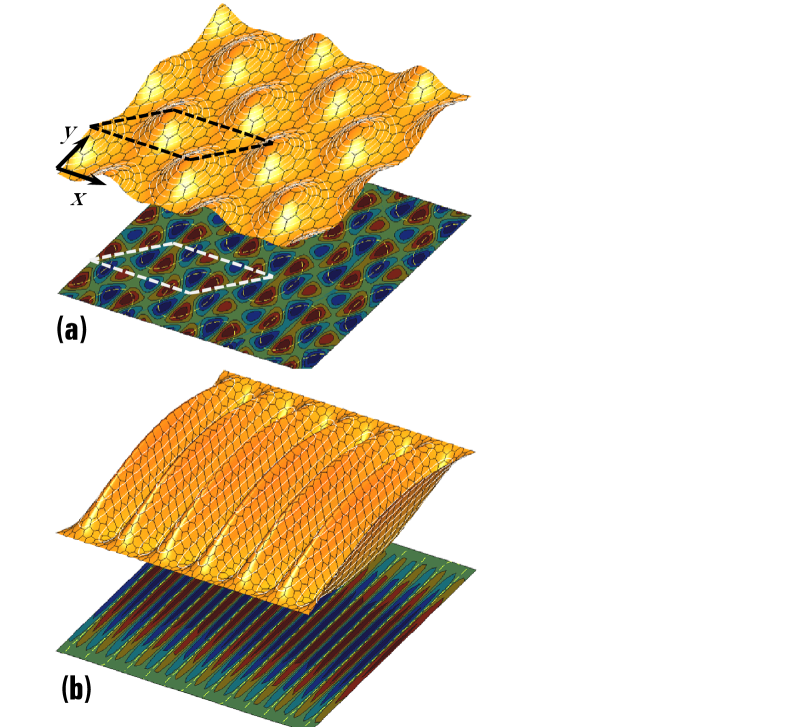
This paper is organized as follows. In Sec. II, we present a general argument for the gap opening due to combination of strains and a scalar potential. Sec. III considers specific realization of this effect in strain superlattices and wrinkles, Fig. 1 provide an illustrations of these two strain geometries. In particular, we consider physical setup where this gap can be tunable through electrostatic gates. Sec. IV considers related effects such as Fermi velocity renormalization, topological defects and interplay with magnetic field.
II General arguments
Strain induces scalar and gauge potentials in grapheneVozmediano et al. (2010). Fig. 1 illustrates the strain induced pseudo magnetic field for a strain superlattice and wrinkled graphene. In terms of the strain tensor, the scalar and vector potentials areSuzuura and Ando (2002); Mañes (2007); Vozmediano et al. (2010):
| (1) |
where eVChoi et al. (2009), Heeger et al. (1988), eV is the hopping between orbitals in nearest neighbor carbon atoms, and Å is the distance between nearest neighbor atoms.
The Hamiltonian for Dirac fermions in graphene, including a scalar potential and gauge fields due to strains is given by
| (2) |
where is the Fermi velocity, and and are Pauli matrices which operates on the sublattice and valley indices.
Using perturbation theory in both scalar and vector potential, we obtain a self energy correction which can be written as a cross-term to the Hamiltonian (linear in and linear in ):
| (3) | |||||
where the identity matrix is made explicit. Since the self energy contains term proportional to , a gap can be opened in both valleys. Next we make explicit the necessary relations between the scalar and gauge potential for this gap opening.
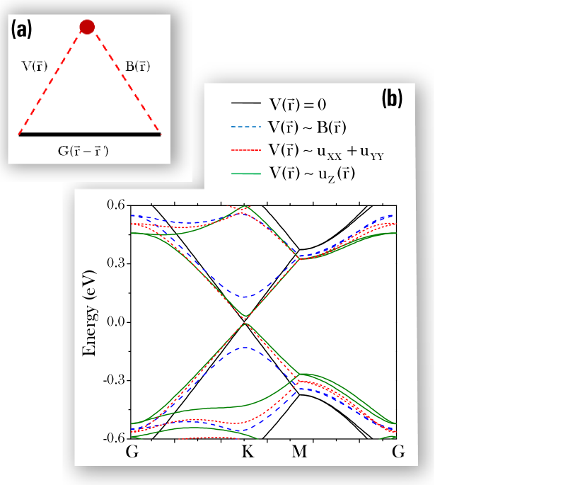
We calculate the second order diagram for the electron self energy (effective potential) as shown in Fig. 2a. At low energies, , and zero wave vector (corresponding to the Dirac point), the form for the induced gap reads
| (4) |
where is the commutator, and are Fourier components of scalar and vector potentials, respectively. This equation shows that the gap is induced through the correlations between the scalar potential and the pseudomagnetic (synthetic magnetic) field, . We characterize these correlations by the parameter such that
| (5) |
or, alternatively,
| (6) |
The parameter has dimensions of energy. It is roughly given by the value of the scalar potential times the number of flux quanta due to the synthetic field over the region where the field and the scalar potential are correlated. For , the integral in Eq. (4) diverges as . Then, the lower limit of the integral should be , turning Eq. (4) into a self consistent equation for .
In the diffusive regime, where electrons with momentum have an elastic scattering time , the divergence in the integral in Eq. (4) has to be cutoff at a momentum such that . For a periodic superlattice, the integral in Eq. (4) has to be replaced by a sum over reciprocal lattice vectors, . For graphene in the diffusive regime, resonant scatterersStauber et al. (2007); Wehling et al. (2010) or substrate chargesNomura and MacDonald (2007); Adam et al. (2007) give rise to a dependence , where is the concentration of scatterers, so that the lower cutoff in Eq. (4) is . Using this cutoff, we can write
| (7) |
where is the distance between nearest carbon atoms, which sets the scale of the high momentum limit in Eq. (4). Next, we extend this general argument to specific examples.
III Possible physical realizations
III.1 Global gap in strain superlattices
We show results for the gap opening due to correlation between the synthetic magnetic field and a scalar potential in strain graphene superlattice. We assume that the graphene layer is corrugated, as depicted in Fig. 1a. Depending on the lattice mismatch with the underlying substrate, the supercell size could vary from (e.g. iridium) to (e.g. boron nitride) times that of graphene unit cell. Here, we assumed supercell to be . The in-plane displacements were relaxed in order to minimize the elastic energy. Details of the implementation based on continuum elasticity model are given in Appendix A.
After minimizing the elastic energy, the resultant strains lead to an underlying non-homogeneous pseudomagnetic field as depicted in Fig. 1a. Fig. 2b shows the calculated electronic bandstructure of the superlattice, after considering various types of scalar potentials. Strain alone, , does not produce a gap. Although strains can induced a scalar potential of type , the correlation between this potential and the synthetic magnetic field due to the same strains is also zero. On the other hand, a scalar potential proportional to the height corrugation, i.e. , leads to the appearance of a gap, albeit a small one. Such a scalar potential could be induced by the substrate through an existence of electric field perpendicular to the graphene layer Guinea and Low (2010). Graphene superlattices induced by commensuration effects between the mismatch in the lattice constants of graphene and the substrateZhou et al. (2007); Vázquez de Parga et al. (2008); Martoccia et al. (2008); Pan et al. (2008) will, in general lead to the effect considered here. The existence of a gap at the Dirac energy in strained graphene superlattice is also consistent with observations which show gaps in very clean samples which are commensurate with the substrateZhou et al. (2007); Li et al. (2009); Hasan and Kane (2010).
In essence, strains generally induce both scalar and vector potentials. However, cross correlations between the scalar potential and the synthetic magnetic field, as in Eq. (6), vanish in many cases. In particular, the gap should be zero if the system remains symmetric with respect to inversionnot . A significantly large gap is obtained when the scalar potential and pseudomagnetic field are perfectly correlated, as shown in Fig. 2b for the case when . This observation is consistent with the general arguments that we presented in Sec. II. See also Appendix A, where a general expression for in strain superlattice is derived.
Next, we examine a slightly different scenario, where electrostatic gates are used to engineer the scalar potential so as to realise the correlation with the underlying strain-induced pseudo magnetic field.
III.2 Local gap in strain superlattices through quantum transport calculations
Here, we examine numerically the effect a local electric scalar potential on the electronic transport properties of strained graphene superlattices. The Hamiltonian accounting for nearest neighbor interactions between orbitals is given byWallace (1947),
| (8) |
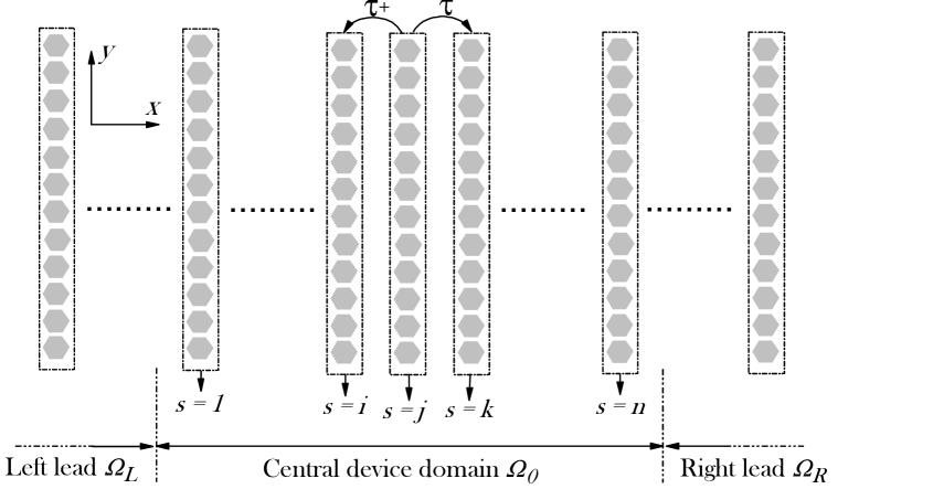
where is the on-site energy due to the scalar potential and is the hopping energy. is the new bond length after strain. To facilitate the application of various numerical techniques, the problem is partitioned into block slices as shown in Fig. 5. The retarded Green’s function in , the device region of interest, can then be written as (see Ventra (2008); Datta (1997); Haug and Jauho (2010) for general theory),
| (9) |
where is the Fermi energy, and are defined as and respectively. are the surface Green’s function, which can be obtained numerically through an iterative scheme Sancho et al. (1985) based on the decimation technique (see e.g. Guinea et al. (1983)). Various physical quantities of interest such as the transmission, current/charge density, local density-of-states can be obtained once is determined. See Appendix B for a more detailed description of the numerics.
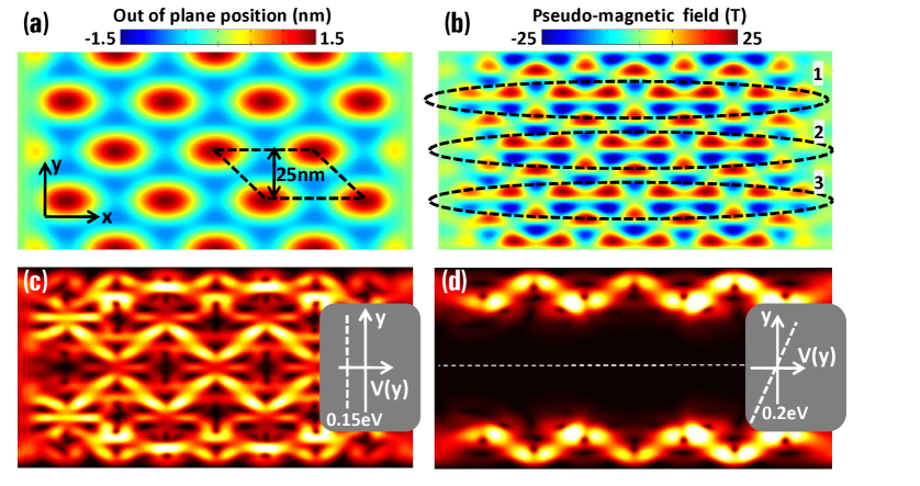
We consider a finite size strain superlattice of dimension , as depicted in Fig. 3a. The corresponding pseudomagnetic field is shown in Fig. 3b. Transport in non-homogeneous magnetic field is dominated by bulk “magnetic” states known as snake statesMartino et al. (2007). Snake states has been observed in high mobility 2D electron gas system, through controlled engineering of magnetic field via lithographic patterning of ferromagnetic or superconducting thin filmsYe et al. (1995); Nogaret and Bending (2000); Carmona et al. (1995).
Fig. 3c plots the current density due to current injection from the left contact, biased at Fermi energy of . As depicted, current flows in regions where , along the direction . Unlike the case of a real magnetic field, these snake states are non-chiral, with forward and backwards going states residing in opposite valleys. In the absence of short range scatterers, these states are relatively protected. Fig. 3b shows three conducting snake channels which forms the backbone for the conduction. Applying the general principle described in Sec. II, we apply a scalar potential that approximately correlates with the pseudomagnetic field of the middle channel to open up a local gap. Indeed, a local gap is opened, impeding current flow along this channel, as shown in Fig. 3d. Such a scalar potential can be realised experimentally with electrostatic side gates. This effect could be exploited in current guiding devices Williams et al. (2011).
III.3 Opening gaps in suspended graphene via wrinkles
Wrinkles are common feature in very clean suspended graphene samples, leading to finite strains. Partial control of these wrinkles can be achieved by adjusting the temperature, as in some cases, they are induced by the mismatch in thermal expansion coefficients between graphene and the substrateBao et al. (2009); Wang and Devel (2011). We assume that the deformation is described by the profile proposed in Cerda and Mahadevan (2003), as illustrated in Fig. 1a. The resulting synthetic field is discussed elsewhere Guinea et al. (2009). Fig. 1b illustrates the accompanied pseudo-magnetic field.
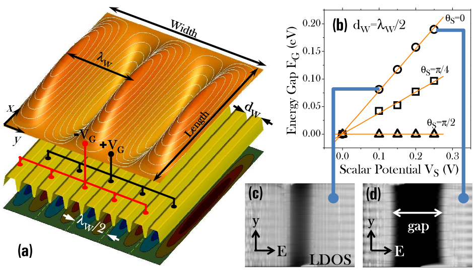
A sinusoidal-like scalar potential within graphene is induced by gates shown in Fig. 4a, which are tailored to correlate with the synthetic magnetic field induced by the strains. The results in Fig. 4b show that a gap is generated, whose magnitude is proportional to the scalar potential. We can estimate the gap induced by a combination of strains which are changed by over an area of spatial scale and a scalar potential of value on a region of the same size. The synthetic magnetic field is of order . Then
| (10) |
Eq. (10) is consistent with numerical results obtained in Fig. 4b. Fig. 4c and d clearly show the global nature of the gap generated. Effectively, the gate controlled gap allows the device in Fig. 4 to be operated as a graphene transistor.
Next, we consider situation where correlation is less than perfect. From Eq. (10), we note that even for small variations in the strain, , the gap can be of order of the potential fluctuations, , if the correlations between the scalar potential and the synthetic field are maintained over long distances, . Fig. 4b considers the case where there is a phase shift between the pseudomagnetic field and scalar potential. This corresponds to a decreasing in Eq. (10). Indeed the gap reduces as expected. In general, the presence of a gap is robust against reasonable degree of local disorder, since inversion symmetry is still absent in most part, see also Eq. (4) and related discussions.
IV Discussions
In this section we discuss several issues related with the previous consideration and the ways of further development.
IV.1 Renormalization of the Fermi velocity
As evident from Eq. (3), there are self energy corrections due to quadratic terms in the scalar and vector potentials. These terms lead to logarithmic corrections in the Fermi velocity via the renormalization of the residue of the Green function:
| (11) |
where is a momentum cutoff.
This renormalization has been previously found in non-linear sigma modelsFradkin (1986); Lee (1993); Nersesyan et al. (1994); Ziegler (1998). These logarithmic corrections also influence the kinetic equation which describes transport processesAuslender and Katsnelson (2007), in these terms they describe a pseudo-Kondo effect due to interband scattering (in the Dirac point, the energies of electron and hole states coincide which provides a necessary degeneracy). Due to these corrections, the Fermi velocity decreases in the presence of scalar and gauge disorder. When this effect is studied simultaneously with the increase induced by the Coulomb interaction non trivial new phases can ariseStauber et al. (2005); Herbut et al. (2008); Foster and Aleiner (2008).
IV.2 Gauge field due to topological defects
The sublattice and valley symmetries of graphene allow for the definition of a second gauge field, which hybridizes states from different valleys, and does not commute with the intravalley gauge field due to long wavelength strainsCastro Neto et al. (2009); Vozmediano et al. (2010). This field can be induced by topological defects, such as heptagons and pentagons. These defects are present at dislocations and grain boundaries, and they can be ordered periodically forming superlattices. If the synthetic magnetic field associated with this field is correlated with a scalar potential, a gap inducing term is generated.
The gauge field due to topological defects has the form
| (12) |
By using perturbation theory, as in Eq. (3), we obtain a self energy which is proportional to the cross correlations between the scalar potential and the gauge field, multiplied by the operator . Modulated Zeeman couplings can also lead to synthetic fields which act on the spin, allowing for the possibility of spin gaps as well.
IV.3 Interplay with magnetic field
The gap studied here is defined in the whole sample, although its value should be roughly inversely proportional to the ratio between the total area and the area where the synthetic magnetic field and scalar potential are correlated. The sign of the gap is determined by the scalar potential. Localized states will be formed at boundaries between regions where the gaps have different signs, similar to the edge states in topological insulators Qi and Zhang (January 2010); Moore (2010).
A periodic magnetic field, when correlated with a scalar potential leads to a gap whose signs are opposite in the two valleysSnyman (2009). A combination of this gap and the gap due to strains leads to gaps of different values in the two valleys, allowing for the control of the valley and sublattice degrees of freedom. For example, combined strain and synthetic magnetic field could be useful for valleytronicsLow and Guinea (2010). The realization of other synthetic fields might open new functionalities for graphene that cannot be achieved with other materials.
V Conclusion
We have discussed a novel way in which a combination of long wavelength strains and a long wavelength correlated potential can lead to a gap in the electronic spectrum of graphene. Such situation can occur naturally, because of correlations between a periodic substrate and graphene, or it can be engineered in a controlled way using electrostatic gates. Since the effect is induced by long wavelength, smooth perturbations, a gap can be induced without increasing the amount of scattering in the system. Finally, valley polarized edge states will be generated, as the band structure of the modified system resembles the spectrum of a quantum Hall insulator.
VI Acknowledgements
TL acknowledges funding from INDEX/NSF (US). FG acknowledges financial support from MICINN (Spain) through grants FIS2008-00124 and CONSOLIDER CSD2007-00010, and from the Comunidad de Madrid, through NANOBIOMAG. The work of MIK is part of the research program of the Stichting voor Fundamenteel Onderzoek der Materie (FOM), which is financially supported by the Nederlandse Organisatie voor Wetenschappelijk Onderzoek (NWO). Computational resources is provided by Network for Computational Nanotechnology (NCN) at Purdue University.
Appendix A Expression for energy gap in superlattice
Strains induce scalar and gauge potentialsVozmediano et al. (2010). We study the correlations between these potentials when the strains are induced by modulations in the vertical displacement of the layer, . We assume that the in plane displacements relax in order to minimize the elastic energy. The strains areGuinea et al. (2008)
| (13) |
where are the Fourier transforms of the tensor
| (14) |
In terms of the strain tensor, the scalar and vector potentials areSuzuura and Ando (2002); Mañes (2007); Vozmediano et al. (2010):
| (15) |
Using Eq. (4) of the main text, we obtain
| (16) |
This expression is zero, as . While the scalar and gauge potentials are correlated, their correlation does not contribute to the formation of a global gap.
Appendix B Quantum transport methods.
The Hamiltonian accounting for nearest neighbor interactions between orbitals is given byWallace (1947),
| (17) |
To facilitate the application of various numerical techniques, the problem is partitioned into block slices as shown in Fig. 5. The retarded Green’s function in , the device region of interest, can then be written as (see Ventra (2008); Datta (1997); Haug and Jauho (2010) for general theory),
| (18) |
where is the Fermi energy, and are defined as and respectively. are the surface Green’s function, which can be obtained numerically through an iterative scheme Sancho et al. (1985) based on the decimation technique (see e.g. Guinea et al. (1983)). It is also useful to define the quantity, broadening function, . Physical quantities of interest such as the transmission is given by,
| (19) |
Energy gaps, as seen in Fig. 4b of main manuscript, is estimated by the onset of increase in . The electron density at slice is obtained from the diagonals elements of , given by,
| (20) |
Local density-of-states (as seen in Fig. 4c-d of main manuscript) is obtained from Eq. 20 by simply setting . Current density (as seen in Fig. 3c-d of main manuscript), flowing from slice to is given by the diagonal of , given by,
| (21) |
where,
| (22) |
As apparent from Eq. (19)-(22), it is not neccessary to obtain the full matrix . Through commonly used recursive formula of the Green’s function derived from the Dyson equation and the decimation technique, one could obtain these block elements of the Green’s function, , in a computationally/memory efficient manner. Details of this numerical recipe are described elsewhereLow and Appenzeller (2009).
References
- Novoselov et al. (2004) K. S. Novoselov, A. K. Geim, S. V. Morozov, D. Jiang, Y. Zhang, S. V. Dubonos, I. V. Grigorieva, and A. A. Firsov, Science 306, 666 (2004).
- Novoselov et al. (2005) K. S. Novoselov, D. Jiang, F. Schedin, T. J. Booth, V. V. Khotkevich, S. V. Morozov, and A. K. Geim, Proc. Natl. Acad. Sci. U.S.A. 102, 10451 (2005).
- Castro Neto et al. (2009) A. H. Castro Neto, F. Guinea, N. M. R. Peres, K. S. Novoselov, and A. K. Geim, Rev. Mod. Phys. 81, 109 (2009).
- Vozmediano et al. (2010) M. A. H. Vozmediano, M. I. Katsnelson, and F. Guinea, Phys. Rep. 496, 109 (2010).
- Haldane (1988) F. D. M. Haldane, Phys. Rev. Lett. 61, 2015 (1988).
- Kane and Mele (2005) C. L. Kane and E. J. Mele, Phys. Rev. Lett. 95, 226801 (2005).
- Fu et al. (2007) L. Fu, C. L. Kane, and E. J. Mele, Phys. Rev. Lett. 98, 106803 (2007).
- Qi and Zhang (January 2010) X.-L. Qi and S.-C. Zhang, Phys. Today pp. 33–38 (January 2010).
- Moore (2010) J. E. Moore, Nature 464, 194 (2010).
- Hasan and Kane (2010) M. Z. Hasan and C. L. Kane, Rev. Mod. Phys. 82, 3045 (2010).
- Snyman (2009) I. Snyman, Phys. Rev. B 80, 054303 (2009).
- (12) Note that strains can break inversion symmetry, making possible the existance of an intravalley gap, see J. L. Mañes, F. Guinea, and M. A. H. Vozmediano, ” Existence and topological stability of Fermi points in multilayered graphene ”, Phys. Rev. B 75, 155424 (2007). The existence of this gap is implicit in the results in F. Guinea, M. I. Katsnelson, and M. A. H. Vozmediano, ”Midgap states and charge inhomogeneities in corrugated graphene”, Phys. Rev. B 77, 075422 (2008).
- Guinea et al. (2010) F. Guinea, M. I. Katsnelson, and A. K. Geim, Nature Phys. 6, 30 (2010).
- Katsnelson et al. (2006) M. I. Katsnelson, K. S. Novoselov, and A. K. Geim, Nature Physics 2, 620 (2006).
- Taychatanapat and Jarillo-Herroro (2010) T. Taychatanapat and P. Jarillo-Herroro, Phys. Rev. Lett. 105, 166601 (2010).
- Elias et al. (2009) D. C. Elias, R. R. Nair, T. M. G. Mohiuddin, S. V. Morozov, P. Blake, M. P. Halsall, A. C. Ferrari, D. W. Boukhvalov, M. I. Katsnelson, A. K. Geim, et al., Science 323, 610 (2009).
- Nair et al. (2010) R. R. Nair, W. Ren, R. Jalil, I. Riaz, V. G. Kravets, L. Britnell, P. Blake, F. Schedin, A. S. Mayorov, S. Yuan, et al., Small 6, 2877 (2010).
- Han et al. (2010) M. Y. Han, J. C. Brant, and P. Kim, Phys. Rev. Lett. 104, 056801 (2010).
- Suzuura and Ando (2002) H. Suzuura and T. Ando, Phys. Rev. B 65, 235412 (2002).
- Mañes (2007) J. L. Mañes, Phys. Rev. B 76, 045430 (2007).
- Choi et al. (2009) S.-M. Choi, S.-H. Jhi, and Y.-W. Son, Phys. Rev. B 81, 081407 (2009).
- Heeger et al. (1988) A. J. Heeger, S. Kivelson, J. R. Schrieffer, and W. P. Su, Rev. Mod. Phys. 60, 781 (1988).
- Stauber et al. (2007) T. Stauber, N. M. R. Peres, and F. Guinea, Phys. Rev. B 76, 205423 (2007).
- Wehling et al. (2010) T. O. Wehling, S. Yuan, A. I. Lichtenstein, A. K. Geim, and M. I. Katsnelson, Phys. Rev. Lett. 105, 056802 (2010).
- Nomura and MacDonald (2007) K. Nomura and A. H. MacDonald, Phys. Rev. Lett. 98, 076602 (2007).
- Adam et al. (2007) S. Adam, E. H. Hwang, V. Galitski, and S. Das Sarma, Proc. Natl. Acad. Sci. USA 104, 18392 (2007).
- Guinea and Low (2010) F. Guinea and T. Low, Phil. Trans. A 368, 5391 (2010).
- Zhou et al. (2007) S. Y. Zhou, G.-H. Gweon, A. V. Fedorov, P. N. First, W. A. de Heer, D.-H. Lee, F. Guinea, A. H. Castro Neto, and A. Lanzara, Nature Materials 6, 770 (2007).
- Vázquez de Parga et al. (2008) A. L. Vázquez de Parga, F. Calleja, B. Borca, M. C. Passeggi, J. J. Hinarejos, F. Guinea, and R. Miranda, Phys. Rev. Lett. 100, 056807 (2008).
- Martoccia et al. (2008) D. Martoccia, P. R. Willmott, T. Brugger, M. Björck, S. Günther, C. M. Schlepütz, A. Crevellino, S. A. Pauli, B. D. Patterson, S. Marchini, et al., Phys. Rev. Lett. 101, 126102 (2008).
- Pan et al. (2008) Y. Pan, N. Jiang, J. T. Sun, D. X. Shi, S. X. Du, F. Liu, and H.-J. Gao, Adv. Mat. 20, 1 (2008).
- Li et al. (2009) G. Li, A. Luican, and E. Y. Andrei, Phys. Rev. Lett. 102, 176804 (2009).
- Wallace (1947) P. R. Wallace, Phys. Rev. 71, 622 (1947).
- Ventra (2008) M. D. Ventra, Cambridge University Press (2008).
- Datta (1997) S. Datta, Cambridge University Press (1997).
- Haug and Jauho (2010) H. Haug and A. P. Jauho, Springer (2010).
- Sancho et al. (1985) M. P. L. Sancho, J. M. L. Sancho, J. M. L. Sancho, and J. Rubio, J. Phys. F 15, 851 (1985).
- Guinea et al. (1983) F. Guinea, C. Tejedor, F. Flores, and E. Louis, Phys. Rev. B 28, 4397 (1983).
- Martino et al. (2007) A. D. Martino, L. Dell Anna, and R. Egger, Phys. Rev. Lett. 98, 066802 (2007).
- Ye et al. (1995) P. D. Ye, D. Weiss, R. R. Gerhardts, M. Seeger, K. von Klitzing, K. Eberl, and H. Nickel, Phys. Rev. Lett. 74, 3013 (1995).
- Nogaret and Bending (2000) A. Nogaret and S. J. Bending, Phys. Rev. Lett. 84, 2231 (2000).
- Carmona et al. (1995) H. A. Carmona, A. K. Geim, A. Nogaret, P. C. Main, T. J. Foster, M. Henini, S. P. Beaumont, and M. G. Blamire, Phys. Rev. Lett. 74, 3009 (1995).
- Williams et al. (2011) J. R. Williams, T. Low, M. Lundstrom, and C. M. Marcus, Nature Nano. 6, 222 (2011).
- Bao et al. (2009) W. Bao, F. Miao, Z. Chen, H. Zhang, W. Jang, C. Dames, and C. N. Lau, Nature Nanotechnology 4, 562 (2009).
- Wang and Devel (2011) Z. Wang and M. Devel, Phys. Rev. B 83, 125422 (2011).
- Cerda and Mahadevan (2003) E. Cerda and L. Mahadevan, Phys. Rev. Lett. 90, 074302 (2003).
- Guinea et al. (2009) F. Guinea, B. Horovitz, and P. L. Doussal, Solid St. Commun. 149, 1140 (2009).
- Fradkin (1986) E. Fradkin, Phys. Rev. B 33, 3257 (1986).
- Lee (1993) P. A. Lee, Phys. Rev. Lett. 71, 1887 (1993).
- Nersesyan et al. (1994) A. A. Nersesyan, A. M. Tsvelik, and F. Wenger, Phys. Rev. Lett. 72, 2628 (1994).
- Ziegler (1998) K. Ziegler, Phys. Rev. Lett. 80, 3113 (1998).
- Auslender and Katsnelson (2007) M. Auslender and M. I. Katsnelson, Phys. Rev. B 76, 235425 (2007).
- Stauber et al. (2005) T. Stauber, F. Guinea, and M. A. H. Vozmediano, Phys. Rev. B 71, 041406 (2005).
- Herbut et al. (2008) I. F. Herbut, V. Juričić, and O. Vafek, Phys. Rev. Lett. 100, 046403 (2008).
- Foster and Aleiner (2008) M. S. Foster and I. L. Aleiner, Phys. Rev. B 77, 195413 (2008).
- Low and Guinea (2010) T. Low and F. Guinea, Nano Lett. 10, 3551 (2010).
- Guinea et al. (2008) F. Guinea, B. Horovitz, and P. L. Doussal, Phys. Rev. B 77, 205421 (2008).
- Low and Appenzeller (2009) T. Low and J. Appenzeller, Phys. Rev. B 80, 155406 (2009).