From nanoparticles to nanocrystalline bulk:
Percolation effects in field assisted
sintering of silicon nanoparticles
Abstract
Nanocrystalline bulk materials are desirable for many applications as they combine mechanical strength and specific electronic transport properties. Our bottom up approach starts with tailored nanoparticles. Compaction and thermal treatment are crucial, but usually the final stage sintering is accompanied by rapid grain growth which spoils nanocristallinity. For electrically conducting nanoparticles, field activated sintering techniques overcome this problem. Small grain sizes have been maintained in spite of consolidation. Nevertheless, the underlying principles, which are of high practical importance, have not been fully elucidated yet.
In this combined experimental and theoretical work we show, how the developing microstructure during sintering correlates to the percolation paths of the current through the powder using highly doped silicon nanoparticles as a model system. It is possible to achieve a nanocrystalline bulk material and a homogeneous microstructure. For this, not only the generation of current paths due to compaction, but also the disintegration due to Joule heating is required. The observed density fluctuations on the micrometer scale are attributed to the heat profile of the simulated powder networks.
I Introduction
A growing demand for nanocrystalline materials is driven by applications of energy materials e.g. for lithium batteries or fuel cells Arico , or for thermoelectricity ChenDresselhaus ; Snyder which make use of specific mechanical, electrical, magnetic or optical properties of the nanomaterial. The bottom-up approach towards nanocrystalline bulk material starts from a nanoparticle powder and compacts it in a way that preserves the specific nanofeatures. Within the last years, this bottom-up approach has become increasingly applicable for a growing number of chemical compositions, as new reactor concepts and strategies can supply tailored nanoparticles like zinc oxide, silicon, alumina, or yttrium oxide in sufficient quantities.
The way towards a dense nanocrystalline sample is trickyWei . A characteristic feature of nanopowders is their low tap density combined with high stiffness, mainly originating from strong interparticle van-der-Waals forces.
The energy stored within the surface of the nanomaterial is a driving force for coarsening as soon as temperature is applied. The consequence is that the specific nanofeatures get lost. Traditional sintering methods like pressureless sintering and hot pressing require the samples to be kept at high temperatures for a certain time resulting in strong coarsening, so that the effort of synthesizing nanosized starting particles is lost during the sintering process. Sometimes, the over-all result is even inferior to sintering micrometer-sized particles.
As a consequence, an old method has been rediscovered, compare review Munir . Field activated sintering techniques (FAST), also called electric current sintering or spark plasma sintering, have demonstrated their strength in sintering nanoparticles to dense bulk under preservation of the nanogranular structure, while densities near the one of the respective crystalline bulk material can be obtained Yoshimura . Field assisted sintering is a rather quick method, which makes it also attractive for production processes. For both, hot pressing and FAST, the compaction is done by a combination of pressing and heating. The sample is located within a graphite crucible between graphite dies. Those create reducing conditions. During the whole process, a pressure is applied on the sample, usually in the order between and , which, by itself, is too small to compact the powder. For highly insulating material, the basic difference between hot pressing and FAST is the heating process. Field assisted sintering techniques use Joule heating applied by driving a kA-current through the graphite crucible, and ohmic heating increases the sample temperature from outside. This creates a radial temperature field within the sinter-body Vanmeensel ; Dobedoe . Still, the same main mechanisms as observed for hot pressing, lattice diffusion and grain boundary diffusion, dominate the sintering processSuganuma .
If conducting bulk material is exposed to the electric current heating, it is found that the temperature gradients within the sample are much higher than in non-conducting material, shown by temperature field simulations Vanmeensel . If particles shall be compacted using field assisted sintering, the intrinsic mechanism of densification becomes a different one. Especially, if the process is conducted in a way that the sample is electrically isolated from the crucible and the path of the electric current is through the sample preventing a short cut via the crucible. Then percolation effects inside the sample have to be considered. For a given current through two particles in contact, most ohmic heat is released, where the resistance is highest, which is generally thought to be at the interface. As a result, a partial melting at the surface takes place as supposed by Groza et al. Groza1 ; Groza2 . After the current pulse, this partially molten zone will have a lower resistance — with back coupling on the current path.
The successful utilization of this process has been reported, but a theoretical explanation how it works is still missing. In a combined experimental and theoretical approach, we have investigated the field-assisted sintering of highly doped silicon nanoparticles. Nanocrystalline silicon Bux ; Schierning2010 and silicon based alloys Joshi are promising materials for thermoelectric applications. Additionally, they are also a model system for a conducting, covalently bound material. It has been shown by several groups that nanocrystalline silicon can be densified applying field assisted sintering techniques with very short sintering time in the order of minutes Bux ; Schierning2010 .
II Methods
II.1 Model of field assisted sintering
Electrical currents through a nanopowder flow along a complex, inhomogeneous and anisotropic network of paths, essentially determined by the pore structure. Hence Joule heating is non-uniform and leads to structural changes correlated with the structure itself in an intricate way. These correlations between structural kinetics and local structure are an important aspect of field assisted sintering. They influence the outcome of the compaction process, as we are going to show below.
To investigate such statistical correlation mechanisms of field assisted sintering, a phenomenological network model may be used. Densification, the current path through the powder, the obtained temperature fields, and the structural evolution can be calculated. In this approach material properties and processing enter only via a few thermodynamic and electrical parameters (e.g. specific heat, melting temperature, resistivity, sample cooling, pressure). Comparison with microstructures obtained experimentally for different sintering parameters is crucial for the validation of such a phenomenological model.
In this paper, cornerstones of such a network model will be proposed. For an exploratory study a two-dimensional model suffices. It should give qualitative insight, but does not allow quantitative comparison with experiments, which will require a three-dimensional version and further refinements of the model in the future.
The nanopowder is represented by a square grid, the nodes of which are partially filled with particles. On two opposite sides periodic boundary conditions are imposed. On the other two sides electrodes are attached to the powder. A certain electrical resistance is attributed to each bond connecting a particle to an electrode or to another particle. The top electrode can move towards the bottom electrode to simulate the effect of applied pressure.
Possible mechanisms of densification during sintering are lattice diffusion, grain boundary diffusion, plastic deformation due to dislocation activity, sliding of particles, or viscous flow of completely or partially molten particles. The fact that a densification up to 97 % of the maximally achievable density is obtained within the short period of three minutes Schierning2010 rules out the slow diffusion mechanisms for field assisted sintering. In a covalently bound material, the mobility of dislocations and grain boundaries can be neglected, too. Therefore, the most plausible model for the description of silicon nanoparticle sintering should be based on viscous flow.
There are a couple of assumptions that may describe viscous flow during silicon nanoparticle densification: i) It has been demonstrated by differential scanning analysis (DSC) and in-situ transmission electron microscopy (TEM) that silicon nanopowders comparable in size and morphology partially melt and recrystallize upon heating at temperatures below . It was observed, that such a partially molten powder could easily flowSchierning2008 . ii) A surface melting induced by the FAST process would result in a flow of particles Groza1 ; Groza2 . iii) It is a plausible assumption that the silicon nanopowder is covered by a surface layer of native oxide. It is assumed that the amorphous oxide becomes viscous at elevated temperatures.
From the viewpoint of a model, it is of minor relevance, whether or not the surface layer is an amorphous oxide shell or native silicon. Both, molten silicon and softened silica would have a similar effect. Even if the material transport would happen by evaporation and redeposition Groza2 , the implementation into the theoretical model would be the same, so that this case is covered, too.
For all lines of argumentation, the integration into a simulation model requires the same principal mechanism: Within the percolation path of the current, there will be a constellation of neighboring particles, where the ohmic heating will create the highest temperature. Above a certain threshold, this hottest nanoparticle will flow, due to complete melting, partial surface melting, or viscous flow of a surface layer. The matrix surrounding this flowing particle remains rigid, as the local temperature is lower there.
From in situ TEM investigationsSchierning2008 we assume that the flowing particle moves out of the current path. This also generally reflects the behavior of liquid droplets connected to solids (e.g. experienced when soldering). Within the real silicon nanocomposite, a recrystallization at adjacent particles with lower temperature will occur. If a native oxide shell is assumed to be the viscous phase, a segregation of the oxide accompanies this rearrangement. Within the simulation, we imagine that partially molten particles move into a neighboring void as demonstrated in figure 2. A stepwise rearrangement of the pores is the consequence. If a complete horizontal path is emptied, the upper electrode compacts the material by a movement downwards.
At this stage of model development we do not implement heat diffusion explicitly. Instead, we assume that temperature differences within the sample, if not renewed by Joule heating, would vanish after a relaxation time . This limits the buildup of temperature fluctuations in the sample. In the simulations we take as discretization time.
II.2 Simulation Parameters
In this section, the simulation model will be explained:
We simulate the powder on a two dimensional square grid of size with periodic boundary condition in x-direction. The electrodes are the boundaries in y-direction. Each node of the grid can be empty (representing pore volume) or occupied by one particle. Hence the fixed grid spacing can be identified with the particle diameter. Size differences between the particles are neglected. Particles sitting on nearest neighbor nodes (in x- or y-direction) are regarded as being in contact.
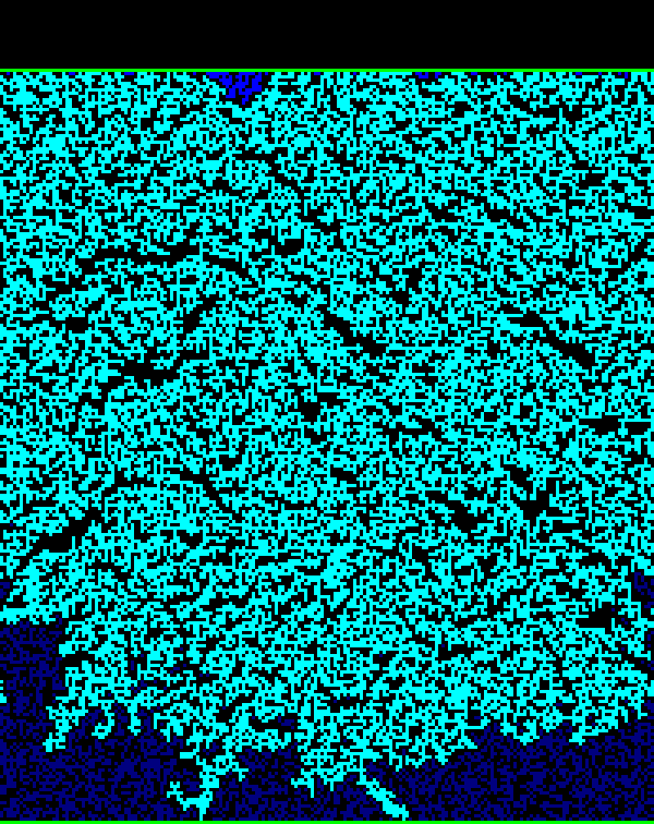
The initial configuration, Fig.1c), is obtained by the following procedure: We start from a lattice gas, where half of the nodes are filled with particles at random positions, Fig.1a). The particles in contact to the upper electrode are shown in light blue. As long as there is no percolation path down to the lower electrode, the upper electrode can push the light blue cluster down by one grid spacing, without changing its structure. When this process is repeated, the cluster of particles in contact with the upper electrode grows (Fig.1b)), until the first percolating path forms, which spans from the upper to the lower electrode (Fig.1c)). It is assumed that the pressure applied to the upper electrode is so weak that a single percolating path is enough to resist further compaction. This is the initial configuration for the simulation of field assisted sintering. The initial inhomogeneity near the lower electrode is greatly reduced after a few simulation time steps as will be shown below.
The simulation proceeds as follows: The current through the system is calculated by a fast algorithm described in ElmNode for fixed voltage between the electrodes. The electrical resistance attributed to the contacts between particles is taken as constant. The Joule heat produced by the current from particle to its neighbor particle during one time step is assumed to be delivered in equal parts to both particles, so that particle receives the heat .
We assume that the the sample is kept at a constant average temperature and the heating compensates the energy loss to the environment at fixed .
| (1) |
For we get the approximation
| (2) |
for the sample temperature.
Particle begins to melt, when the heat exceeds the threshold
| (3) |
needed to raise the local temperature up to the melting point of the nanoparticles, . The temperature dependence of heat capacity close to melting has been neglected, and latent heat needs not be taken into account, since the onset of melting is the appropriate criterion for a particle displacement.
With equation (2) we get the melting criterion
| (4) |
This form is computationally particularly convenient, because the ratio on the left hand side does not change, if the applied voltage is rescaled. This has the advantage that does not need to be kept constant in eq. (2). Any change of can be corrected by an appropriate rescaling of the applied voltage without any effect on the simulation.
A particle with molten surface becomes mobile. It can be squeezed to any free neighboring place as shown in figure 2. This may interrupt the path of the electrical current. If more than one particle have molten they move in random order. Therefore it is possible that a disintegrated current path instantly reappears. After the movement, the particles are reintegrated into the rigid square grid. The grid has a lower mean temperature than the moving particles. Therefore, the reintegration physically corresponds to a recrystallization Schierning2008 . We like to point out, that the model remains applicable, if instead of surface melting a temperature dependent viscosity of the surface layer leads to mobilization of hot particles and their subsequent arrest at a cooler neighboring place.
If the electrical contact between the electrodes was lost because of particle movement, mechanical stability is lost as well. Then the cluster of particles in contact with the upper electrode is pushed down until percolation between the electrodes reappears. Hence the sample becomes more compact.
Calculation of the currents, application of the melt criterion to move hot particles, and finally a compaction of the sample are repeated in every time step. The final configuration is reached, when the melt criterion is nowhere fulfilled any more or the sample became so dense that further compaction is impossible. Remarkably, the only model parameter is . The importance of this key parameter for field assisted sintering has so far not been sufficiently appreciated. Its effect on the final microstructure will be investigated in the following.
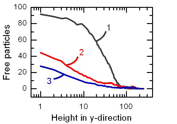
As pointed out above, the initial configurations for our simulations have a zone near the lower electrode that is poorly connected to the upper one (figure 1c). This is a result of the method, by which the configurations were obtained, and will not be found in a real powder. We characterize this inhomogeneity in figure 3, which shows the amount of free particles which have no contact to the upper electrode as function of the height (y-direction) for different stages of the simulation. As one can see, the inhomogeneity is strongly reduced after a short period of about 50 time steps, but it does not vanish completely. We assume that this has only a minor effect on the path formation, because after the first 50 time steps the cluster is connected to the bottom electrode over the width of the whole system, so that the path has enough freedom to form.
We use a length unit of for the grid to compare the simulation pictures with the experimental TEM images of the sample. This length corresponds to the average diameter of the nanoparticles that were used in the experiment.
II.3 Experimental Procedure
Different batches of highly doped silicon nanoparticles with a nominal doping concentration of 5 1020 cm-3 and a mean starting diameter between and were used for field assisted sintering experiments, using a commercial system from FCT (Type HP D40, FCT Systeme Rauenstein, Germany). System and process have been analyzed e.g. in Ref. Vanmeensel . Powders were precompacted and usually they have a density of around 50 % of the value of crystalline silicon after this precompaction. Maximum temperatures were set between and at a heating rate of , but it is known that the measurement technique by pyrometer tends to underestimate the actual temperature slightly Dobedoe . Hold time was kept constant at . A pressure of was applied during the whole sintering process. Care was taken that the sample was electrically isolated from the graphite crucible. This was done by placing the sample within a graphite foil which was coated by boron nitride from the outside. The current was thus lead through the sample and not through the graphite crucible. The process was temperature controlled using a pyrometer focussed on the outer wall of the die wall surface. Current and voltage were set according to the time-temperature program, current being in the range of to , voltage in the range of a few V.
Sintered nanocrystalline samples have about one third of the phosphorus atoms electrically activated, resulting in a charge carrier concentration around and a specific conductivity between and . At room temperature, typical values for the Seebeck coefficient are between – and for the thermal conductivity between – . The high specific conductivity allows to conduct the experiment as described above.
For an investigation of the microstructure, samples were cut into pieces and polished down to a thickness of around . Final thinning to electron-transparency was done using a precision ion polishing system by Gatan inc (PIPS 691). Samples were characterized by transmission electron microscopy and scanning electron microscopy (SEM), the latter using a special adapter for TEM-samples. Microscopes used were a FEI Tecnai ST20 and Jeol JSM 7500F, respectively. The geometric density was obtained by the Archimedes principle by weighing the sample in ethanol and air.
III Results and Discussion
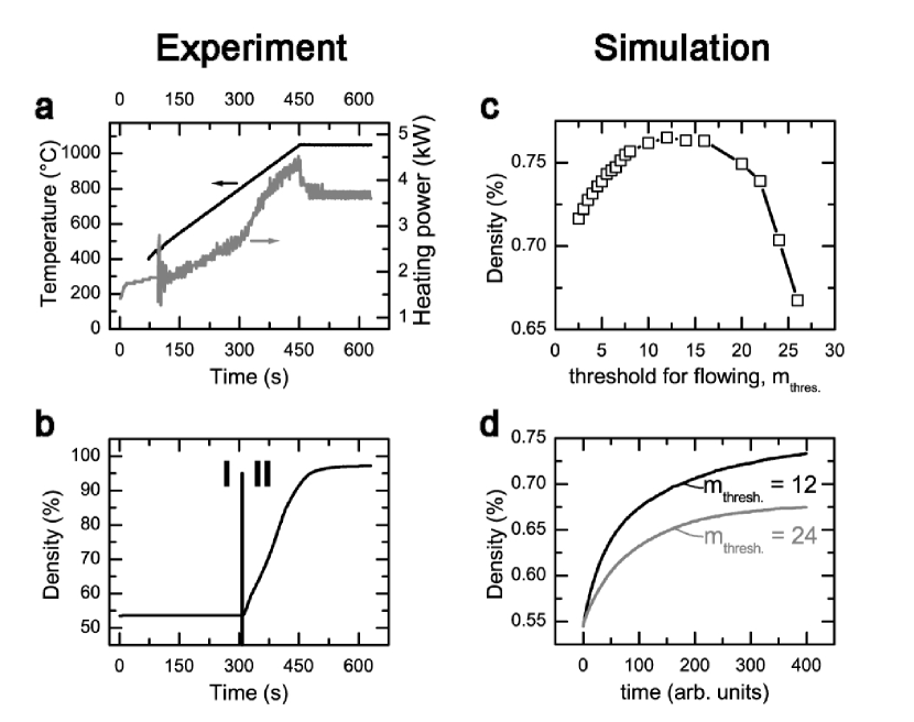
In this section we compare the results of the simulation with microstructural features found in the sintered experimental samples. Figure 4a and 4b show an evaluation of the sintering protocol during densification of a nanocrystalline sample. A constant heating rate is followed by a hold time at . Two different phases can be distinguished:
-
[I]
The first phase is characterized by a constant density of the sample. A rearrangement of particles is highly unlikely as it would directly affect the porosity. Any changes of the electrical properties of the sample in this phase could be caused by thermal and / or electrical breakdown of the oxide layer Xie1 ; Xie2 and local welding at the micro-contacts due to Joule heating as found for larger particlesFalcon .
-
[II]
The second phase is characterized by a steep rise of density. Starting at the temperature of , the density increases from an initial value of 53 % up to 97 % caused by the sintering. This process slows down and the densification saturates eventually. The densification in this phase is captured by the simulation assuming particle reorganization due to local melting.
Around to , first melting events were found for very similar batches of silicon nanoparticles earlier Schierning2008 . Therefore, the temperature window fits well to a fluid phase assisted sintering model assuming partly or even completely molten silicon nanoparticles.
Figure 4d shows the simulation results for the time evolution of the density for two different, constant sample temperatures. They are represented by the parameters and chosen such that the densification begins instantaneously. The density increases and saturates to a value that depends on the sample temperature, in agreement with phase II of the experiment.
Figure 4c) shows the simulated final density as a function of . A low threshold represents a high sample temperature that is close to the threshold temperature for flowing. Accordingly higher thresholds are experimentally realized by lower sintering temperatures. Obviously, for high enough thresholds, no compaction takes place, in agreement with the low temperature behavior (phase I) of the experiment. Below a certain value of the density starts to increase. Surprisingly, the simulation predicts that the compaction is maximal for a value of . For higher sample temperatures the final density decreases again. Experimentally it has so far only been seen that with increasing sample temperature also the compaction becomes stronger. Perhaps the high temperature behavior cannot be seen in the experiment, because the melting temperature is not uniform due to polydispersity. Another reason might be that coordinated movement of particles was not considered in the simulation, therefore a real material has more possibilities to close pores.
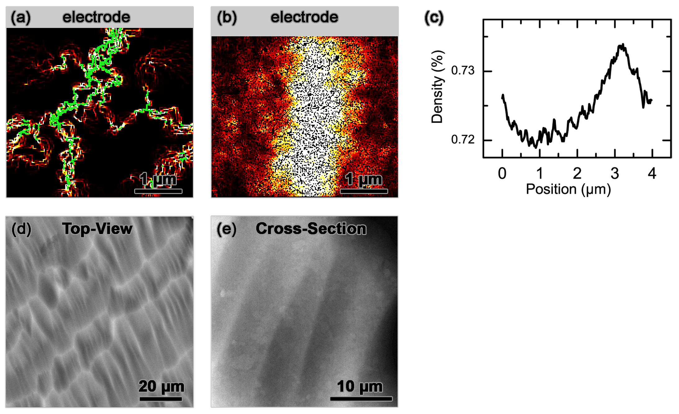
The mechanism underlying the nonmonotonic temperature dependence of the final density is the following: Let us consider cross sections of the simulated square grid parallel to the electrodes. Most heat is deposited in the cross section, which contains the least bonds, because this is the bottleneck of the current. For large , selectively bonds in this bottleneck melt until percolation between the electrodes is disrupted and the sample comptifies. This continues until the fluctuations in become too weak so that the threshold is no longer reached. Lowering makes it easier for compacted samples to still reach the threshold. However, this also widens the molten region, which no longer is restricted to the bottlenecks. This can be seen in Figure 5a), where basically a whole current path melts. The corresponding particle displacement then amounts to a lateral diffusion of the percolating path rather than its disruption. Hence compaction is hindered. This explanation is supported by Figure 5b), where the accumulated heat is color coded to illustrate the diffusion of the path.
While the development of the density seems to support our model, the change of the electrical properties of the sample during the ongoing FAST-process cannot be captured by our simulation. A possible reason is that the moderate heating in phase I has not been included in the simulation. Within this phase, the percolation paths are not expected to disintegrate and fluctuate, as disintegration would be accompanied by a rearrangement of the powder network and thus a decrease of porosity which is not observed. Instead, existing paths ’burn’ into the sample. Contact resistances within those paths may be optimized by breakthrough of the native oxide layer and by local welding. This optimization creates initial conditions for phase II which cannot be mimicked by constant contact resistances between the particles as we have assumed within the simulation. It can be concluded that the simulation so far qualitatively captures the compaction of the field assisted sintering of the highly doped silicon nanoparticles, but fails to model the resistivity decay and increase, because of the constant contact resistance.
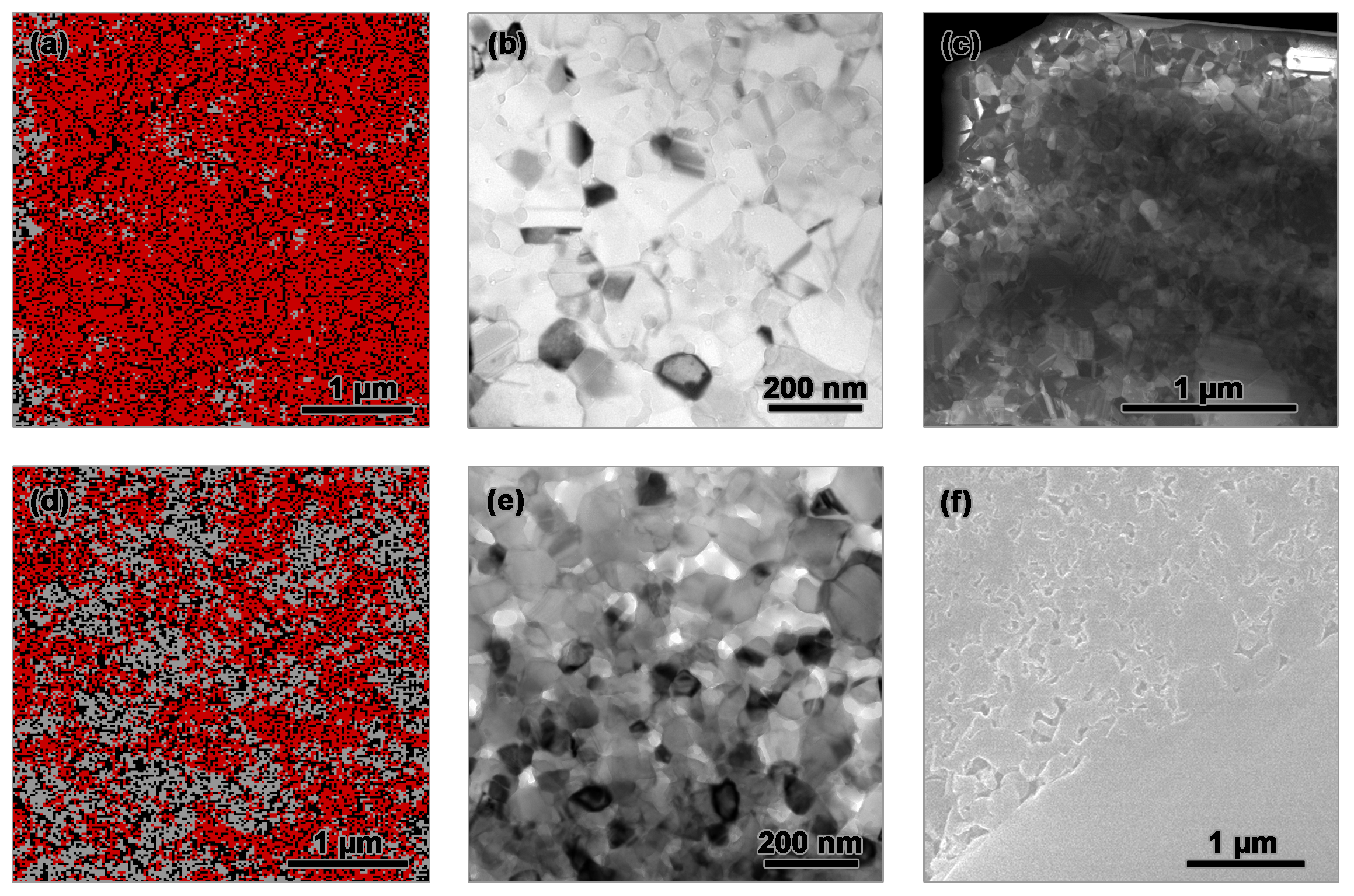
In the following paragraphs, we will analyze the microstructures obtained in field assisted samples. We used the contrast of backscattered electrons in SEM to make a fluctuation of the sample’s density visible (figure 5c and d), assuming that the atomic weight does not show a fluctuation111Note that charging effects can also be excluded as origin of the observed contrast because of the high doping level of the sample.. Obviously, there are paths within the nanosilicon sample which have a higher density than the surrounding matrix, appearing at a micrometer length scale. In top view (figure 5 c) a honeycomb like structure is found. In the crosssection linear paths are found, which are very similar to the simulated heat pattern (figure 5 b). Indeed, in the simulation a weak density increase correlated to this heat pattern has been observed, Figure 5 c). Such patterns are found regularly in nanosilicon samples produced in our laboratory. We conclude that these regions of higher density have their origin in the accumulated heat delivery (figure 5b) produced by the electrical current which have ‘burned’ into the material. This accumulated heating over several time steps leads to a higher sintering activity of the hot regions and therefore to a higher local density.
As a result, the simulation has proven to be in qualitative agreement with experiment, as far as the developing microstructure is concerned: Accumulated heat fluctuations are correctly given by the model and found as density fluctuations in the experiment.
In the following, the parameters of the simulation are varied and compared with experimental investigations. Therefore, the final microstructure of the simulation and the experiment are compared in figure 6. Two threshold-values have been chosen, and , to represent a medium sintering temperature (close to optimal compaction) and a low one, respectively. The medium sintering temperature resulted in a relatively homogeneous sample, both in simulation (figure 6a) and experiment (figure 6b and c). Figure 6c shows a nanosilicon which was sintered at in transmission. The nanocrystalline structure is preserved despite of the density fluctuations due to the current paths as discussed above.
For the low sintering temperature, a different microstructure is expected according to the simulation. Regions which have been molten and regions which were not heated sufficiently are found adjacent to each other and seem to cluster as seen in figure 6d. This is found by a SEM analysis of the accordingly sintered nanosilicon. On a scale of micrometer, very well-sintered as well as bad-sintered regions have formed (figure 6f).
The reason for this may be attributed to the temperature gradients created within the sample. If we assume that the viscous flow of the particle physically always starts at the same threshold temperature (e.g. the melting temperature of the nanoparticles), a low sintering temperature (or high ) means that the temperature variation within the sample is higher because the mean temperature is lower. This will necessarily create inhomogeneities. Note, that these inhomogeneities cannot be reduced by longer sintering times, nor will the density be increased considerably. The well conducting paths have burned into the sample after a short time. The bad-sintered regions will not carry the current to the same amount as the well-sintered regions. Thus, longer sintering times may even result in more extreme inhomogeneities. It can be concluded: If the mechanism of densification is viscous flow, homogeneous samples can only be obtained by choosing the sintering temperature close to the threshold temperature of the viscous flowing.
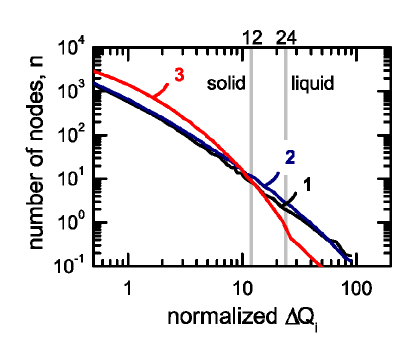
Figure 7 shows a detailed analysis of the temperature distribution (number of nodes at heat ) during the simulated sintering for and . It can be seen that the temperature distribution for remains very close to the initial configuration. Opposing, the distribution changes during the process for . More nodes with lower are found and less particles become mobile during each time step. What does this mean for field assisted sintering? There are only few hot spots created during the sintering if the mean temperature is considerably lower than the threshold for flowing (). At these hot spots, the microstructure will be reorganized only very locally, leading to well-sintered areas which in turn will carry the current afterwards.
For a homogeneously sintered sample, it is important that current paths not only form, but disintegrate again. If the mean temperature during the experiment is close to the threshold for flowing (), many particles become mobile in each time step. Initially conducting current paths will thus be destroyed by the movement of the flowing particles. That is good for the formation of a homogeneous microstructure. Of course, if a nanocrystalline material is intended, the temperature profile has to be well balanced: Too many flowing particles will lead to an unwanted coarsening.
IV Conclusion
Concluding, we used a network model to simulate the field assisted sintering of highly doped silicon nanopowder and compared the simulated results with experimental data. The evolution of density during the sintering process qualitatively matched. We found a good agreement between experiment and simulation with respect to the local temperature distribution which is displayed as density fluctuation in the microstructure of densely sintered nanocrystalline silicon. So we captured some of the main aspects of the FAST process with our simulation approach. As a consequence, some information can be extracted as a guide for sintering dense, homogeneous bulk applying field assisted liquid phase sintering: After a very fast sintering phase in which the densification is observed, the density saturates. Longer hold times, especially at temperatures considerably below the threshold for flowing, will not lead to a further densification but rather increase the microstructural inhomogeneities within the sample. For the developing microstructure, short sintering times at elevated temperatures — i.e. a temperature close to the threshold for flowing — result in best homogeneity combined with high density.
V Acknowledgments
Financial support by the German Research Foundation (DFG) within the Priority Program on nanoscaled thermoelectric materials, SPP 1386, and within the Collaborative Research Center on nanoparticles from the gas phase SFB 445, is gratefully acknowledged. Financial support by the European Union and the Ministry of Economic Affairs and Energy of the State of North Rhine-Westphalia in Germany in the frame of an Objective 2 Programme (European Regional Development,ERDF) and a Young Investigator Grant is gratefully acknowledged. We thank M. Farle, department of experimental physics, for the possibility to use the microscopy facilities.
References
- [1] A. S. Arico, P. Bruce, B. Scrosati, J.-M. Tarascon, and W. van Schalkwijk. Nanostructured materials for advanced energy conversion and storage devices. Nature Materials, 4(5):366–377, 2005.
- [2] G. Chen, M. S. Dresselhaus, G. Dresselhaus, J.-P. Fleurial, and T. Caillat. Recent developments in thermoelectric materials. nternational Materials Reviews, 48(1):45–66, 2003.
- [3] G. J. Snyder and E. S. Toberer. Complex thermoelectric materials. Nature Materials, 7(2):105–114, 2008.
- [4] I. W. Chen and X. H. Wang. Sintering dense nanocrystalline ceramics without final-stage grain growth. Nature, 404(6774):168–171, 2000.
- [5] Z. A. Munir, U. Anselmi-Tamburini, and M. Ohyanagi. The effect of electric field and pressure on the synthesis and consolidation of materials: A review of the spark plasma sintering method. J. Mat. Sci., 41(3):763–777, 2006.
- [6] M. Yoshimura, T. Ohji, M. Sando, and K. Niihara. Rapid rate sintering of nano-grained zro2-based composites using pulsed electric sintering method. Journal of Materials Science Letters, 17:1389–1391, 1988.
- [7] K. Vanmeensel, A. Laptev, J. Hennicke, J. Vleugels, and O. Van der Biest. Modelling of the temperature distribution during field assisted sintering. Acta Materials, 53:4379–4388, 2005.
- [8] R. S. Dobedoe, G. D. West, and M. H. Lewis. Spark plasma sintering of ceramics: understanding temperature distribution enables more realistic comparison with conventional processing. Advances in Applied Ceramics, 104(3):110–116, 2005.
- [9] M. Suganuma, Y. Kitagawa, S. Wada, and N. Murayama. Pulsed electric current sintering of silicon nitride. Journal of the American Ceramic Society, 86(3):387–394, 2003.
- [10] J. R. Groza, M. Garcia, and J. A. Schneider. Surface effects in field-assisted sintering. J. Mat. Res., 16(1):286–292, 2000.
- [11] J. R. Groza. Sintering of nanocrystalline powders. International Journal of Powder Metallurgy, 35(7):59–66, 1999.
- [12] S. K. Bux, R. G. Blair, P. K. Gogna, H. Lee, G. Chen, M.d S. Dresselhaus, R. B. Kaner, and J.-P. Fleurial. Nanostructured bulk silicon as an effective thermoelectric material. Advanced Functional Materials, 19(15):2445–2452, 2009.
- [13] G. Schierning, T. Claudio, R. Theissmann, N. Stein, N. Petermann, A. Becker, J. Denker, H. Wiggers, R. P. Hermann, and R. Schmechel. Nanocrystalline silicon compacted by spark-plasma sintering: Microstructure and thermoelectric properties. Materials Research Society Proceedings, accepted, 2010.
- [14] G. Joshi, H. , Lee, Y. , Lan, X.and Zhu G. , Wang, D. , Wang, R. W. , Gould, D. C. , Cuff, M. Y. , Tang, M. S. , Dresselhaus, G. , Chen, and Z. , Ren. Enhanced thermoelectric figure-of-merit in nanostructured p-type silicon germanium bulk alloys. Nano Letters, 8(12):4670–4674, 2008.
- [15] G. Schierning, R. Theissmann, H. Wiggers, D. Sudfeld, A. Ebbers, D. Franke, V. T. Witusiewicz, and M. Apel. Microcrystalline silicon formation by silicon nanoparticles. J. Appl. Phys., 103(8):084305–6, April 2008.
- [16] Sándor Fazekas Henning Arendt Knudsen. Robust algorithm for random resistor networks using hierarchical domain structure. Journal of Computational Physics, (211):700–718, 2006.
- [17] G. Xie, O. Ohashi, N. Yamaguche, M. Song, K. Mitsuishi, K. Furuya, and T. Noda. Behavior of oxide film at interface between particles of al-mg alloy powder compacts prepared by pulse electric sintering. Japanese Journal of Applied Physics, 42:4725–4728, 2003.
- [18] G. Xie, O. Ohashi, M. Song, K. Furuya, and T. Noda. Behavior of oxide film at the interface between particles in sintered al powders by pulse electric-current sintering. Metallurgical and Material Transactions, 34A:699–703, 2003.
- [19] B. Castaing E. Falcon. Electrical properties of granular matter: from ”branly effect” to intermittency. Powder and Grains, 1:323–327, 2005.
- [20] Note that charging effects can also be excluded as origin of the observed contrast because of the high doping level of the sample.
Figures
a b
b c
c