∎
Tel.: +91-33-24366003
Fax: +91-33-24622153 Ext. 28
22email: tilak@csp.res.in; anuj@csp.res.in; dipak@csp.res.in (: Posted at ICSP by Space Science Division, ISRO Head Quarters, Bangalore, India) 33institutetext: J. P. Malkar, A. R. Rao, M. K. Hingar, V. P. Madhav, 44institutetext: Tata Institute of Fundamental Research, Homi Bhaba Road, Colaba, Mumbai 400 005, India
55institutetext: S. Sreekumar 66institutetext: Vikram Sarabhai Space Centre, VRC, Thiruvanthapuram 695 022, India
77institutetext: S. K. Chakrabarti 88institutetext: S.N. Bose National Centre for Basic Sciences, JD Block, Salt Lake, Kolkata 700 097, India
(Also at Indian Centre for Space Physics, 43 Chalantika, Garia Station Rd., Kolkata 700 084.)
Tel.: +91-33-23355706
Fax: +91-33-23353477
88email: chakraba@bose.res.in
Instruments of RT-2 Experiment onboard CORONAS-PHOTON and their test and evaluation II: RT-2/CZT payload ††thanks: This work was made possible in part from a grant from Indian Space Research Organization (ISRO). The whole-hearted support from G. Madhavan Nair, Ex-Chairman, ISRO, who initiated the RT-2 project, is gratefully acknowledged.
Abstract
Cadmium Zinc Telluride (CZT) detectors are high sensitivity and high resolution devices for hard X-ray imaging and spectroscopic studies. The new series of CZT detector modules (OMS40G256) manufactured by Orbotech Medical Solutions (OMS), Israel, are used in the RT-2/CZT payload onboard the CORONAS-PHOTON satellite. The CZT detectors, sensitive in the energy range of 20 keV to 150 keV, are used to image solar flares in hard X-rays. Since these modules are essentially manufactured for commercial applications, we have carried out a series of comprehensive tests on these modules so that they can be confidently used in space-borne systems. These tests lead us to select the best three pieces of the ‘Gold’ modules for the RT-2/CZT payload. This paper presents the characterization of CZT modules and the criteria followed for selecting the ones for the RT-2/CZT payload.
The RT-2/CZT payload carries, along with three CZT modules, a high spatial resolution CMOS detector for high resolution imaging of transient X-ray events. Therefore, we discuss the characterization of the CMOS detector as well.
Keywords:
Gamma-ray detectors X- and -ray telescopes and instrumentation Laboratory experiments X-ray imaging Solar flarespacs:
07.85.Fv, 29.40.-n 95.55.Ka 01.50.Pa 87.59.-e 96.60.qe1 Introduction
The RT-2 Experiment onboard the CORONAS-PHOTON satellite (Kotov et al. 2008, Nandi et al. 2009) is a dedicated experiment for hard X-ray study of solar flares. It consists of three main detector payloads, namely RT-2/S, RT-2/G (both NaI(Tl)/CsI(Na) scintillator-Phoswich detectors) and RT-2/CZT (solid-state imaging detector) along with one processing electronics device, RT-2/E. Detailed descriptions of the Phoswich detectors and processing electronic device are given in Debnath et al. (2010) and Sreekumar et al. (2010) and the background simulations of the detectors using GEANT-4 toolkit are presented in Sarkar et al. (2010).
The RT-2/CZT payload consists of two different types of imaging detectors: three CZT (Cadmium Zinc Telluride) detectors and one CMOS (Complementary Metal Oxide Semiconductor) detector, arranged in a configuration of 2 x 2 array. The entire detector assembly (CZT and CMOS) sits below a collimator (32 cm height) with two different types of masking devices, namely Coded Aperture Mask (CAM) and Fresnel Zone Plate (FZP). The payload configuration, simulation and experimental results with the coding devices are discussed in Nandi et al. (2010). Due to the different dimensions of the implemented coding devices, this payload has a Field of View (FOV) from 6′ to 6∘. RT-2/CZT payload is the only imaging device onboard the CORONAS-PHOTON satellite to image solar flares in hard X-rays between keV to keV. The CZT detectors have good spectral resolution but moderate spatial resolution. The CMOS detector is capable of imaging with a high resolution. However, it is a single channel device, and is not capable of generating a spectrum.
RT-2/CZT payload is placed outside the hermetically sealed vessel of the satellite and co-aligned to the Sun pointing axis. In §2 and §3 we present individual detector module testing and selection criteria of CZT and CMOS detectors for the flight use. In §4 we present the test set-up for the payload testing and results at different conditions and in §5, we make concluding remarks.
2 CZT detector testing and selection criteria
Cadmium Zinc Telluride (CZT) is an extrinsic semiconductor X-ray detector with a band gap energy of 1.5 - 2.0 eV and an average atomic number, . Due to the high band gap energy, it can be operated at room temperature. As the atomic number () is high, even a few mm of CZT can absorb hard X-rays efficiently (Knoll 1999). In comparison to other X-ray detectors like scintillation detector and proportional counter, CZT needs a relatively low energy deposition for electron-hole pair formation resulting in a good energy resolution (Kotoch et al. 2008). CZT detectors have other major benefits, for example, it can be pixilated by further dividing the sensitive area with segmented anode into multiple pixels which leads to spectral enhancement due to small pixel effect. The current state of art allows one to develop large area X-ray detectors in the form of a mosaic of CZT pixel devices, making this technology really appealing for use in hard X-ray astronomy.
CZT detectors already have been successfully used in the Swift satellite (Barthelmy et al. 2005) and in recently launched Indian Moon mission Chandrayaan-1 (Vadawale et al. 2009). The same detectors would be used in the forthcoming missions like ASTROSAT, EXIST and Constellation-X. We have used CZT detectors in the RT-2 Experiment for hard X-ray solar flare studies. Three CZT detector modules are placed in RT-2/CZT, one of the main payloads of the RT-2 Experiment onboard CORONAS-PHOTON mission, which was launched successfully from Russia on January 30, 2009.
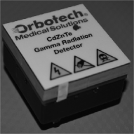
The RT-2 CZT detector modules (OMS40G256) were procured from Orbotech Medical Solutions Ltd., Israel. The detector module (Fig. 1) consists of a 5 mm thick CZT crystal having dimension of cm2. Each module is pixilated to have pixels, where each inner pixel size is mm2, while the edge pixels have a pitch of mm2. The CZT crystal composition (i.e., Cd0.9Zn0.1Te) and growth are achieved using the MHB (Modified horizontal Bridgman) technique (Yadav et al. 2005, Jung et al. 2007, Vadawale et al. 2009). It has a density of gm/cm3. The crystal is N-type conductive having electron as a major charge carrier. The electrodes contacts are made of Indium (Lachish et al. 1999). Cathode is a single mono-electrode, whereas the anode is pixilated to pad size of mm2 with 0.42 mm gap. The CZT detector crystal has been integrated with a multi-channel read-out ASIC’s having 128 channel which are self-triggered and data driven (Yadav et al. 2005, Jung et al. 2007, Vadawale et al. 2009). Its threshold can be externally controlled. These modules can be easily mounted and dismounted from the motherboard through two 20-pin surface mounted connectors in the back side.
OMS40G256 detectors are capable of detecting X-rays of energies ranging from keV. In addition to having all digital interfaces, an optional temperature measurement sensor is integrated with the front end electronics to monitor the temperature of the module, which is useful in monitoring the heat dissipation by the ASICs. The ASIC in each CZT module contains its own pixel map information and inbuilt event storing memory (FIFO) for up to 256 events. The peak position shift of any source spectrum is less than 0.1 keV/∘C. The overall power consumption of a module is about 300 mW, which is about % lower than that of the earlier version of the series of products (Yadav et al. 2005, Jung et al. 2007, Vadawale et al. 2009).
A detailed study of these detectors was carried out for finding its performance, efficiency, etc. in various environmental conditions and to authenticate its use for the space environment.
2.1 Experimental Setup
The System Development Kit (SDK), developed by Orbotech, was used to test our sample detector modules. This system is available from Orbotech commercially and consists of two packages: a detector box and a SDK box. The detector box can accommodate up to 20 detector modules (in a matrix) and it is connected to the SDK box by a 50 pin cable. It gets HV (High Voltage) bias directly from the power supply and the low voltage power through the SDK. The SDK is connected to a computer with an accompanied software which basically allows the control of all ASIC functionalities and data acquisition from the CZT detector modules (Yadav et al. 2005; Vadawale et al. 2009). The SDK software tool saves the spectrum of each pixel data in ASCII files containing the information of event counts per channel.
For the tests at low temperatures, we used a regular laboratory cold chamber which can actively control temperature between -30∘C to 0∘C with the accuracy of 1∘C. We have made the detector box air-tight by covering it with a plastic bag containing two pouches of dried silica gel. The major source of heat dissipation is at the bottom of the CZT detector modules. Therefore, we positioned a temperature probe (thermistor) at the cold finger of the detector module in order to control the detector temperature. The chamber temperature is maintained and varied with respect to this monitoring thermistor temperature.
2.2 Test Procedure
A test procedure was planned on the basis of detector specification provided by OMS Ltd. and desired test environment. The schematic block diagram along with the lab setup of the experiment is shown in Fig. 2.
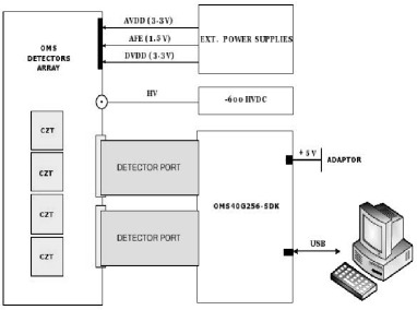
CZT detectors were stored in a low humidity control chamber. This chamber was kept in the clean room for mounting or dismounting of CZT modules from the motherboard (detector board). Radioactive sources Am241 and Cd109 were used for various tests and calibration of CZT detectors. Three separate power supplies were used for the OMS detector test unit to provide two analog (called AVDD and AFE) and one digital (called DVDD) supply voltages along with a common grounding. A high voltage power supply (HVPS) with -V is fed at the top of CZT detector crystal. During this period, we monitored each power supply to verify the nominal power consumption for each detector (Table 1). A dedicated USB port is used for interfacing between the system and SDK unit for data acquisition and to control various parameters of the detector.
On accomplishing all the basic settings required for the test, CZT modules were directly irradiated with two radioactive sources (Am241 and Cd109). Appropriate separation between the sources and detector was kept in such a way that a uniform illumination occurs over the entire detector area. The data were accumulated for intervals of 150 - 1800 seconds as required to obtain a good counting statistics (typically several thousand photons under one energy peak in the spectrum which gives the statistical accuracy of the peak position determination correct to 1%). The average threshold of each CZT module was set at 40 keV in order to avoid low energy noise and to obtain a good spectrum at 59.5 keV and 88.0 keV. It was noticed that heating of detector ASIC creates a large number of noisy pixels in the detector. To prevent this effect, the detector temperature was maintained below 20∘C inside the cold chamber. In order to avoid the moisture condensation, the entire detector unit was kept in airtight container before placing inside the cold chamber. The temperature of detector box was maintained with the help of thermistor placed at the base. Tests were conducted at various temperatures (-20∘C to 20∘C) for characterization (such as, overall performance, energy resolution and stability).
Table 1: Detector power consumption (for one module)
| Voltage ID | Voltage 5% | Typical current | Maximum current |
|---|---|---|---|
| AVDD | +3.3 V | 30 mA | 60 mA |
| AFE | +1.5 V | 20 mA | 40 mA |
| DVDD | +3.3 V | 40 mA | 80 mA |
| HVPS | -600 V | 20 A | 60 A |
2.3 Module screening criteria
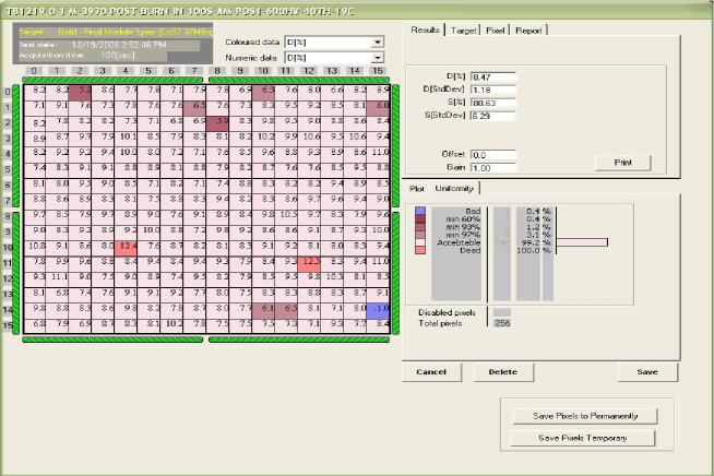
The CZT modules can be operated in command mode (to set thresholds etc.) or event mode when it works as a self-triggered detector and stores pixel number and the energy information (10 bit ADC) in an in-built FIFO, which can be interrogated and from which the data can be collected. The SDK program handles various tasks like communication with CZT digital interface, data acquisition and analysis of the data gathered from CZT detectors. It also provides the performances of each pixel and the various average parameter values of 256 pixels of the selected detector. A single detector (CZT module) can be selected for analysis among the array of detectors inside the detector box using the SDK application. It has also the features like to set and as well as to enable or disable the threshold of detector parameters, view each detector pixel spectrum and events collected by the detector. The information on each pixel can be displayed with appropriate color-coding. For example, Fig. 3 shows a sample display with the color indicating the pixel quality, quantified by various parameters like the percentage energy resolution at FWHM (D[%]); the efficiency (S[%]) defined by the ratio between counts under the photo-peak ( 6.5 of the peak energy) and the total number of counts under the spectrum (integrated from 40 keV to the peak energy + 6.5).
SDK software application was initially used for data acquisition and to quickly analyze the data acquired of the selected module, during the lab test. For a detailed analysis, however, we used the SDK software to store data in event mode files to be read by a tool we have developed using the Interactive Data Language (IDL). This software was specially designed to analyze spectral data with two calibration peaks (e.g. 59.5 keV from Am241 and 88 keV from Cd109). The detector gain (relation between energy and channel) was assumed to be linear in the 20 - 200 keV energy range, as given by specifications, and it was found to be satisfactory during the CZT modules laboratory tests with the rms deviation from a linear fit being 0.5% at 122 keV. Analysis was done by first identifying and removing the unwanted noisy, dead and bad pixels (quantitative descriptions of all types of pixels are given in the next section). Gaussian fittings were made to the two known photo-peaks. The gain (keV/Channel) and offset for individual pixels were calculated using these two photo-peaks. The FWHM derived from the Gaussian fitting is called FWHMFit (fitted). FWHM was also estimated by the number of channels between the two edges of the peak at half maximum and this is called FWHMCal (calculated).
During the analysis, we also calculated the peak efficiency and peak counts. The peak efficiency is defined as the total counts under peak position within 2 level divided by the total counts in the spectrum. We have followed the same procedure for all 30 ‘Gold’ (module with atleast 97% of pixels having average energy resolution of 6.5% @ 122 keV) quality modules that we have selected for initial testing and screening.
2.4 Room Temperature Test
Based on the performance (energy resolution, efficiency, stability, etc.) of individual modules, we selected 8 CZT modules out of 30 modules for the final screening. At room temperature tests, we calculated various parameters (such as peak position, FWHM, Gain, Offset, Energy resolution, peak efficiency etc.) for each of the 256 pixels of all 8 CZT modules.
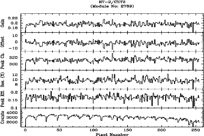
In Fig. 4, we have plotted various parameter of an individual CZT module to demonstrate the pixel-to-pixel variation. There are few disabled pixels during data acquisition (dead or noisy pixel) and pixels with poor response (bad pixels). These pixels are seen either as a dip or high value in comparison to the other pixels in a given detector module. It can be seen from the figure that if we exclude these disqualified pixels (which are less than 4 in a given module), the overall performance is very good. The periodic dip in the total counts variation for all pixels (256) is due to the smaller area of the edge pixels (eg. 16th, 32th, 48th etc.). It is noted that two corner pixels show peak values lower than other pixels, which could be due to the presence of bad pixels in a module, leading to poor energy resolution. The pixel gain (keV/channel) and offset of the entire module appears to remain constant whereas the peak channel number (Pulse Height or PH) has maximum variation of 5. Results shown in Fig. 4 are from one of the CZT module (No. 2789) that is used in space-flight of RT-2/CZT payload.
A standard procedure to evaluate any device is to compare the findings with average outcome from other similar devices. But in case of CZT modules, it is not appropriate to justify all these parameters on the basis of average value calculated by including all pixels of a module, as overall outcome will get affected due to presence of disqualified pixels in a module. Therefore, a methodology was adopted to resolve this complexity of module evaluation by considering the average energy resolution as a prime feature among other parameters and by selecting those pixels which have energy resolutions very close to the best energy resolution pixel. This was achieved using a code (using IDL) that gives an average energy resolution of best 90 pixels and best 75 pixels. As a result the disqualified (hot, dead and bad) pixels were removed automatically from consideration. In addition, the program also provides the information on total number of disqualified pixels along with pixel address. To reduce the impact of these disqualified pixels on the average energy resolution of module, they are filtered out by the program during the calculation. This leads to a better understanding of the module performance and also while evaluating them for the flight purpose.
Similarly, an average value of all defined parameters (Gain, Offset, FWHM etc.) is calculated over best 90 and 75 pixels for all 8 CZT detector modules used in laboratory testing at room temperature. The variation of the parameters of all 8 CZT modules is shown in Fig. 5. The average parameter values of all 8 modules, along with the error bars were calculated and they show a great uniformity. The gain and offset of each module is almost consistently around 0.195 0.010 keV/channel and -2 3 channel whereas the energy resolution given in the term of FWHMCal and FWHMFit is about 9.5 0.5 and 10.5 0.5. In Table 2, we have summarized the energy resolution (at 59.5 keV) informations against pixel wise distribution along with the number of disqualified pixels for all the 8 CZT detector modules.
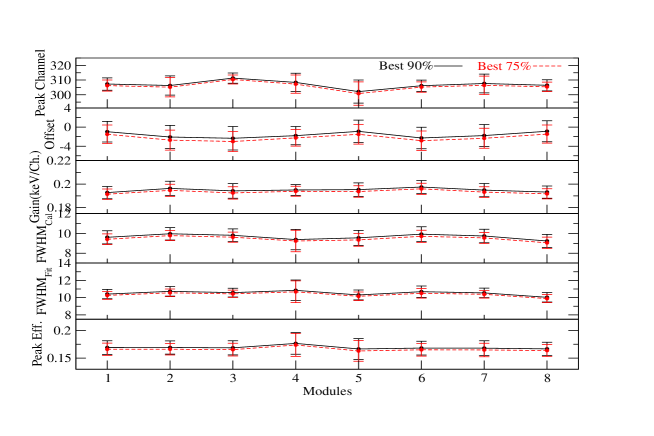
Table 2: Pixel wise energy resolution distribution of the CZT modules
| Sr. | Module | Disqualified | Pixels with energy | Average Energy | ||
| No. | No. | Pixels | resolution @59.5 keV | Resolution | ||
| 10 | 10-14 | Best 90 | Best 75 | |||
| 1 | 2781 | 2 | 54 | 200 | 10.41 0.54 | 10.26 0.45 |
| 2 | 2976 | 2 | 23 | 231 | 10.73 0.56 | 10.56 0.44 |
| 3 | 2789 | 3 | 27 | 226 | 10.58 0.50 | 10.44 0.43 |
| 4 | 2783 | 2 | 15 | 239 | 10.85 1.20 | 10.67 1.26 |
| 5 | 2954 | 5 | 74 | 177 | 10.31 0.58 | 10.15 0.50 |
| 6 | 2957 | 2 | 37 | 217 | 10.69 0.65 | 10.51 0.56 |
| 7 | 2948 | 3 | 41 | 212 | 10.55 0.55 | 10.38 0.44 |
| 8 | 2738 | 5 | 102 | 149 | 10.04 0.55 | 09.88 0.47 |
From Table 2, it is clearly seen that the average energy resolution of the CZT detector modules lies around 10.5 0.5 at 59.5 keV. The performance of modules depends on both the number of disqualified pixels and energy resolutions. There are two types of bad modules: one is defined by a bad spectroscopic performance (the average energy resolutions), while the other type is defined by the presence of large number of disqualified pixels. During the test, the number of dead pixels remains constant with the number of readings taken at different interval of time whereas the hot and bad pixels show variation in their numbers for a given module. There are some hot and bad pixels of the module which can be recovered by optimizing grounding of the entire test setup and by proper cooling arrangement for the test unit (mother board).
During the analysis, we have classified the pixel depending on their spectral behaviors in the following way:
-
•
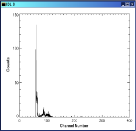
Hot (Noisy) pixel: These pixels are the ones having a very sharp peak or exponentially descending peak (higher count rate) (Fig. 6) compared to the average peak from the source or background. In a module, there are some pixels which are very sensitive to noise either from external sources like inappropriate grounding of the test setup or due to deficiency in heat transfer process which leads to heating of the CZT modules. In Fig. 6, we have shown two spectrum (accumulation time of 150 sec) of different pixels of the same CZT module. In order to show the enhanced feature of noise effect (hot pixel behavior) of two different pixels, we have plotted the spectra in different channel scale (total channel numbers 1024). These noisy pixels can be considerably reduced by taking appropriate action against the origin of noise.
-
•
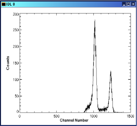
Good pixel: A pixel having a very good efficiency and a Gaussian shaped photo-peak for any radioactive source and uniform background spectrum is defined as a good pixel. Fig. 7 shows the spectrum containing two peaks obtained from the radioactive sources Am241 (59.5 keV) and Cd109 (88.0 keV). The spectrum is obtained for the period of 150 second, similar to the hot pixel accumulation time.
-
•
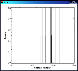
Bad pixel: Pixel having poor sensitivity either due to crystal defect structure (during crystal growth) or improper bonding between crystal and the readout devices (ASIC) of the module. Also, it might be due to mishandling of the device without having proper ESD protection. In comparison to normal (good) pixels, the average count from the source or background are quite less in number (10 counts per 150 sec for photo-peak). An illustration of a bad pixel is shown in Fig. 8.
-
•
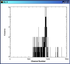
Dead pixel: Pixel with zero output (no count) and having no sensitivity to detect X-rays is said to be a dead pixel. There are many possibilities for a pixel being dead, like crystal defect, weak bonding between crystal and electrodes, mishandling without ESD protection. Unlike the case of a hot (noisy) pixel, there is no chance of recovery of a dead pixel by any means.
2.5 Cooling Effect
At room temperature testing of CZT detector, it was noticed that the modules had an average temperature of 5oC - 6oC higher than the environment temperature, resulting in an increase in leakage current which plays a significant role in the response of each detector module, especially, on the spectroscopic performance. The key features to monitor are performance characteristics of CZT detector and the influence of low temperature operation over the leakage current of the semiconductor.
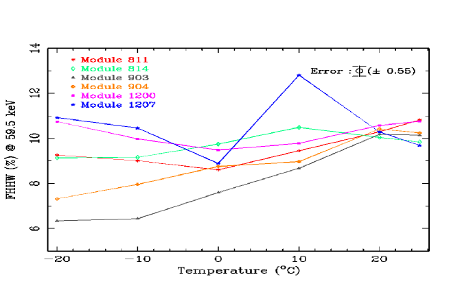
Low temperature (cold) tests were carried out over six CZT modules with the same radioactive sources used for previous measurements. A cold test was performed with the operating temperature ranging from -20∘C to +20∘C and the data was taken when the detector operating temperature become stable within 1∘C. Fig. 9 illustrates the results of cold test in terms of average energy resolutions of each module with respect to the operating temperature, for the 59.5 keV emission peak from Am241 source. These results show clearly that the energy resolution of CZT modules improves with decreasing temperature down to 10∘C and become saturated at 0∘C. Below zero degree centigrade, their spectroscopic behavior change toward energy resolution similar to the ones measured at room temperature. In Fig. 19, we have also shown the result from a flight CZT module, which also shows the same spectroscopic behaviour.


2.6 Life Test
We performed a life test of CZT module to evaluate their response stability and behavior over a long time scale operation. The life test was carried out at room temperature. In Fig. 10 (a,b), we show gain variations of each pixel of two CZT modules monitored for a period of nine days. The gain of these modules remains almost constant over this time scale despite the pixels (every pixel has different gain and characteristics features) getting bad in between for a day and getting back to the normal after sometime which is basically due to temperature gradient effect on the modules. These effects were noticed in both the modules as seen clearly from the sudden rise in the gain of some channels (pixels). This effect is controllable with the help of cooling system to dissipate heat generated by ASIC. Similarly, a sudden rise in pixel count were found due to electromagnetic noise from the surrounding picked by the module, which makes them look like hot pixels. On appropriate grounding of the power supply lines and the body of test setup, these pixels were found to be good.
Further parameters like offset and energy resolution were also under observation during the life test. The aim of life test was to measure the performance, device structural rigidity and stability with signal communication and power consumption are at their norms. On achieving the life test over the modules, there was no such major inconsistency noticed among the above parameters. This indicates that the CZT crystal properties remain invariant with time of detector operation. It could be concluded that the performance of OMS CZT modules (gold) are stable over a long duration run and hence can be used for space flight.
2.7 CZT detectors for space-flight instrument
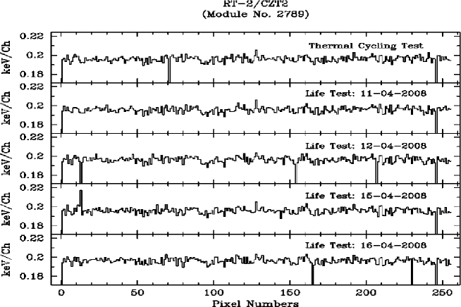
Eight CZT modules (Gold quality) were selected for use in the RT-2/CZT. Out of them, 3 modules were selected for the flight payload on the basis of their performance. To qualify these modules for the space, thermal cycling tests were the first to be carried out for 10 cycles with temperature ranging from -35∘C to 65∘C with the transition rate of 3∘C/min. After carrying out thermal cycling on these modules, there was not any drastic change found in the over all performance of the modules. After going through all the space qualification tests, these modules were subjected to life test which was carried out for 6 days at room temperature.
During the last tests, it was found that a couple of pixels became temporarily noisy. A few pixels were found permanently noisy or dead which were blocked from the respective modules. We found a single pixel which become noisy due to factory defect that is present in every single module, if the threshold is set below 40 keV. In Fig. 11, the results of both thermal cycling test and life test carried out on one of the flight module is plotted, in which gain of each pixel is monitored and compared with respect to each day performance. It was noticed that a uniform pixel gain was seen throughout the tests for all the modules, besides a few disqualified pixels. Similar results were obtained for the remaining two CZT modules for flight use.
3 The CMOS detector
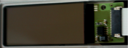
The RadEye1 CMOS (Fig. 12) is a large-area image sensor (procured from Rad-icon Imaging Corporation, USA). It is a complete detection system for high-resolution radiation imaging. The effective area of 24.6 mm x 49.2 mm is made up of a 512 x 1024 array of sensors, where each sensor module contains a two-dimensional photo-diode array with 48 m pixel spacing. Each pixel has its own charge-to-voltage conversion. These CMOS detectors are basically visible imaging photo-diode detectors. But with the help of scintillator, these detectors can be used to detect X-rays and other energetic radiation. A Gd2O2S scintillator screen placed in direct contact with the photo-diode array, converts incident X-ray photons to light, which in turn is detected by the photo-diodes. RadEye1 CMOS imager provides a fully differential high-speed video signal, which is digitized with 12-bit resolution and transmitted to the processing electronics. Its operating temperature range is around 0∘C to 50∘C with dark current (noise) of 4000 electrons/sec at 23∘C (room temperature), which gets approximately double at every 8∘C increase in temperature.
3.1 Test Setup
The implemented CMOS detector is basically a commercial product and as such it has no specific space qualification. Due to its high resolution imaging capability, we have decided to use CMOS as a detector onboard RT-2/CZT payload to perform a fine imaging of hard X-ray solar flares. So, the detector functionality was throughly verified at different temperatures before subjecting it to the space qualification tests.
The detector was enclosed in a plastic bag containing two small pouches of silica gel in order to prevent moisture condensation and with a thermistor mounted on the surface of the detector near to its window for monitoring the temperature. The entire package was made airtight by wrapping the bag with an adhesive tape. This setup was mounted on the thermoelectric cooler to cool the detector to the desired temperature with a variation of 1∘C from the set point. The whole assembly (the package plus thermoelectric cooler) was kept inside a cooled chamber which has the temperature operation range from 0∘C to 25∘C. The radioactive source Am241 was mounted on a fixed position above the CMOS detector plane. The detector is connected to the test electronics (called Shadow-o-Box) using a connector of 15 pins coming out of the sealed package. The Shadow-o-Box is powered with 5V supply from the adapter containing the processing electronics of the detector and it is connected to the input of the grabber card which is implemented in the computer based acquisition system. This card is acting as interface between the detector and system.
3.2 Test procedure
The Shadow-o-Box is powered with 5V supply to make the CMOS detector operational. Using the system based application provided by the vendor, the data is retrieved from the detector to get a raw image of the events. This application needs only once a pixel map file and offset correction information along with exposure time before getting an image from the detector. We acquired the images of the radioactive source by keeping it at different distance above the detector surface with various exposure times (1s, 3s, and 6s). The temperature of the detector was varied from room temperature (23∘C) to 0∘C by step of 8∘C, in order to check its performance and noise characteristic as function of temperatures.
3.3 Results
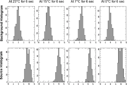
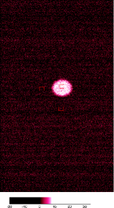
It was observed for sec of image acquisition, that there is a clear and distinct separation between background and source counts distribution. In Fig. 13, we have plotted source and background count distribution at different temperatures. An image of the radioactive source ( keV emission peak) as detected by the CMOS is also shown in the same figure (right panel). On the other hand, for the sec data acquisition, the background variation is almost merged over the source spectrum and the image of the source is too faint and hardly visible. The overall results remain the same during the temperature variation from 23∘C to 0∘C. From the known count rate of the source, we estimate that an energy deposition of about keV per pixel (per sec) is required to clearly distinguish the source from the background, i.e., keV photon will produce approximately the counts of per pixel in comparison to the background counts per pixel.
3.4 CMOS detector for the space-flight payload
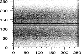
The CMOS detector went through all screening criteria of space qualification process used for the CZT detector modules: stabilization bake, thermal cycling and life test. During the tests, no significant change was found in the performance of CMOS. In Fig. 14, we have plotted the one bit background image (noise) as detected by the CMOS detector. The center dark line of the image is due to the manufacturing split of the entire 512 column into two halves. Detailed analysis on CMOS characterization with Fresnel Zone Plates (FZPs) mask is given in Nandi et al. (2010).
4 Flight model testing of RT-2/CZT payload
RT-2/CZT payload consists of 3 CZT modules and 1 CMOS detector. The overall detector specifications of RT-2/CZT payload are given in Table 3. Note that the geometric area of CMOS is restricted to 25 mm 25 mm and neighboring pixels in a 2 2 matrix are clubbed together to increase the pixel dimension to 100 100 and correspondingly reducing the number of pixels to 256 256.
Table 3: Specifications of RT-2/CZT payload
| Detector type | CZT | Gd2O2S + CMOS |
|---|---|---|
| Thickness (mm) | 5 | 3 |
| Size (mm) | 40 X 40 (3 Numbers) | 25 X 25 |
| Read out (pixel) | 256 x 3 | 256 X 256 |
| Geometric area (cm2) | 48 | 6.3 |
| Energy resolution ( keV) | 10 | NIL |
| Energy range | 20 - 150 keV | 25 - 150 keV |
| Time resolution | 1 s counts and 100 s imaging & spectrum | 100 s imaging |
4.1 RT-2/CZT Electronics
The RT-2/CZT detector assembly contains a Main board (MB) with 3 CZT Modules and a CMOS module. CZT modules are connected on SPI bus which is further connected to Front End Board (FEB). The Main board (MB) is connected to FEB to interface various signals. The other interface of MB is with HV supply, that provides the appropriate bias to CZT modules. The high voltage -600 V bias is provided through a circular connector to each CZT module. The schematic block diagram of RT-2/CZT is shown in Fig. 15.
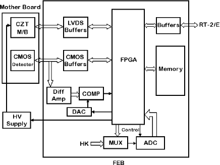
The FEB is the most essential part of the entire electronics. Besides having interfaces with the Motherboard, it has interfaces with the processing unit (RT-2/E). The FEB contains some common interface circuits. One component is the low noise differential amplifier with 50 MHz bandwidths which is employed to amplify the CMOS detector video output. This amplified output is compared with the CMOS threshold given by FPGA to produce one bit image. FPGA is the heart of this board which controls all operations and acquires data from detectors. The SPI interface to CZT module is handled by logic inside FPGA. It is interfaced with CZT modules through LVDS buffers. CZT detector data acquisition and control is done by FPGA through this SPI interface.
The FEB process all the commands needed to configure the CZT modules of operations. The main function of this board is to acquire data from both the detectors and to form spectrum and image in memory. It has a ping-pong memory bank. It sends acquired data to RT-2/E after receiving ‘data-send’ command from RT-2/E. The interface circuitry is necessary to read-out CMOS detector video data which is in differential voltage form. DAC converts a digital threshold value provided by FPGA to analog value. Output of the comparator is considered to be one bit in FPGA for each pixel. Differential signal conditioning offers many advantages over single ended technologies. LVDS signal conditioning centers on 1.25 V with a 350 mV swing and does not depend on power supply voltage. As CZT modules are having LVDS lines, they are interfaced to FPGA in FEB using LVDS buffers.
The RT-2/CZT payload draws raw input power (from satellite power bus during flight) from external supply of 27 Volt. The total power consumption is limited to 7.5 Watt. The input power is converted to 15 V and +5 V with the help of the MDI unit for the required supply of the detector and front-end electronics. A non-controllable high voltage generator (made by PICO) is used to bias (fixed) the CZT detector with -600 Volt. The 5 Volt supply to CMOS is derived from +15 V. The operation of RT-2/CZT payload is completely commandable and controlled by the processing electronic device RT-2/E (Sreekumar et al. 2010).
4.2 RT-2/CZT operational mode
There are two different modes in which RT-2/CZT can be operated: the Event Mode and the Normal Mode. Each event registered by RT-2/CZT is characterized by 2 words. The basic data structure is given below (refer to Sreekumar et al. 2010, for details).
-
•
CZT Event mode data format
The CZT Event mode consists of 32 bits of data words (referred to as bit numbers D0 through D31) with the following configuration:
-
1.
D1 - D0 : Detector ID. 0 to 2 for 3 CZT modules.
-
2.
D9 - D2 : Pixel ID (0 to 255).
-
3.
D19 - D10 : ADC value of the detected signal.
-
4.
D31 - D20 : Time (with a resolution of 0.3 msec).
-
1.
The data stored in memory is sent to RT-2/E unit each second. The maximum numbers of events that can be accumulated are 4032.
For the normal mode, data structure for CZT and CMOS detector is given below:
-
•
CZT Normal mode data format
In the normal mode, CZT spectral and image data are accumulated every second and count rates are accumulated every 10 ms. A total of 5832 words (each word data consists of 16 bits) of memory space are allocated for CZT data.
Image data are accumulated in 4 energy bands or channels (approximately equally spaced in the 20 - 150 keV range, though the channel boundaries can be changed by command) leading to 12 images of 256 pixels (for the 3 modules). Apart from the image, four channel information i.e. counts are stored separately for 10 ms. Therefore, a total of 12 counters (3 modules x 4 channels) are stored for every 10 ms. Spectral data of each module is accumulated in 512 spectral channels.
-
1.
Image block (3072 words): 1 K words per CZT, 4 channel X 256 pixels X 1 word.
-
2.
Spectrum block (1536 words): 512 words per CZT
-
3.
Timing blocks (1200 words): 3 CZT detector X 100 timing words x 4 channels x 1 word (counters in each block will count for 10 ms).
-
4.
Counter block (24 words): 12 counters (2 words each)
-
5.
VCO block (1 word): 2 bytes
-
6.
Special words (8 words): Satellite telemetry word, temperature, Command sent, Data read against command, event number, CMOS line number, Calibration result identification word and Calibration status.
-
1.
-
•
CMOS data format
-
1.
Image block (4096 words): 256 x 256 pixels, 1-bit image.
-
2.
Sum (512 words): Vertical sum (256 words) + Horizontal sum (256 words)
-
1.
4.3 Test and Evaluation of RT-2/CZT payload
Three CZT and one CMOS detector were selected for use in the flight RT-2/CZT payload based on performance obtained during the space screening test and satisfactory results during test and evaluation of the Qualification Model. The Qualification Model is a pre-flight payload and its test results are not summarized in this paper. Only results with the RT-2/CZT Flight payload are discussed in the following sections.
4.4 Test setup
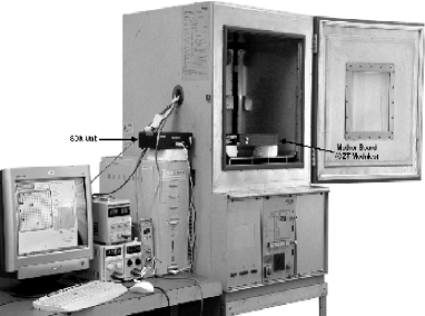
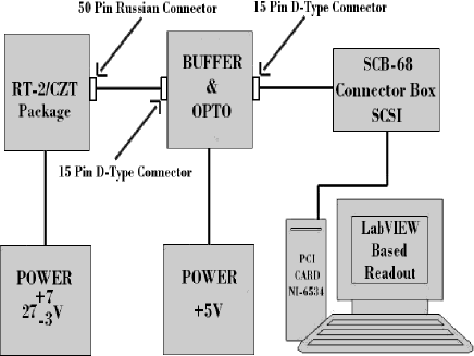
In the flight condition, RT-2/CZT would be fully controlled by RT-2/E. The overall testing of all 3 payloads (RT-2/S, RT-2/G & RT-2/CZT) with RT-2/E and Ground Check-out system is discussed in Sreekumar et al. (2010). We have tested and verified the functionality of RT-2/CZT payload independently, with a computer through an isolator unit, called the OPTO device, SCB-68 connector box and NI data acquisition card (PCI 6534). The OPTO device along with the read-out software were developed using NI LabVIEW platform. The OPTO device is used to isolate the payload electrically from the computer using buffers and opto-isolators. The test setup block diagram for qualifying the RT-2/CZT payload is shown in Fig. 16.
In the laboratory, RT-2/CZT detectors were calibrated with two radioactive sources Am241 (59.5 keV) and Cd109 (88.0 keV). The calibration results, health condition of the payload and overall detector functionality are discussed in the following sections. The operation of RT-2/CZT payload in different modes, channel boundary change of timing data, HV control etc. are commandable. The command structure of RT-2/CZT operation is given in Table 4.
4.5 Flight model test results
CZT detectors are powered with supply voltage of 27 Volt for operation and high voltage supply of -600 Volt for setting the threshold, whereas CMOS is operated with normal 5 Volt supply. The overall power consumption of the payload is 6.75 Watt.
The RT-2/CZT Flight payload contains three CZT detectors with following serial numbers and calibrated energy channel information as given below:
-
•
CZT-1 (Serial No - 2783) - (116 channel corresponds to 20 keV)
-
•
CZT-2 (Serial No - 2789) - (115 channel corresponds to 20 keV)
-
•
CZT-3 (Serial No - 2954) - (114 channel corresponds to 20 keV)
Health informations of RT-2/CZT payload are fed to processing device RT-2/E through ADC. Eight channel ADC output are shown in the table 5.
Table 5: Health informations of RT-2/CZT payload
| Channel No. | Description | Operating voltage level |
|---|---|---|
| 0 | Supply Voltage | 5.0 0.5 V |
| 1 | Thermistor | 1.5 - 5.5 V |
| 2 | GND | 0 V |
| 3 | GND | 0 V |
| 4 | HV OFF/ON | 0.0 V/5.0 V |
| 5 | CZT Supply (DVDD) | 3.6 V |
| 6 | CMOS Supply | 5.0 V |
| 7 | FPGA Supply (VCCA) | 2.5 V |
4.5.1 Spectrum and image validation of CZT modules
All 3 CZT modules (CZT-1, CZT-2, CZT-3) of RT-2/CZT payload have image and spectral information. Apart from the background image and spectrum, we have exposed the modules with a radioactive source Am241 for 20 sec. Each module has detected the emission peak of 59.5 keV along with the calibration source (Co57) peak of 122 keV. The 1024 channels source spectrum and 256 pixels image of all 3 CZT modules are shown in Fig. 17. The measured peak channel number versus the emission peaks energy is given in Table 6.
Table 6: Peak channel informations of CZT modules
| Source | CZT-1 | CZT-2 | CZT-3 |
|---|---|---|---|
| (Energy in keV) | (Channel no.) | (Channel no.) | (Channel no.) |
| Am241 (59.5) | 311.9 | 319.2 | 309.5 |
| Co57 (122.0) | 630.6 | 638.7 | 628.4 |
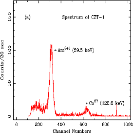
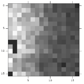
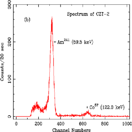
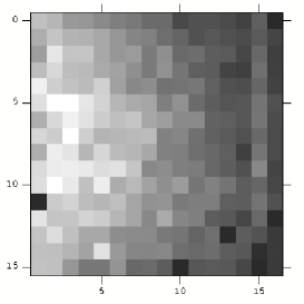
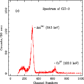
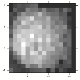
Image of CZT-1 and CZT-2 module show that a few pixels (left side of the module) were illuminated with the source and not all the 256 pixels. This is due to the fact that source is not properly placed. On the other hand, image of CZT-3 is fully illuminated and pattern is in circular form. As per design (see Fig. 2 of Nandi et al. 2010), we have used Coded Aperture Mask (CAM) in CZT-1 and CZT-2 and Fresnel Zone Plate (FZP) in CZT-3 as a coder to cast image on the detector plane (Nandi et al. 2010). It is noted that during testing a few pixels were found to be noisy, which are dark pixels (shown in the image).
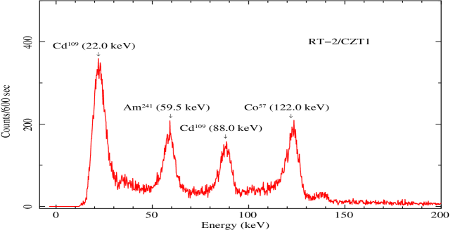
4.5.2 Channel-Energy calibration of 3 CZT modules
Multiple radioactive sources were shinned over all the 3 CZT modules to calibrate the module and to find energy resolution at 10∘C. For calibration we have used three radioactive sources: Am241 (59.5 keV), Cd109 (22.0 keV and 88.0 keV) and Co57 (122.0 keV). The gain calibration is applied to each pixel of a module during the ground testing of the flight payload. This is done by feeding the input of the calibration file generated using IDL code (discussed in section 2.3) from the test data of flight CZT modules. The final spectrum is an integrated one of all the pixels of a CZT module. In Fig. 18, the spectrum of the CZT-1 module with four distinct emission peaks are shown. The corresponding channel and energy values of the emission peaks are used for channel-energy calibration in the energy range of 20 - 150 keV. The same procedure is repeated for the other two modules. We find that the rms deviation from a linear fit of all three modules in the energy range between 20 to 150 keV is 0.5%. From the above analysis, we have calculated the gain (keV/Ch), Offset (keV) and energy resolution at 59.5 keV and 122.0 keV of all 3 CZT modules. The results are summarized in Table 7.
Table 7: Calibration specifications of CZT modules
| Module | Gain | Offset | Energy res. (%) | Energy res. (%) |
|---|---|---|---|---|
| (keV/Ch) | (keV) | (@59.5 keV) | (@122.0 keV) | |
| CZT-1 | 0.201 | 3.43 | 11.02 | 5.74 |
| CZT-2 | 0.199 | 2.90 | 09.89 | 5.28 |
| CZT-3 | 0.204 | 3.21 | 11.99 | 6.32 |
4.5.3 Temperature effect on Pulse Height (PH) & Energy resolution of CZT-2
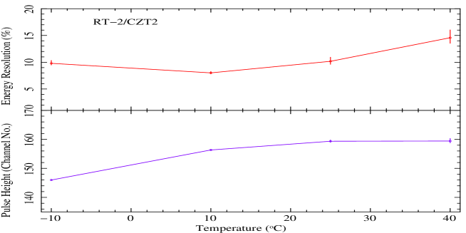
We made a systematic study of Pulse Height (PH) variation of one of the CZT module (CZT-2) with temperature. Payload temperature was varied from -10∘C to 40∘C. Emission peak of Am241 (@59.5 keV) is calibrated as PH and its variation is noted at different temperatures. PH variation with temperature is plotted in Fig. 19 (bottom panel) and it is noted that maximum variation of 6.4% is observed from the normal operating temperature at 10∘C.
In the top panel of Fig. 19, we have plotted the variation of energy resolution (@59.5 keV) at different temperatures. It is noted that the best resolution of 8.5% is achieved in the temperature range of 10∘C to 20∘C and resolution become worse at 40∘C.
Table-4: RT-2/CZT control commands Command Type Command Description Range setting 0x40xx Set range 0 value : xx*2 (8 bit value) 0x41xx Set range 1 value : xx*2 0x42xx Set range 2 value : xx*2 CMOS start line 0x43xx Set the start line of CMOS frame : xx + 256 CMOS upper threshold 0x44xx Set the CMOS threshold : xx*16 CZT constant 0x45xx Set CZT constant, Constant = xx/8 Event mode disable 0x460x Disable CZT from event mode and D0: CZT0, D1: CZT1, D2: CZT2 threshold (0:disable; 1:enable) D4-D3: CZT select for satellite telemetry counts RT-2/CZT HV setting 0x47xx Set HV value for RT-2/CZT from DAC xx=00; HV OFF, xx=01: HV ON One second command 0x4800 Set RT-2/CZT in normal mode 0x4801 Set RT-2/CZT in test mode 0x4803 Set RT-2/CZT in test mode & EEPROM data verify Frame interval 0x49xx Set the time interval in which frames of CMOS are integrated CZT parameters 0x4Axx D5: parity (0) D4: 3.3V (0: ON, 1: OFF) D3: 1.5V (0: ON, 1: OFF) D2: Reset CZT (0: Release, 1: Reset) D1-D0: CZT number (00 - CZT0, 01 - CZT1, 10 - CZT2) CMOS constant 0x4Bxx Set CMOS constant, Constant = xx*16 Memory select 0x4C0x D2: RAM section select D1, D0 : EPROM page select Vertical sum 0x4Dxx Set vertical sum threshold of CMOS, threshold Threshold = xx*8 CMOS control 0x4Exx D7: CMOS control & clock D6 - D0: Clock 20M/(2*(xx+1)) CMOS threshold 0x4Fxx D7: calibration (1: For new threshold) calibration (0: add offset to the present average value of 32 frame Data D6 - D0: threshold for calibration EPROM address set 0x5xx Address : xxx*2 (12 bit value) CZT command mode 0x6000 Set CZT module in command mode CZT event mode 0x6001 Set CZT module in event mode Reset RT-2/CZT 0x6100 Reset RT-2/CZT RT-2/CZT start 0x6101 Start RT-2/CZT EEPROM data 0x62xx Write data in EEPROM EEPROM unlock 0x6303 EEPROM lock 0x6383 CZT commands 0x7xxx 7xxx - 7 00zz xx zz: CZT number xx: command 7 1xxx xx data write 7 0100 00 data read
5 Conclusion
We have presented the test results of several CZT detector modules along with the performance of the 3 selected CZT modules for the RT-2/CZT payload. During the room temperature tests, we observed varied pixels behaviors in terms of response and performance. The numbers of disqualified pixels also vary from module to module. We recognized two different types of bad modules whose behavior can be understood either on the basis of poor CZT crystal or bad ASIC. CZT module functionality appears to vary with temperature. This was revealed by both cold test and also during the space qualification screening procedure. Though the CZT modules can operate at room condition, their best average energy resolution is achieved in the temperature range between 10∘C to 20∘C. Beyond these temperature ranges, some of the pixels may become noisy showing a large variation in counting rate. The average energy resolution which varies with temperature is not uniform for all the modules. This implies that any selection of good CZT detector module for the flight payload shall be based on a trade off between the best average energy resolution and number of disqualified pixels. From the results obtained at 15∘C, we concluded that the number of disqualified pixels should not be more than 5. The results of various flight screening tests conducted over the RT-2/CZT flight payload shows that the overall performance of CZT modules and CMOS detector remains invariant even after going through various environment conditions along with flight electronics. As expected, the flight CZT modules give their best performance at 10∘C ambient temperature. In future, a similar work will be carried out for the development of CZT-Imager payload, ASTROSAT.
On 30th January, 2009, CORONAS-PHOTON has been successfully launched and all the RT-2 instruments, including RT-2/CZT-CMOS, are working with the expected performance. Details of the on-board calibration and data analysis will be published elsewhere.
Acknowledgements.
TBK thanks RT-2/SRF fellowship (ISRO) which supported his research work. The authors are thankful to scientists, engineers and technical staffs from TIFR/ ICSP/ VSSC/ ISRO-HQ for various supports during RT-2 related experiments.References
- (1) Barthelmy, S. D., Barbier, L. M. et al.: The Burst Alert Telescope (BAT) of the SWIFT Midex Mission, Space Science Reviews, 120, 143 (2005)
- (2) Debnath, D., Nandi, A., Rao, A. R., Malkar, J. P., Hingar, M. K., Kotoch, T. B., Sreekumar, S., Madhav, V. P., Chakrabarti, S. K.: Instruments of RT-2 Experiment onboard CORONAS-PHOTON and their test and evaluation I: RT-2/S and RT-2/G Payloads, Exp. Astron. (2010, in press).
- (3) Jung, I., Krawczynski, H., Burger, A., Guo, M., Groza, M.: Detailed studies of pixelated CZT detectors grown with the modified horizontal Bridgman method, Astroparticle Physics, 28, p307 (2007).
- (4) Knoll, G.F.: Radiation Detection and Measurement, Wiley, New York (1999)
- (5) Kotoch, T. B., et. al.: Cadmium Zinc Telluride (CZT) Detectors as an X-ray Imager, Proc. 25th meeting of ASI (2007), BASI, 25Q, 82K (2008)
- (6) Kotov, Yu., Kochemasov, A., Kuzin, S., Kuznetsov, V., Sylwester, J., Yurov, V.,: Set of instruments for solar EUV and soft X-ray monitoring onboard satellite Coronas-Photon. In 37th COSPAR Scientific Assembly, in Montréal, Canada., p.1596 (2008)
- (7) Lachish, U.: CdTe and CdZnTe semiconductor gamma detectors equipped with ohmic contacts, Nucl. Instr. and Methods, Vol 436, 146 (1999)
- (8) Nandi, A., Rao, A. R., Chakrabarti, S. K. et. al.: Indian Payloads (RT-2 Experiment) onboard CORONAS-PHOTON Mission. In Proc. of International Conference on Space Technology, Greece, G. Lampropoulos and M. Petrou (Eds.) (2009) (arXiv:0912.4126)
- (9) Nandi, A., Palit, S., Debnath, D., Chakrabarti, S. K., Kotoch, T. B., Sarkar, R., Yadav, V. K., Girish, V., Rao, A. R., Bhattacharya, D.: Instruments of RT-2 Experiment onboard CORONAS-PHOTON and their test and evaluation III: Coded Aperture Mask and Fresnel Zone Plates in RT-2/CZT Payload Exp. Astron. (2010, in press).
- (10) Sarkar, R., Mandal, S., Debnath, D., Kotoch, T. B., Nandi, A., Rao, A. R., Chakrabarti, S. K.: Instruments of RT-2 Experiment onboard CORONAS-PHOTON and their test and evaluation IV: Background Simulations using GEANT-4 Toolkit, Exp. Astron. (2010, in press).
- (11) Sreekumar, S., Vinod, P., Samuel, E., Malkar, J. P., Rao, A. R., Hingar, M. K., Madhav, V. P., Debnath, D., Kotoch, T. B., Nandi, A., Begum, S. S., Chakrabarti, S. K.: Instruments of RT-2 Experiment onboard CORONAS-PHOTON and their test and evaluation V: onboard software, data Structure, telemetry and telecommand, Exp. Astron. (2010, in press).
- (12) Vadawale, S. V. et al.,: Characterization and Selection of CZT detector modules for HEX experiment onboard Chandrayan-1, Nucl. Instr. and Meth. A, 598, 485 (2009)
- (13) Yadav, J. S., S., Savitri, Malkar, J.P.: Near room temperature X-ray and -ray spectroscopic detectors for future space experiments , Nucl. Instr. and Meth. A 552, 399 (2005)