Theory of optical spin orientation in silicon
Abstract
We theoretically investigate the indirect optical injection of carriers and spins in bulk silicon, using an empirical pseudopotential description of electron states and an adiabatic bond charge model for phonon states. We identify the selection rules, the contribution to the carrier and spin injection in each conduction band valley from each phonon branch and each valence band, and the temperature dependence of these processes. The transition from the heavy hole band to the lowest conduction band dominates the injection due to the large joint density of states. For incident light propagating along the direction, the injection rates and the degree of spin polarization of injected electrons show strong valley anisotropy. The maximum degree of spin polarization is at the injection edge with values at low temperature and at high temperature.
pacs:
72.25.Fe,78.20.-eI Introduction
The optical injection of carriers is a powerful method for the study of the properties of semiconductors, and the optical injection of spins, i.e., optical orientationoptical_orientation , is an important element in the toolkit of the field of spintronics Rev.Mod.Phys._76_323_2004_Zutic ; ActaPhys.Slovaca_57_565_2007_Fabian ; Phys.Rep._493_61_2010_Wu . Most research has been focused on direct optical transitions. There have been fewer studies of indirect optical transitions,in which the excited electron and hole have different wavevectors, and phonon emission or absorption processes are necessary to conserve the total wave vector. In this paper, we consider the indirect optical injection of carriers and spins in bulk silicon.
Macfarlane et al.Phys.Rev._111_1245_1958_Macfarlane first measured the fine structure of the absorption-edge spectrum in intrinsic bulk germanium and silicon in 1958, and identified the phonon-assisted indirect gap absorption branches. Thereafter, these studies were extended to doped siliconProg.Photovolt:Res.Appl._3_189_1995_Green ; Phys.Rev.Lett._70_3659_1993_Suemoto ; Appl.Phys.Lett._93_131916_2008_Mendeleyev ; J.Appl.Phys._61_4923_1987_Saritas ; J.Appl.Phys._50_1491_1979_Weakliem . Theoretically, ElliottPhys.Rev._108_1384_1957_Elliott was the first to study indirect absorption of excitons under the effective mass approximation, and identified the absorption lineshapes at photon energy near and far away from the indirect gap. He found that the lineshapes are not sensitive to exciton effects at high photon energy. The electroabsorption in indirect gap semiconductorPhys.Rev.B_4_4424_1971_Lao ; Phys.Rev.Lett._26_499_1971_Lao and the absorption spectra of multiexciton-impurity complexes Sov.Phys.Usp._24_815_1981_Kulakovskii were also investigated. HartmanPhys.Rev._127_765_1962_Hartman determined the absorption spectra using a parabolic band approximation. DunnPhys.Rev._166_822_1968_Dunn and ChowPhys.Rev._185_1056_1969_Chow ; Phys.Rev._185_1062_1969_Chow used a Green function method to investigate the physical processes in indirect absorption. All these models approximated the matrix elements of the electron-phonon interaction by their band edge values. Later, pseudopotential models Phys.Rev.Lett._48_413_1982_Glembocki ; Phys.Rev.Lett._48_1296_1982_Bednarek ; Phys.Rev.B_42_5714_1990_Li ; Phys.Rev.B_25_1193_1982_Glembocki ; AnnalenderPhysik_504_24_1992_Klenner were employed to calculate the transition matrix elements of the electron-phonon interaction around the band edge. However, a full band structure calculation of the full spectrum of indirect gap absorption is still absent, even with the neglect of the excitonic effects.
Investigations of indirect optical spin injection are less common than those of indirect gap carrier injection. They are also less common than those of direct gap spin injectionPhys.Rev.B_76_205113_2007_Nastos , despite the fact that the first optical orientation experimentPhys.Rev.Lett._20_491_1968_Lampel , performed by Lampel in his study of the nuclear polarization of 29Si in bulk silicon, employed indirect absorption. The degree of spin polarization in such an injection process is sometimes understood as a spin-dependent virtual optical transition combined with a spin-independent phonon absorption or emission processProc.9thInt.Coef.Phys.Semicond._2_1139_1968_Lampel ; PhdThesis_Verhulst_2004 . However, due to spin-orbit coupling the electron states are not pure spin eigenstates, and the effect of the electron-phonon interaction on the indirect gap injection needs to be calculated in detail. While Li and Dery Phys.Rev.Lett._105_037204_2010_Li have recently studied the degree of circular polarization of the luminescence associated with the recombination across the indirect band gap following the electrical injection of spins in silicon, a theoretical investigation of indirect optical spin injection is still absent.
In the present paper, we perform a full band structure calculation of the indirect optical injection of carriers and spins using an empirical pseudopotential model Phys.Rev.B_10_5095_1974_Chelikowsky ; Phys.Rev.B_14_556_1976_Chelikowsky ; Phys.Rev._149_504_1966_Weisz (EPM) for electron states and an adiabatic bond charge model Phys.Rev.B_15_4789_1977_Weber (ABCM) for phonon states. Compared to models and ab initio models, which are widely used for direct gap carrier and spin injection calculation,Phys.Rev.B_76_205113_2007_Nastos ; Phys.Rev.B_81_155215_2010_Rioux the advantage of the EPM is that the electron-phonon interaction in the whole Brillouin zone can be calculated consistently in combination with the ABCM. This approach has been successfully used to describe spin relaxation processes Phys.Rev.Lett._104_016601_2010_Cheng and photoluminescencePhys.Rev.Lett._105_037204_2010_Li in bulk silicon.
We focus on the calculated optical indirect injection coefficients of carriers and spins, identifying the contribution from each valence band and phonon branch. We take the excited electrons and holes as free carriers. Because the electron-hole interaction is nearly spin-independent, to good approximation it should affect the spin injection and the carrier injection rates in the same way, and not affect the degree of spin polarization (DSP) of the injected electrons, which is the ratio of these two quantities. The dependence of the injection coefficients and DSP on photon energy, conduction band valley, and temperature are established. For the injection of carriers, our numerical results agree with the experiments at high photon energy. In the course of our investigations we also discuss in detail a simple but widely used model, in which the values of the transition matrix elements are approximated by their values at the band edge, and we compare its predictions with our calculations.
We organize the paper as follow: We begin with the general formula for indirect carrier and spin injection assisted by phonon emission and absorption in bulk silicon in Sec. II. Then the selection rules that follow from the crystal symmetry are discussed in Sec. III. We introduce the EPM and ABCM models in Sec. IV. Finally we present our results and conclusions in Sec. V and Sec. VI. In an Appendix, we describe an improved adaptive linear analytic tetrahedral integration method (LATM)Phys.Rev.B_49_16223_1994_Blochl ; Phys.Rev.B_76_205113_2007_Nastos that we use to perform the six-fold integration over the Brillouin zone (BZ).
II Model For carrier and spin injection by indirect absorption
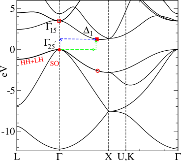
Fig. 1 shows the band structure of silicon in the energy range calculated from the EPM; the details are given in section IV. The lowest four bands are valence bands, of which the upper three are the heavy hole (HH), light hole (LH), and spin split-off (SO) bands. The valence band edge (red dot) is at the point with . All other bands are conduction bands. From the figure, the conduction band edge (red filled square) is at on the symmetry line, and results in six equivalent valleys that can be denoted as , indicating the location of the valley center. The calculated direct band gap at the point is eV, while the indirect band gap is eV. When the photon energy satisfies , optical injection occurs only across the indirect gap. Because the excited electron and hole have different wave vectors, the transition must be assisted by phonon emission or absorption. The green and blue lines show two possible indirect gap transitions between the valence and conduction band edges. The red hollow square and circle indicate possible intermediate states.
For an electric field , the carrier and spin injection rates in silicon can be generally written as
| (1) |
Here and are the injection coefficients for carriers and spins, respectively, at temperature . The superscript Roman characters indicate Cartesian coordinates, and repeated superscripts are to be summed over.
Using Fermi’s Golden Rule, we find the injection coefficient and to be of the form
| (2) |
with
| (3) | |||||
where
| (4) |
Here is the valley index; () is the conduction(valence) band index without including spin; () is the electron (hole) wave vector, where means the summation is over the valley; () give the energy spectra of conduction (valence) bands; gives the phonon energy at wave vector and mode (longitudinal optical (LO) and acoustic (LA), and transverse optical (TO) and acoustic (TA) branches); and , where is the equilibrium phonon number. The operator in Eq. (4) stands for the identity operator in the carrier injection calculation, and the component of the spin operator in the spin injection calculation. The indirect optical transition matrix elements are
| (5) |
in which , , , and are full band indexes, with being the spin indexes; is the electron energy at band and wave vector , and is defined by . The velocity matrix elements are given by , with the velocity operator and the unperturbed electron Hamiltonian ; are matrix elements of the electron-phonon interaction , which is written as , with being the phonon annihilation operator for wavevector and mode .
We now turn to the symmetry properties of . Though bulk silicon has symmetry, each conduction-band valley only has symmetrypeteryu . Therefore each only has symmetry, since the summation over is limited to in the valley. The summation of Eq. (3) can be rewritten as
| (6) | |||||
where
| (7) |
The prime indicates the summation is only over the irreducible wedge of the Brillouin zone, are the symmetry operations in that keep the valley unchanged, while are the symmetry operations in . For each process , the symmetry properties of the tensor with components are the same as those of the tensor with components . Therefore, in the valley, the form a second rank tensor with only two nonzero independent components,
| (8) |
Similarly, the form a third rank pseudotensor with only two nonzero independent components,
| (9) |
where , and are real numbers, and is also a real number because of inversion and time reversal symmetry in bulk silicon. The injection coefficients in other valleys can be obtained by properly rotating the valley to the corresponding valley. The total injection coefficients
| (10) |
have higher symmetry, and the nonzero components satisfy
All quantities keep the identified symmetry properties on summation of one or several subscripts in .
III Transitions at the band edge
The values of the matrix elements at the band edge, , provide insight into the importance of each injection process. For the indirect gap injection in silicon, the conduction band edge in the valley is at , while the valence band edge is at the point, . In analyzing transitions near the band edge, we can use the following two approximations: i) the values of the transition matrix elements [Eq. (4)] are taken at their band edge values, and ii) the values of the wave vector, the energy, and the phonon number of the phonons involved are all taken at their band edge values. Under these approximations, Eq. (6) becomes
| (11) |
with
| (12) | |||||
| (13) |
Here indicates the phonon branches (TA, TO, LA, LO), is the joint density of states (JDOS) for indirect gap injection, gives the symmetrized transition matrix elements at the band edge, and indicates summation over all modes in the branch. Under the parabolic band approximationPhys.Rev._127_765_1962_Hartman , the JDOS is
| (14) |
We now turn to . Because the HH and LH bands are degenerate at the point and their wave functions are not uniquely determined, unambiguous values of and for the HH and LH bands separately do not exist at the band edge. But this is not a problem for , due to the summation over all symmetry operations. To show this clearly, we indicate all intermediate states in the transition matrix elements implicitly by writing
| (15) |
with the operator
| (16) | |||||
Substituting Eq. (15) into Eq. (4), it is easy to find that the expression for includes a summation , which equals when is the HH or LH band. So are unambiguous, and give the same value for both the HH and LH bands. This conclusion mirrors a similar one in the study of injection across the direct gapPhys.Rev.B_76_205113_2007_Nastos . In the following, we focus on selection rules for . Li and Dery Phys.Rev.Lett._105_037204_2010_Li also discussed the selection rules in the context of luminescence by considering only the lowest conduction band and the highest valence band as the intermediate states; they also assume equal amplitudes for the two interference processes shown in Fig. 1. Here we give a general discussion using Eq. (15), without relying on the properties of the intermediate states.
Without spin-orbit coupling, the valence band states at the point transform according to the representation (with basis functions that transform as , which are labelled as here)Phys.Rev.B_76_205113_2007_Nastos . We first consider the electron states that lie in the valley, in which the conduction band edge state transforms according to the representation (basis function )peteryu . The phonon states involved transform according to the representation (basis function ) for the LA phonon mode, (basis function ) for the LO phonon mode and (basis functions ) for the TA/TO phonon modes;peteryu has the same symmetry properties as the branch phonon polarization vector. The velocity transforms according to the representation . All nonzero components of the vector are listed in Table 1 for the different valence bands and phonon modes. In Li and Dery’s approximations, and because the two transition processes summed are of equal magnitude, and vanishes due to their limitation of the intermediate states. In contrast, we keep all nonzero terms in our treatment, and give their values in Sec. IV.
| phonon mode | ||||
|---|---|---|---|---|
| TA/TO | LA | LO | ||
| 0 | ||||
| 0 | ||||
| 0 | ||||
With spin-orbit coupling, the valence bands at the point are split into HH (), LH () and SO () bands with the following states:
| (17) |
The SO band at the point is lower than the degenerate HH and LH bands by meV. At the conduction band edge, the states can be approximately written as and due to the very small spin mixing. The transition matrix elements between these states with spin-orbit coupling can be obtained by linearly combining the terms in Table 1.
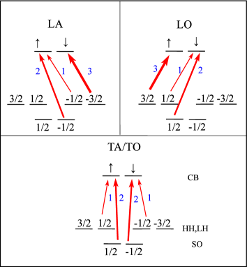
For light, , we show in Fig. 2 the possible optical transitions from the valence bands to the valley of the conduction band. Here the spin quantization directions of both electrons and holes are chosen along the direction. It is obvious that the phonon states play a key role in these transitions. For transitions from HH and LH bands, the LA and LO phonon-assisted processes inject spin polarization along the and directions, respectively, with a DSP of , yet there is no spin polarization from the TA/TO phonon-assisted processes. Despite its spin independence, the electron-phonon interaction still affects the selection rules for spin injection since all states involved are not pure spin states due to spin-orbit coupling. Therefore, it is not adequate to treat the indirect transitions as a spin dependent virtual optical transition combined with a phonon emission or absorption process that does not affect the spinProc.9thInt.Coef.Phys.Semicond._2_1139_1968_Lampel ; PhdThesis_Verhulst_2004 .
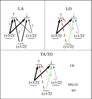
Now we look at the transitions to the electron states in the valley. The possible optical transitions are complicated, and are shown in Fig. 3. To simplify the diagram, we choose the quantization axis of the hole states along the direction, and that of the electron states along the direction. Here the LO and TA/TO phonons can play a role in spin injection, but the LA phonon cannot. Thus there is strong valley anisotropy in the injection of spins. In Li and Dery’s approximations, the TA/TO phonon-assisted processes give a DSP of from the HH and LH bands, and the LO phonon-assisted process gives no spin polarization. In our more detailed analysis, we cannot simply identify a DSP for each process, as some of these processes are determined by more than one nonzero parameter. We discuss the actual values of these at the end of section IV.
Because the band edge transitions strongly depend on the choice of the electron and hole states, it is constructive to give the nonzero components of . They can be specified by giving the values of , in terms of which are found following the pattern of Eq. (8) and (9). The results are shown in Table 2. In the calculation, we have used the result that the contributions for the HH and LH bands at the point are exactly the same.
| TA/TO | LA | LO | ||
| SO | ||||
| LH,HH | ||||
| SO | ||||
| LH,HH | ||||
From Table 2, we find that some results are similar to those for direct gap injection: The band edge transition magnitudes for carrier injection are the same for each valence band, while the ones for spin injection are only identical for HH and LH bands, and satisfy
| (18) |
The vanishing sum does not mean that the spin polarization becomes zero when the laser pulse is wide enough to involve all valence bands, because the densities of states for different valence bands are different. However, as the photon energy increases, the optical transition occurs away from the band edge, where the involved electron and hole states are superpositions of the band edge states of all valence bands. As a consequence of Eq. (18), important band mixing leads to a small DSP.
IV Model for Electron states and phonon states
To look at the carrier and spin injection away from the band edge, a full band structure model of the electron and phonon states is necessary. We use the EPMPhys.Rev.B_10_5095_1974_Chelikowsky ; Phys.Rev.B_14_556_1976_Chelikowsky ; Phys.Rev._149_504_1966_Weisz for electron states and the ABCM Phys.Rev.B_15_4789_1977_Weber for phonon states. We describe these now, and give the resulting electron-phonon interaction for indirect gap injection. In the EPM, electrons are described by the pseudo-Hamiltonian,
| (19) |
Here is the momentum operator; is the equilibrium position for the () atom in the primitive cell located at with and , and is the lattice constant; is the atomic empirical pseudopotential, in which and are the local and nonlocal spin independent pseudopotentials, respectivelyPhys.Rev.B_10_5095_1974_Chelikowsky ; Phys.Rev.B_14_556_1976_Chelikowsky , and is a spin dependent contribution Phys.Rev._149_504_1966_Weisz introduced to fit the spin split-off energy at the pointPhys.Rev.Lett._104_016601_2010_Cheng . Eigenstates of are given by the Bloch states , where are plane wave states, is a reciprocal lattice vector, and are coefficients obtained by solving the single-particle Schrödinger equation.
The Fourier transform of the pseudopotential is
| (20) |
For the local pseudopotential taken to be of the form with , we have that depends only on , and we write it as . Chelikowsky and Cohen Phys.Rev.B_10_5095_1974_Chelikowsky ; Phys.Rev.B_14_556_1976_Chelikowsky showed that a suitable electron band structure can be produced by taking the values of only at , 4, and 11 , which lead to the conduction band energy at the point of 1.17 eV. In order to produce the direct band gap , the indirect band gap , and the location of the conduction band edge correctly after including the spin-orbit coupling, we use the following parameters , , , , and eV for , 4, 11, 16, and 19 . The calculated band structure is shown in Fig. 1. The calculation is for zero temperature. With increasing temperature, the electron-phonon interaction induces changes at the band edge and shifts the indirect and direct band gapsPhys.Rev.B_31_2163_1985_Lautenschlager ; J.Appl.Phys._51_2634_1980_Mahan ; J.Appl.Phys._45_1846_1974_Bludau ; J.Appl.Phys._79_6943_1996_Alex . For silicon, the shift in the conduction band edge is minor; we absorb it into in the following.
For the phonons, the ABCM is used for calculating the polarization vectors and energies . The calculated band structure fits the experiments wellPhys.Rev.B_15_4789_1977_Weber . The energies of phonons with wave vector , which are involved in the band edge transition, are meV, meV, meV , and meV.
By shifting the atom position from the equilibrium position to , and then expanding the electron Hamiltonian (19) to linear order in , we identify the electron-phonon interaction as . The atomic displacement is usually expanded by the phonon polarization vectors as
| (21) |
with being the mass density of silicon. The transition matrix elements between different electron states are given as
| (22) |
where , .
In calculating the matrix elements of the electron-phonon interaction given in Eq. (22), the values of at all points are necessary, and they are obtained using the natural cubic spline interpolation Phys.Rev.B_48_14276_1993_Rieger on the discrete points given above and two further restrictions: the first is the value ; the second is a cut off at high , , where is a cut-off value. Bednarek and Rössler Phys.Rev.Lett._48_1296_1982_Bednarek showed that the values assumed for and strongly affect the calculated matrix elements of the electron-phonon interaction in Eq. (22). In our calculation, we find that the assumed value of doesn’t significantly affect for , and we set . We show the dependence of indirect absorption on in Table 3 and 4 by taking (denoted as case A) and (case B). Here and are the Fermi wave vector and Fermi energy of the free electron gas appropriate to the valence electron density in silicon.
| TA | TO | LA | LO | |||||||
|---|---|---|---|---|---|---|---|---|---|---|
| A | 0.020 | 0.018 | 0.131 | 1.000 | 0.018 | 0.218 | 0.001 | |||
| B | 0.066 | 0.090 | 0.120 | 1.024 | 0.020 | 0.192 | 0.026 | |||
| valley | valley | total | ||||||||
| TA | 0.0117 | 0 | 0 | 0.019 | 0.100 | |||||
| LA | 0.0122 | 0.006 | 0.00022 | 0.0488 | ||||||
| A | LO | 0.145 | 0.0727 | 0.073 | 0.00473 | 0.583 | 0.164 | |||
| TO | 0.667 | 0.42 | 3.01 | -0.489 | ||||||
| TA | 0.0603 | 0.074 | -25% | |||||||
| LA | 0.0135 | 0 | 0 | |||||||
| B | LO | 0.128 | 0.064 | 50% | 0.072 | 0.023 | 32% | 41% | ||
| TO | 0.682 | 0 | 0 | 0.421 | 3.05 | |||||
For carrier injection, the contributions from the phonon branches other than TA are essentially the same in case A and B, while for spin injection the phonon processes involving TA or LO phonons and electron injection into the valley give contributions that depends strongly on the value of . The DSP for the LO phonon-assisted process is about in case A and in case B. Nevertheless, by far the most important contribution to indirect gap injection comes from the TO phonon-assisted process, which is almost independent of for both carrier and spin injection. In the following, we use the parameters of case A.
Contrary to what was assumed in Li and Dery’s results, our results show that or cannot be well satisfied. But the calculated DSP for TA/TO phonon-assisted processes in the valley is still close to . The value of is reasonably small.
V Calculations
To obtain the injection rates, we can focus only on energies near the band edge and rely on Eq. (11), or numerically evaluate Eq. (6) using the results of a full band structure calculation. Both strategies require a six-dimensional integration over the electron and hole wavevectors ranging within the BZ. In the present work, we vary the photon energy to about 1.5 eV above , which results in an effective integration volume consisting of about 3/8 of the volume of the whole BZ, and a very demanding calculation. Similar to the integration used in the calculation of direct gap injection, the integrand here is composed of an energy conservation term, i.e. the Dirac function, and a transition matrix element term. In a calculation of direct gap injection, the function is evaluated using a LATMPhys.Rev.B_49_16223_1994_Blochl ; Phys.Rev.B_76_205113_2007_Nastos on a very fine grid, and the transition matrix elements are calculated on each grid point. However, this method is not practical in a calculation of indirect gap injection, because the transition matrix elements are too complicated to be evaluated on each point of a fine grid. Instead, we find that we can obtain a converged result by using separate grids for these two terms, adopting a finer grid for the Dirac function and interpolating the transition matrix elements on a rougher grid. The details of this method are in Appendix A.
In our calculation, the valence bands include HH, LH, and SO bands, the conduction bands include the lowest and the first excited conduction bands, and the intermediate states are chosen as the lowest 30 bands to ensure convergence.
The total carrier and spin injection from any pair of valence bands via an emission or absorption process involving a phonon of any branch, as well as the carrier and spin injection into any conduction band valley, are completely determined once the quantities and are specified: The nonvanishing Cartesian tensor components follow from Eqs. (8) and (9), the sum over the different valleys follows from Eq. (10), and the full response tensors follow from Eq. (2); once these are determined the injection rates can be calculated from Eq. (1) for any light polarization. Instead of presenting our calculated results for and below, we present instead
| (23) |
These are the terms that appear in a simple excitation scenario using light, as described in the following section. They correspond to the injection into different valleys via the different processes. Nonetheless, we stress that given the quantities in Eq. (23), we can construct the carrier and spin injection in Eq. (1) for any polarization using Eqs. (8), (9), and (2).
VI Results
In the following, we focus on injection under light. In this case, the six valleys can be divided into two sets: {} and {}. The injection is identical for all the valleys within each set. The carrier and spin injection from the valence band into the conduction band in the valley via a -branch phonon emission () or absorption () are identified by and , respectively, which are given from Eq. (23) as
| (24) |
with . Accordingly, the coefficients
are also used in the following to understand the injection properties. Here TA, LA, LO, TO are the phonon branches; as before, indicates to a sum over all phonon modes in the branch. Similar notation is used for the injection coefficients of spins. We find that the polarization direction of injected spins in each valley is parallel or anti-parallel to the direction. The DSP is defined as
| (25) |
Here indicates the subscripts for are the same as that for and .
VI.1 Carrier injection
VI.1.1 Band edge carrier injection at 4 K
We first study the carrier injection at the band edge at 4 K. For band edge injection, only the transitions between the lowest conduction band and the valence bands need to be considered; the first excited conduction band is ignored due to its small density of states. At this low temperature, only the phonon emission process is important. In Fig. 4 we show the spectra of the total injection rate (black thick solid curve) as well as the injection rates in and valleys (black thick dashed and dot-dashed curves). All injection rates increase with increasing photon energy. These results are consistent with the analytical results in section III, where the injection rates around the band edge are approximately proportional to the JDOS. The difference between the injection rates in the and valleys shows that the injection is valley anisotropic. To understand the contribution from each phonon branch, we plot phonon-resolved injection rates in Fig. 5. We find that each phonon-resolved spectrum has a shape similar to the total. In our calculation, the importance of the phonon-assisted processes are in order of TO LO TA LA, in which the contribution of the LA-assisted process is less than 5%.
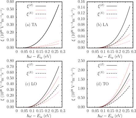
At the band edge, the injection rates can also be obtained from the simplified calculation given by Eq. (11), which can be used to identify how well the selection rules in Table 2 work. The results of the simplified calculation are also plotted in Figs. 4 and 5 as red thin curves. Compared to the full calculation, Fig. 5 shows that these results have smaller values for the TA, LA, and LO branches, and a larger value for the TO branch. The differences are significant for acoustic phonons, and minor for optical phonons. Even for optical phonons, the difference is about 30% at excess photon energy of eV. However, because the errors for the two most important phonon branches, i.e. TO and LO branches, are opposite, the difference in the total injection rates between these two methods is not so great. This difference illustrates not only the variation of the transition matrix elements on and , but also the failure of the simplified formula at high photon energy. Nevertheless, the simplified formula gives the correct qualitative results.
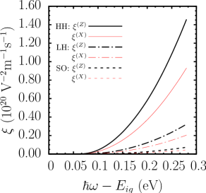
To better understand the details of carrier injection, we also plot the contribution from each valence band to for the TO-assisted process in Fig. 6. There are two important features: First, all injection rates increase with photon energy, which can be understood by the increase of the involved JDOS with photon energy. Second, the HH band gives the greatest contribution to the injection rate, and the SO band gives the smallest. As the transition matrix elements are the same for these three bands at the band edge, the magnitude is determined only by the density of states of each valence band. Similar results are obtained for the other three phonon branches.
VI.1.2 Comparison with experiment at 4 K
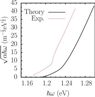
Fig. 7 gives the photon energy dependence of at K. Here is the absorption coefficient, is the refractive index of silicon, is the speed of light, and is the vacuum permittivity. Our result (the solid curve) shows two important features of the indirect gap injection: Near the onset of absorption, for , the TA phonon emission process dominates, then the optical phonons make important contributions for . The separation between these two regions is indicated by the kink in the figure. In each region, the lineshape of is approximately a linear function of , which is consistent with the results in the parabolic band approximation, i.e., Phys.Rev._127_765_1962_Hartman ; Phys.Rev._108_1384_1957_Elliott . With respect to these features, our results match the experimental results very well.
Yet compared to the experiment by Macfarlane et al. Phys.Rev._111_1245_1958_Macfarlane , our result fails to show the correct energy shift and lineshape at the beginning of each region. Both of these features are related to the excitonic effect, which is absent in our calculation. When the excitonic effect is considered, both the bound and continuum exciton states contribute to the absorption, as discussed in detail by Elliott: Phys.Rev._108_1384_1957_Elliott The onset of absorption is shifted to lower energy by the presence of exciton bound states, and modified to give a line shape associated with the first exciton bound state and each phonon branch, with an exciton bind energy meV;J.Appl.Phys._45_1846_1974_Bludau the lineshape of the absorption associated with the exciton continuum states is similar to that calculated without including the electron-hole interaction. Despite all this, in the next we will see that the absorption at high photon energy can still be well described by our model. Even at low photon energy, we expect our model can give a reasonable description of the DSP, because the excitonic effects are to good approximation spin independent.
VI.1.3 Carrier injection at high temperature
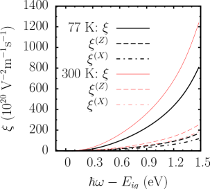
The indirect gap injection rates depend on the phonon number, and thus on the temperature. With increasing temperature, the phonon absorption processes come into play, and the onset of the injection spectrum moves to lower photon energy. The equilibrium phonon numbers at different temperatures are as follows: At 77 K, all phonon numbers can approximately be ignored, so only the emission processes occur. At 300 K, the phonon numbers become for TA, for LA, for LO, and for TO. Because the TA phonon has smaller energy, the absorption induced by the TA phonon-assisted process is the most temperature-sensitive.
In Fig. 8 the spectra of , and are plotted for 77 K (black thick curves) and 300 K (red thin curves). All injection rates increase remarkably with temperature: displays about 50% increase when the excess photon energy is 1.5 eV. Note that the injection rates at 77 K and 4 K are approximately the same. The phonon-resolved absorption spectra at different temperatures are plotted in Fig. 9. The injection rate from each phonon branch increases with temperature, and the increment is most significant for the TA phonon branch. At 300 K, is comparable to ; at low temperature, is less than half of .

VI.1.4 Comparison with experiment at high temperature
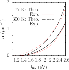
In Fig. 10, we compare our results for the absorption coefficient with experimental resultsSze at and K. Compared to the results near the band edge, the calculations without including excitonic effects fit the experiments better at high photon energy. The difference between theory and experiment at low photon energy can be attributed to excitonic effects and the temperature dependence of the indirect band gap energy, neglected in our calculation which takes that energy as its zero temperature value. Clearly our neglect of excitonic effects and of this gap energy shift has less consequence at higher energies. In the calculation, we use the experimental frequency-dependent refractive index Prog.Photovolt:Res.Appl._3_189_1995_Green . Because of the increase in phonon number, the absorption coefficient at 300 K is remarkably larger than at 77 K.
VI.1.5 Temperature dependence of carrier injection
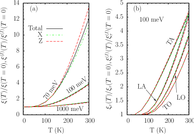
Fig. 11 (a) gives the temperature dependence of the ratio (black solid curves), (green dash-dotted curves), and (red dashed curves) for 70, 100, and 1000 meV. The injection rates increase with temperature for all photon energies, and their slopes decrease with photon energy. When the temperature is lower than 70 K, the injection rates are almost independent of temperature, while they become nearly a linear function of temperature at temperature higher than 200 K. Their slopes depend on the photon energy with larger slopes at lower photon energies. The slopes for the injection in the and valleys are found to be different at low photon energy, with the difference tending to disappear at high photon energy. The temperature dependence of phonon-resolved injection rates for excess photon energy meV are plotted in Fig. 11 (b). The temperature dependence of the phonon-resolved injection rates are similar to the total, but show different slopes for different branches. In order to give an comprehensive understanding of these results, we use the simplified formula for the band edge injection in Eq. (11). At high temperature, the phonon number is approximately , and Eq. (11) for absorption near the band edge can be rewritten as
| (26) |
The linear dependence at high temperature is obvious. The slope is determined by the photon energy, and decreases as the photon energy increases. At photon energy displayed in Fig. 11 (b), however, the dependence of the slope on phonon energy is too complicated to be described by this simple formula.
VI.2 Spin injection
VI.2.1 Band edge spin injection at 4 K
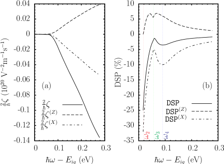
In Fig. 12 (a) we show the spectra of the spin injection rate in the valley (dashed curve) and the valley (dash-dotted curve) as well as the total (solid curve) at 4 K. The spin injection rates increase with photon energy, and show strong valley anisotropy, as do in carrier injection. But the photon energy dependence of the spin injection rates does not follow the quadratic JDOS, but nearly a linear function. This indicates the strong wavevector dependence of given in Eq. (4). The injected spins in the and valleys have opposite polarization direction. Fine structures of spin injection can be found from the DSP spectra given in Fig. 12 (b). The total DSP at the band edge ( meV, corresponding to the TA phonon emission process) is about , while the DSP in the and valleys approximates and . When the photon energy is higher than , the spectra can be divided into three regions: i) with meV (). Here the and the decrease rapidly with increasing energy to a minimum value of and , respectively, while the increases to a maximum value of when the photon energy is slightly smaller than , and then decreases slightly to a local minimum at . ii) with meV. Here the and the increase to a maximum value and , and the first slightly increases and then decreases. iii) . All decrease monotonically to zero. The special photon energy is related to the TO phonon energy given in Sec. IV, the features here are formed by the contributions from different phonon branches, which are plotted in Fig. 13.
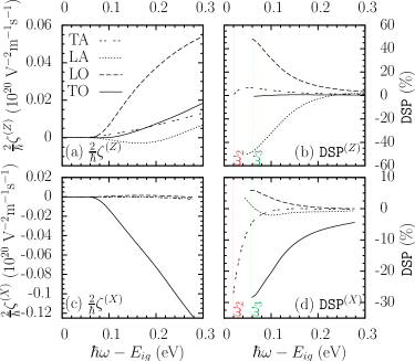
According to the phonon energies, the injection edge energies of different phonon branches are ordered as TA LA LO TO, which is obviously shown in Figs. 13 (b) and (d). For the spin injection in the valley given in Fig. 13 (a), the contributions from all phonon branches are almost of the same order of magnitude, even including the LA phonon branch, which gives a negligible contribution to carrier injection. Among these branches, the LO branch gives the largest contribution. The corresponding DSP are shown in Fig. 13 (b). The DSP induced by TA branches starts from zero, reaches a maximum at about 45 meV above the onset of absorption, and then decreases, while the LA phonon branch contributes a negative spin injection rate. LO and TO phonons take effect for . Therefore, for the total DSP in the valley (in Fig. 12), the first increase to the maximum is induced by TA phonons, the following dip is induced by LA phonons, and the second peak is induced by LO phonons. Figs. 13 (c) and (d) give the spin injection rates and DSP in the valley. Here the contribution from the TO phonon branch dominates the spin injection, and those from other phonon branches only give minor contributions. As in the valley, the spin injection in the valley (in Fig. 12) starts from the TA phonon branch; its DSP decreases with photon energy from a nonzero band edge value, and gives the fast decrease for photon energy in . At the TO phonons come into play, leading to injected electrons with a large spin polarization. As the contribution to the total spin polarization from these electrons begins to dominate, the DSP reaches a maximum at , and decreases at high frequencies.
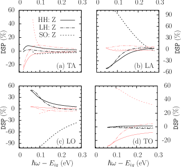
We now turn to resolving the spin injection rates into contributions from different valence bands. The results are similar to the corresponding resolution of carrier injection rates. The HH band gives the largest contribution due to its large density of states, while the SO band gives the smallest. However, there are subtleties in the DSP of injected spins from each valence band. In Fig. 14 we give the valence band and phonon-resolved spectra of the DSP. While the band edge values of the DSP are consistent with results in Table 4, the spin polarization direction shows a complicated energy dependence based on whether or not the band edge DSP is zero. For processes with nonzero band edge values, the DSP decrease from the nonzero values. For processes with zero band edge values, the DSP increase to a maximum value, and then decrease. Some of these DSP change sign with increasing photon energy.
VI.2.2 Spin injection at high temperature
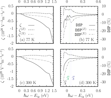
In Fig. 15 we plot the spectra of spin injection rates at 77 K and 300 K. In contrast to the carrier injection rates, which increase considerably from 77 K to 300 K, both the total spin injection rates and the rates in each valley change little from 77 K [Fig. 15 (a)] to 300 K [Fig. 15 (c)]. In order to show clearly the spin injection at the injection edge, the DSP are plotted in (b) and (d) respectively. the phonon absorption process becomes increasingly important as the temperature rises, and is shown by the left shifts of the onset of DSP to , which is determined by the TO/LO phonon absorption processes. In addition, the peak appearing at and 4 K in Fig. 12 (b) becomes fairly obscure at high temperature. These results can be better understood from the phonon-resolved DSP spectra at 300 K, given in Fig. 16.
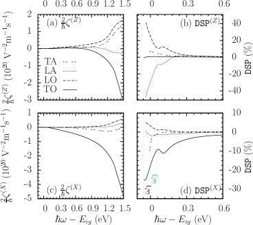
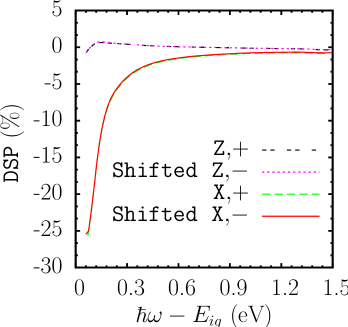
For the spin injection rates in the valley, shown in Fig. 16 (a), the contribution from each phonon branch is still of the same order of magnitude, but the TO phonon-assisted process dominates the injection at high photon energy. For the spin injection rates in the valley, shown in Fig. 16 (c), the contribution from the TO phonon branch dominates for all photon energies. However, the DSP, plotted in Figs. 16 (b) and (d), show finer structure in the low photon energy region than the DSP at 4 K. The fine structure is induced by the combined effect of the phonon emission and phonon absorption processes, which take effect at 300 K with considerable equilibrium phonon numbers for all phonon branches. According to the simplified Eq. (11), the injection rates for phonon absorption/emission processes differ from the JDOS, , at low photon energy. Therefore, spectra of DSP for these two processes have similar lineshapes, except for a phonon energy shift left or right. This conclusion is confirmed by our numerical results, shown in Fig. 17. Here the DSP from TO phonon absorption and emission processes are plotted for spins in both and valleys at 300 K, and all the absorption curves are right shifted by . The overlap is obvious. Based on these results, we return to Fig. 16.
We consider the DSP from the TO phonon-assisted process in the valley, shown as solid curve in Fig. 16 (d), is taken as an example. The spectrum in is induced by the phonon absorption processes, and decreases with increasing photon energy. When the photon energy is higher than , the TO phonon emission process comes into play. However, the spin injection rate for phonon emission is approximately proportional to , while that for phonon absorption is proportional to ; thus the former gives much larger injection rates than the latter. This results in a peak in the total DSP for the TO phonon-assisted process, at energies where phonon emission becomes important.
VI.2.3 Temperature dependence of spin injection

Fig. 18 shows the temperature dependence of the DSP at the different photon energies . For photon energy , all DSPs are temperature-independent: The TO phonon absorption process is the only process at this photon energy, and the injection rates of carriers and spins are approximately proportional to ; the two rates therefore scale the same with temperature, leading to a temperature-independent DSP. We check the temperature dependence of the DSP for all phonon branches at photon energy eV in Fig. 19. All these DSP are independent of temperature. This conclusion is valid for all photon energies considered to this point in this paper. However, the total DSP, shown in Figs. 18 (b), (c), and (d), are temperature dependent. At the indicated photon energies, more than one phonon branch makes a contribution. The injection rates for different phonon branches have different temperature dependences due to the different phonon energies. The ratio between the total injection rates of carriers and spins, i.e. the DSP, thus becomes temperature-dependent.

At high temperature, is approximately valid for all phonon branches, so the injection coefficients of and are approximately proportional to and give a constant DSP as saturation value. This is shown in Fig. 18.
VII conclusion
In conclusion, we have performed a full band structure calculation to investigate the indirect optical carrier and spin injection in bulk silicon. The injection spectra for carriers, spins, and DSP in each valley are studied in detail at different temperatures. The indirect gap injection is dominated by the transition from the HH band to the lowest conduction band due to the large JDOS. When incident light is propagating along one principal axis, the injection shows strong valley anisotropy. The injection rates induced by each phonon-assisted process increase with temperature. For carrier injection, we find that in the valley the TO phonon-assisted process dominates up to 300 K; in the valley, it only dominates at low temperature, while the injection rates induced by the TA phonon-assisted process increases to a comparable value at 300 K. The higher the photon energy, the weaker the temperature dependence. For spin injection, we find that injected spins in the and valleys have opposite polarization directions. In the valley, the LO phonon-assisted process dominates around the band edge, while the TO phonon-assisted process dominates at high photon energy; in the valley, the TO phonon-assisted process dominates for all photon energies.
The calculated absorption coefficients are in good agreement with experiments at high photon energy. Experience from direct gap absorption might lead one to believe this would not hold, since first principle studies of direct optical absorption in Si and GaAsPhys.Rev.B_62_4927_2000_Rohlfing ; Rev.Mod.Phys._74_601_2002_Onida ; Phys.Rev.B_71_195209_2005_Leitsmann demonstrated that the electron-hole interaction plays an important role even for high photon energy. Full band structure calculations of indirect gap absorption, including electron-hole interaction, have yet to be done, and the effect of these interaction on the indirect absorption coefficient at high photon energies have yet to be established. In any event, since to first approximation the nearly spin-independent electron-hole interaction will modify spin and carrier injections in the same way, it is reasonable to expect that the DSP of injected electrons in exciton continuum states will be insensitive to this interaction, which we neglect. Future work to confirm this is clearly in order, but in the interim we feel our study constitutes a good first investigation.
The DSP spectra excibit a rich variety of behaviours. At 4 K, the maximum DSP is about for photon energy ; absorption at this temperature and energy is dominant by TA phonon emission process. With increasing temperature, the phonon absorption processes become important, and the DSP for this photon energy decreases quickly. At 300 K, the maximum DSP appears at the photon energy as a value , which only comes from the TO phonon absorption assisted process, and is temperature-independent. The DSP in the valley can reach a maximum value at 4 K and at 300 K; both are larger than the total value and the value in the valley. Compared to bulk silicon, it should therefore be more efficient to inject spin in a confined silicon structure, where conduction band valleys are splitted.
Acknowledgements.
This work was supported by Natural Sciences and Engineering Research Council of Canada. J.L.C acknowledges support from China Postdoctoral Science Foundation. J.R. acknowledges support from FQRNT. J.F. acknowledges support from DFG SPP1285.Appendix A Modified Tetrahedron Summation
Both Eq. (6) and the JDOS in Eq. (12) are of the following form
| (27) | |||||
Here the integration spaces and are the irreducible BZ wedges, which are confined by the , , , , and points of a fcc Brillouin zone. Our numerical scheme is based on the improved LATM Phys.Rev.B_49_16223_1994_Blochl ; Phys.Rev.B_76_205113_2007_Nastos . We divide () into () small tetrahedra as () with vertices (). By a simple transformation, Eq. (27) becomes
with
and
| (29) |
In obtaining the equations above, we approximate the phonon energy to be a fixed value between the two small tetrahedra and . Now the Eqs. (LABEL:eq:app2) and (29) have the same shape, so we only discuss Eq. (29) in the following. Though the tetrahedron method can be applied to Eq. (29) directly, we avoid doing this because the transition matrix elements are obtained within the scheme of the EPM, which are very time-consuming in calculation for each pair. However, the direct tetrahedron method needs more points for convergence than is computationally feasible. Instead, since the dependence of the transition matrix elements on and is weak, we linearly interpolate in tetrahedron as
with being the position of four vertices of this tetrahedron, and being the linear interpolation function related to the vertex. Then Eq. (29) becomes
| (30) |
In the same way, we get for Eq. (LABEL:eq:app2). Then we find
and
| (31) | |||||
with
| (32) |
In the above equations, we replace by .
In indirect absorption, the excited holes are located around the top of the valence band, while the electrons are around the band edge of the conduction band. So we use a different division for and . With the division points and , we use the Delaunay triangulation method from the CGAL packagecgal to set up the tetrahedra. In these tetrahedra, the weights and can be calculated. However, the integration includes a function, which is a fast-varying function in space, and the present tetrahedron is too rough to obtain the weights with required precision. We refine this tetrahedron into smaller ones.
In our calculation, the division depends on the band structure. For conduction bands and the heavy hole band, or are generated with their distance not larger than , while for light hole and spin split-off bands, the distances become and , respectively. For the heavy hole grid, the accurate weights can be obtained by refining each tetrahedron as smaller ones (each edge is refined into 8 parts).
The convergence of the results is examined for the injection from heavy hole band to conduction band by changing the division points distance to . The difference between the injection rates from these two divisions is less than 5%.
References
- (1) F. Meier and B. Zakharchenya, Optical Orientation (North-Holland, Amsterdam, 1984).
- (2) I. Žutić, J. Fabian, and S. Das Sarma, Rev. Mod. Phys. 76, 323 (2004).
- (3) J. Fabian, A. M.-Abiague, C. Ertler, P. Stano, and I. Žutić, Acta Phys. Slovaca 57, 565 (2007).
- (4) M. W. Wu, J. H. Jiang, and M. Q. Weng, Phys. Rep. 493, 61 (2010).
- (5) G. G. Macfarlane, T. P. McLean, J. E. Quarrington, and V. Roberts, Phys. Rev. 111, 1245 (1958).
- (6) M. A. Green and M. J. Keevers, Prog. Photovolt: Res. Appl. 3, 189 (1995).
- (7) T. Suemoto, K. Tanaka, A. Nakajima, and T. Itakura, Phys. Rev. Lett. 70, 3659 (1993).
- (8) V. Y. Mendeleyev, S. N. Skovorodko, E. N. Lubnin, and V. M. Prosvirikov, Appl. Phys. Lett. 93, 131916 (2008).
- (9) M. Saritaş and H. D. McKell, J. Appl. Phys. 61, 4923 (1987).
- (10) H. A. Weakliem and D. Redfield, J. Appl. Phys. 50, 1491 (1979).
- (11) R. J. Elliott, Phys. Rev. 108, 1384 (1957).
- (12) B. Y. Lao, J. D. Dow, and F. C. Weinstein, Phys. Rev. B 4, 4424 (1971).
- (13) B. Y. Lao, J. D. Dow, and F. C. Weinstein, Phys. Rev. Lett. 26, 499 (1971).
- (14) V. D. Kulakovskiǐ, G. E. Pikus, and V. B. Timofeev, Sov. Phys. Usp. 24, 815 (1981).
- (15) R. L. Hartman, Phys. Rev. 127, 765 (1962).
- (16) D. Dunn, Phys. Rev. 166, 822 (1968).
- (17) W. S. Chow, Phys. Rev. 185, 1056 (1969).
- (18) W. S. Chow, Phys. Rev. 185, 1062 (1969).
- (19) O. J. Glembocki and F. H. Pollak, Phys. Rev. Lett. 48, 413 (1982).
- (20) S. Bednarek and U. Rössler, Phys. Rev. Lett. 48, 1296 (1982).
- (21) M.-F. Li, Z.-Q. Gu, and J.-Q. Wang, Phys. Rev. B 42, 5714 (1990).
- (22) O. J. Glembocki and F. H. Pollak, Phys. Rev. B 25, 1193 (1982).
- (23) M. Klenner, C. Falter, and W. Ludwig, Annalen der Physik 504, 24 (1992).
- (24) F. Nastos, J. Rioux, M. Strimas-Mackey, B. S. Mendoza, and J. E. Sipe, Phys. Rev. B 76, 205113 (2007).
- (25) G. Lampel, Phys. Rev. Lett. 20, 491 (1968).
- (26) G. Lampel, Proc. 9th Int. Conf. Phys. Semicond. 2, 1139 (1968).
- (27) A. S. Verhulst, Ph.D. thesis, Stanford University, 2004.
- (28) P. Li and H. Dery, Phys. Rev. Lett. 105, 037204 (2010).
- (29) J. R. Chelikowsky and M. L. Cohen, Phys. Rev. B 10, 5095 (1974).
- (30) J. R. Chelikowsky and M. L. Cohen, Phys. Rev. B 14, 556 (1976).
- (31) G. Weisz, Phys. Rev. 149, 504 (1966).
- (32) W. Weber, Phys. Rev. B 15, 4789 (1977).
- (33) J. Rioux and J. E. Sipe, Phys. Rev. B 81, 155215 (2010).
- (34) J. L. Cheng, M. W. Wu, and J. Fabian, Phys. Rev. Lett. 104, 016601 (2010).
- (35) P. E. Blöchl, O. Jepsen, and O. K. Andersen, Phys. Rev. B 49, 16223 (1994).
- (36) P. Y. Yu and M. Cardona, Fundamentals of Semiconductors: Physics and Materials Properties (Springer Berlin Heidelberg, New York, 2005).
- (37) P. Lautenschlager, P. B. Allen, and M. Cardona, Phys. Rev. B 31, 2163 (1985).
- (38) G. D. Mahan, J. Appl. Phys. 51, 2634 (1980).
- (39) W. Bludau, A. Onton, and W. Heinke, J. Appl. Phys. 45, 1846 (1974).
- (40) V. Alex, S. Finkbeiner, and J. Weber, J. Appl. Phys. 79, 6943 (1996).
- (41) M. M. Rieger and P. Vogl, Phys. Rev. B 48, 14276 (1993).
- (42) S. M. Sze, Physics of Semiconductor Devices (John Wiley and Sons, N. Y., 1981).
- (43) M. Rohlfing and S. G. Louie, Phys. Rev. B 62, 4927 (2000).
- (44) G. Onida, L. Reining, and A. Rubio, Rev. Mod. Phys. 74, 601 (2002).
- (45) R. Leitsmann, W. G. Schmidt, P. H. Hahn, and F. Bechstedt, Phys. Rev. B 71, 195209 (2005).
- (46) Cgal, Computational Geometry Algorithms Library, http://www.cgal.org.