Ultrafast Linear Kinetic Inductive Photoresponse of YBa2Cu3O7-δ Meander-Line Structures by Photoimpedance Measurements
Abstract
We report the experimental demonstration of the linear kinetic-inductive photoresponse of thin-film YBa2Cu3O7-δ (YBCO) meander-line structures, where the photoresponse amplitude, full-width-half-maximum (FWHM), and rise-time are bilinear in the incident optical power and bias current. This bilinear behavior reveals a trade-off between obtaining high responsivity and high speed photodetection. We also report a rise-time as short as 29ps in our photoimpedance measurements.
The interaction of light with superconducting samples is long known to perturb superconductivity Owen and Scalapino (1972); Sai-Halasz et al. (1974); Perrin and Vanneste (1983); Frenkel (1993), which can be used as a probing mechanism for optoelectronic applicationsTestardi (1971); Bluzer (1991); Adam et al. (1999); Enomoto and Murakami (1986); Kwok, Zheng, and Ying (1989); Leung et al. (1987); Brocklesby et al. (1989); Forrester et al. (1989); Hegmann and Preston (1993). In general, photons of energy greater than the Cooper pair binding energy () can initiate a chain of pair-breaking events resulting in a deviation of the quasiparticle and pair densities from their equilibrium values. Typically, these distributions depend on temperature, optical power and wavelength, thermal boundary conditions, and material properties such as electron-electron and electron-phonon interactions times, electron density, coherence length, penetration depth, and geometryBluzer (1991); Pals et al. (1982). While determining the spatial and temporal distribution of quasiparticles and pairs under a time-varying optical illumination is a profound problem in non-equilibrium superconductivity, many of the important concepts of such an interaction for device applications can be captured by means of a much simpler and more phenomenological approach, namely the kinetic inductance model Hegmann and Preston (1993). Within the kinetic inductance model the presence of the superconductive condensate, at a macroscopic level, can be adequately modeled by an additional inductive channel for charge transport. The optically initiated pair breaking mechanism, within this framework, should be interpreted as the spatial and temporal variations of the kinetic inductance and the normal resistance of the superconducting specimen.
Many researchers have experimentally studied the kinetic inductive photoresponse of superconducting thin films through photoimpedance measurements Bluzer (1991); Johnson (1991). In photoimpedance measurements, light induced changes in the microwave impedance of the superconducting structure are measured by an external high-frequency circuit. In its simplest form, the specimen is externally biased with a dc current and connected to a fast oscilloscope in series with a high bandwidth amplifier; absorption of optical photons then changes the impedance of the sample and produces a transient voltage response. A number of previous works have reported photoimpedance measurements on different superconductors mainly concluding that: 1) the resistive photoresponse dominates at temperatures well below the critical temperature (Tc), whereas the kinetic inductive response becomes the main mechanism of photoresponse close to Tc; 2) In the kinetic inductive regime the photoresponse could be very fast, with a rise time as low as 50ps, and is mainly limited by the time constants of the peripheral measuring apparatus; 3) the dependence of the photoresponse amplitude varies nonlinearly with the incident optical power.
The nonlinearity of the kinetic inductive photoresponse intrinsically arises from the nonlinear dependence of the kinetic inductance of a superconducting sample on the Cooper pair density. Therefore, even though changes in the Cooper pair density, under certain conditions, may vary linearly with the incident optical power, the resultant variation of the kinetic inductance is generally nonlinear. This point can be readily observed for a thin-film sampleOrlando and Delin (1991):
| (1) |
where is the kinetic inductance, and are the length and the cross section area of the sample, and respectively are the mass and charge of a Cooper pair, and is the density of Cooper pairs. Accordingly, the kinetic inductive photoresponse approximately readsAdam et al. (1999)
| (2) |
where is the bias current. Nevertheless, we have theoretically shown elsewhereGhamsari and Majedi (2008); Ghamsari (2010) that if the optical power and the bias current are far from their critical values, and the temperature is not too close to Tc the kinetic inductive response can be linearized giving a frequency-dependent voltage responsivity
| (3) |
where and are the incident optical power and modulation frequency, is the pair breaking efficiency, is the Cooper pairs recombination life time, and and are the equilibrium normal resistance and kinetic inductance of the sample in the absence of illumination. This regime of operation is particularly useful for optoelectronic device applications such as photodetectors and optically tunable microwave-photonic devices such as delay lines, resonators, and filters where linear tunability is highly desirable Atikian, Ghamsari, and Majedi (2010).
To serve as a detecting element, we have used a 100nm-thick YBCO thin film (THEVA, Ismaning, Germany) meander line structure with 5-m line widths and slots, covering an area of 176m200m. The meander line structure is placed at the midpoint of the center strip of a 50GHz-bandwidth 50 superconducting coplanar waveguide (CPW) transmission line. Figure 1 shows the image of the meander line and the current-voltage characteristics at 77K. The critical current is found to be 13mA, and the bias current is selected to be below this value. The meander line is externally dc biased through high bandwidth bias-tees. One end of the CPW is terminated with a 50 load to suppress any reflected signals. The other end is connected to a high-bandwidth microwave amplifier with a gain of 28dB, followed by a fast oscilloscope where the response to a train of 1550nm wavelength, 45ps-wide Gaussian optical pulses is measured. A block diagram of the measurement setup is shown in Figure 2. More details in regards to the photoimpedance experimental setup can be found in Atikian (2009).
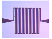
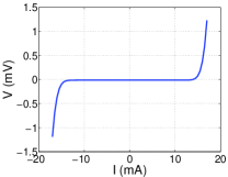
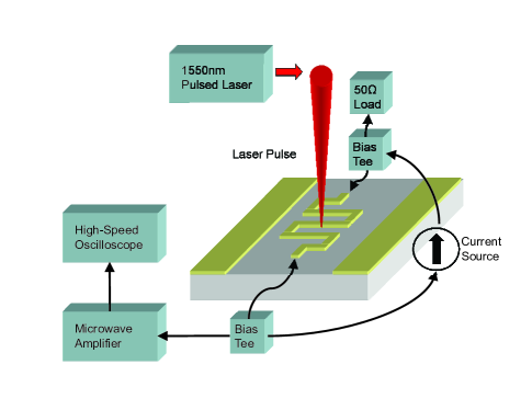
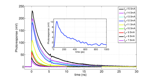
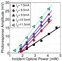
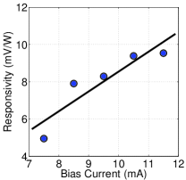
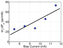
Figure 3 illustrates typical photoresponse waveforms for different bias currents at an incident optical power of 1.6mW. The inset of Figure 3 illustrates an operating point where we have measured rise times as short as 29ps. Figure 4a shows that the photoresponse amplitudes of the detector, for fixed bias currents, varies linearly with the incident optical power. Moreover, Figure 4b demonstrates that the responsivity of the device has a linear dependence on the bias current. These two observations confirm our previous theoretical prediction of the linear kinetic inductive response represented by equation (3). This linear response sustains as long as the perturbation in both kinetic inductance and normal resistance is small. This also implies that the fractional change in both the Cooper pair density and quasiparticles is small. These values, in general, depend on temperature, bias current, and average incident optical power. The linear regime of operation for this device, at a given temperature, is clearly illustrated by the range of current and optical power values in Figure 4.
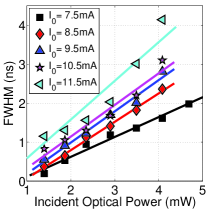
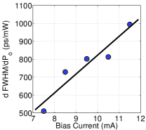
The FWHM of the photoresponse is a measure of the photoinduced disturbance in the detector, which according to (2) equals to . The perturbation in the kinetic inductance, , in the linear kinetic inductive regime, linearly varies with optical power and is independent of the bias currentGhamsari (2010). Thus, the product, and consequently the FWHM, should be bilinear in the optical power and bias current which is clearly shown by Figure 5. This point readily reveals the trade off between obtaining high responsivity and short photoresponse waveforms in linear kinetic inductive detectors, because the former requires a higher bias current whereas the latter demands a small bias current.
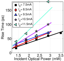
In addition to amplitude and FWHM, the rise time of the photoresponse waveform is also bilinear in optical power and bias current, as illustrated by Figure 6. In terms of an electrical circuit model, the detector acts like an RL circuit with time varying and , and a constant total current Ghamsari (2010). In this scenario, the rise time depends on the , which was shown to be bilinear in current and optical power. This point once again manifests itself as a trade-off between speed and responsivity in the linear regime. A set of similar results was obtained for a meander line with 3m line and slot widths, for which the same trends as the presented device was observed.
In conclusion, we have characterized the linear kinetic inductive photoresponse of thin-film YBCO meander line structures, where the photoresponse amplitude, FWHM, and rise time of the waveforms are bilinear in optical power and bias current. For a given operating point, we have been able to measure a short 29ps rise time in the linear kinetic inductive regime.
We acknowledge support from OCE (Ontario Center of Excellence), NSERC (Natural Sciences and Engineering Research Council of Canada), and the ONR/Maryland Applied Electromagnetics Center Task D10 (contract No. N000140911190).
References
- Owen and Scalapino (1972) C. S. Owen and D. J. Scalapino, Phys. Rev. Lett. 28, 1559–1561 (1972).
- Sai-Halasz et al. (1974) G. A. Sai-Halasz, C. C. Chi, A. Denenstein, and D. N. Langenberg, Phys. Rev. Lett. 33, 215–219 (1974).
- Perrin and Vanneste (1983) N. Perrin and C. Vanneste, Phys. Rev. B 28, 5150–5159 (1983).
- Frenkel (1993) A. Frenkel, Phys. Rev. B 48, 9717–9725 (1993).
- Testardi (1971) L. R. Testardi, Phys. Rev. B 4, 2189–2196 (1971).
- Bluzer (1991) N. Bluzer, Phys. Rev. B 44, 10222–10233 (1991).
- Adam et al. (1999) R. Adam, M. Currie, R. Sobolewski, O. Harnack, and M. Darula, IEEE Trans. Appl. Supercond. 9, 4091–4094 (1999).
- Enomoto and Murakami (1986) Y. Enomoto and T. Murakami, J. Appl. Phys. 59, 3807 3814 (1986).
- Kwok, Zheng, and Ying (1989) H. S. Kwok, J. P. Zheng, and Q. Y. Ying, Appl. Phys. Lett. 54, 2473–2475 (1989).
- Leung et al. (1987) M. Leung, P. R. Broussard, J. H. Claassen, M. Usofsky, S. A. Wolf, and U. Strum, Appl. Phys. Lett. 51, 2046–2049 (1987).
- Brocklesby et al. (1989) W. S. Brocklesby, D. Monroe, A. F. J. Levi, M. Hong, S. H. Liou, J. Kwo, C. E. Rice, P. M. Mankiewich, and R. E. Howard, Appl. Phys. Lett. 54, 1175 1177 (1989).
- Forrester et al. (1989) M. G. Forrester, M. Gottlieb, J. R. Gavaler, and A. I. Braginski, IEEE Trans. Magnet. 25, 1327–1330 (1989).
- Hegmann and Preston (1993) F. A. Hegmann and J. S. Preston, Phys. Rev. B 48, 16023–16039 (1993).
- Pals et al. (1982) J. A. Pals, K. Weiss, P. M. T. M. van Atfekum, R. E. Horstman, and J. Wolter, Phys. Rep. 89, 323–390 (1982).
- Johnson (1991) M. Johnson, Appl. Phys. Lett. 59, 1371–1373 (1991).
- Orlando and Delin (1991) T. P. Orlando and K. A. Delin, (Addison-Wesley, Massachusetts, 1991).
- Ghamsari and Majedi (2008) B. G. Ghamsari and A. H. Majedi, Trans. Appl. Supercond. 18, 1761–1768 (2008).
- Ghamsari (2010) B. G. Ghamsari, Ph.D. thesis, University of Waterloo (2010).
- Atikian, Ghamsari, and Majedi (2010) H. A. Atikian, B. G. Ghamsari, and A. H. Majedi, IEEE Trans. Microwave Theory Tech. 58, 3320–3326 (2010).
- Atikian (2009) H. A. Atikian, Master’s thesis, University of Waterloo (2009).