Intrinsic electron-glassiness in strongly-localized Be films
Abstract
We present results of out–of-equilibrium transport measurements made on strongly-localized Beryllium films and demonstrate that these films exhibit all the earmarks of intrinsic electron-glasses. These include slow (logarithmic) relaxation, memory effects, and more importantly, the observation of a memory dip that has a characteristic width compatible with the carrier-concentration of beryllium. The latter is an empirical signature of the electron-glass. Comparing various non-equilibrium attributes of the beryllium films with other systems that exhibit intrinsic electron-glasses behavior reveals that high carrier-concentration is their only common feature rather than the specifics of the disorder that rendered them insulating. It is suggested that this should be taken as an important hint for any theory that attempts to account for the surprisingly slow relaxation times observed in these systems.
pacs:
72.20.Ee 72.20.Ht 72.70.+m
I Introduction
The interplay between static disorder and Coulomb interactions may precipitate a glassy state in an Anderson insulator. This ‘electron-glass’ scenario was discussed in several papers 1 ; 2 ; 3 ; 4 . In theory, this property is generic to all degenerate Fermi systems with localized states interacting via a Coulomb potential. Experimental evidence for these glassy effects, however, has been somewhat scarce, presumably due to specific material requirements. It turns out that only systems with relatively high carrier-concentration exhibit relaxation times that can be conveniently monitored by transport measurements. Conductance relaxations that persist for many seconds, and memory effects characteristic of intrinsic 5 electron-glass, seem to be peculiar to systems with cm-3 5 . A prominent group of materials that exhibit electron-glass behavior with long relaxation times are granular metals; Al 6 , Bi 7 , Pb 7 , Ni 8 , and Au 9 , all having high carrier-concentration cm
Hitherto, the only non-granular systems that exhibited intrinsic electron-glass behavior were crystalline and amorphous indium-oxide films (In2O3-x and InxO respectively) 5 , which are ionic compounds.
In this work we report on the low temperature transport properties of strongly-localized Be films, and demonstrate that they exhibit intrinsic glassy effects. This is the first non-granular mono-atomic system to show these effects. These include logarithmic relaxation of the out-of-equilibrium conductance and, more importantly, a memory-dip that has all the earmarks of intrinsic electron-glass. Although beryllium, like a typical metal, has a Fermi energy EF of few electron-volts, it has an unusually low density of states at EF 10 . A signature of the Be peculiar density of states, namely, at the Fermi energy, the density-of-states decreases with energy, is actually observed in our field effect measurements as will be demonstrated below. The low density of states of beryllium is presumably the main reason why strong localization is achievable in this material just by making the sample thin enough (yet still physically continuous).
II Experimental
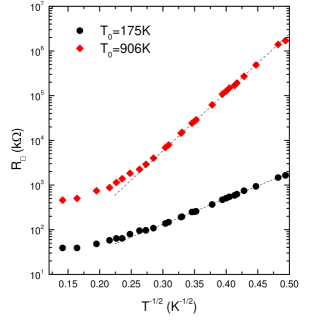
Samples used in the experiments reported here were 185Å films deposited as described elsewhere 11 on 140m glass slides. These were silver-painted on their backside so as to form a gate for the field effect measurements. The samples were typically 400m wide and 600m long strips and had sheet resistance R□ in the range 23k to 120k at 295K and 100k-160M at 4K. The strongly-localized nature of the films at this temperature range was tested by measuring their conductance versus temperature dependence G(T) in the range 4-50K. Below10K, this dependence is consistent with G(T)[-()1/2] with T0 in the range 100-900K. Figure 1 illustrates this behavior for two of the samples that were used in this study.
The different values of R□ in the studied series of samples were obtained by a judicious oxidation of the Be films in an oxygen-enriched chamber. The change of the samples resistance was constantly monitored during the oxidation process. At the range of sample thickness d 18 Å, the room-temperature sheet-resistance of the samples is 20k. Such samples are usually deep into the hopping regime at liquid helium temperatures, and a small change in their thickness d translates into a large change of R□ at 4K. The sheet-resistance of samples much thicker than 18 Å may not reach the quantum resistance at 4K (recall that R□/e2 is a pre-requisite for electron-glass behavior 5 ). For example, in a previous study 12 a beryllium film with a nominal thickness d of 20 Å, only slightly thicker than the films studied here, exhibited G(T)[-()1/2] with T0=1.6K. This should be compared with T100K in the samples used in this work. The much smaller value for T0, and the associated larger localization length in this case means that strongly-localized behavior is attained only at temperatures that are well below the range covered here. Such samples are not included in our present study where one of our goals is to compare the results with previously studied electron-glasses, which were measured at or near 4K.
The conductivity of the samples was measured using a two-terminal ac technique employing a 1211-ITHACO current pre-amplifier and a PAR-124A lock-in amplifier. Measurements reported below were performed with the samples immersed in liquid helium at T=4.1K maintained by a 100 liters storage-dewar, which allowed long term measurements of samples as well as a convenient way to maintain a stable temperature bath. Unless otherwise indicated, the ac voltage bias was small enough to ensure linear response conditions (judged by Ohm’s law being obeyed within the experimental error). Fuller details of measurements techniques are given elsewhere 13 .
A variety of techniques were employed to characterize the films microstructure. Fig.2 shows a Transmission Electron Microscope (TEM) micrograph of a Be film prepared in the same way and with similar thickness as the samples used for the transport studies.
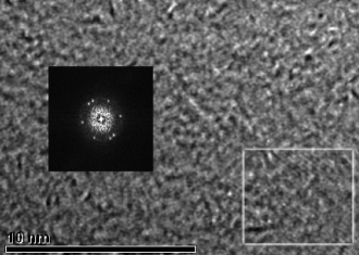
The physical continuity of the film is evident in the figure. On careful examination, the micrograph shows occasional fringes that indicate the presence of small crystals. These were identified as BeO by direct imaging and further, by their diffraction pattern (interestingly, the diffraction pattern of Be, being light on electrons, was presumably too weak to register a clear pattern over the background set by the amorphous carbon support-film). The BeO crystals were clearly observable in TEM dark-field imaging off their 100 diffraction line. This enabled an estimate of their crystallographic size and partial volume in the samples. Randomly distributed BeO crystallites of sizes up to 50-70Å were observed in these dark-field images. We estimate that less than 10% of the film area is occupied by fully oxidized Be crystallites, and therefore transport presumably occur through non-oxidized Be phase. Yet, the insulating BeO crystallites, somewhat restrict the volume available for conductivity (much like punching holes in the film would). A result of this geometrically-constrained structure is that the transport properties of the films show some mesoscopic effects that one usually encounters in smaller systems measured at similar temperatures and comparable degree of disorder 14 ; 19 .
The physical continuity of the Be phase in the film was ascertained by performing local electron-energy-loss-spectroscopy (EELS) on the parts of the film that were not occupied by BeO crystals. The EELS spectra taken from theses areas was consistent with that of metallic Be. A slight shift of energy, +3% of the peaks position in the spectra was detected, possibly due to strain. The presence of free Be in the samples was also confirmed by X-ray Photoemission Spectroscopy, which was carried out on the actual samples that were used for the transport measurements.
III Results and discussion
We turn now to the non-equilibrium transport properties of the films. The first signature of glassy behavior in these films is encountered upon quench-cooling the sample to 4K; after an initial fast drop (reflecting the change in temperature), the conductance G keeps on decreasing slowly (logarithmically) long after the sample has reached the bath temperature. A typical quench-cooling protocol is shown in Fig.3a.
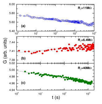
The figure also illustrates the slow conductance excitation process upon ‘stressing’ 15 the film with a non-Ohmic source-drain voltage Fig.3b. The ensuing relaxation of G after the source-drain voltage was set back to its Ohmic value is shown in Fig.3c. These excitation-relaxation curves are clearly similar to those previously observed in glassy In2O3-x samples 15
A controlled way to take the system out of equilibrium is a change of the potential difference between the sample and a near-by gate. This technique has been widely used in the study of several electron-glasses 5 ; 6 ; 7 ; 13 . Among other things, it may be used to estimate a typical relaxation time under a given set of conditions 16 . An example of such protocol is illustrated in Fig.4.
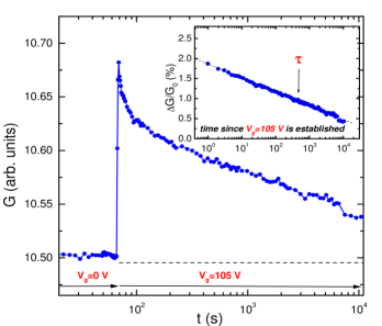
In this protocol, one uses the conductance relaxation law G(t/t0)G(t/t0) where t0 is the experimental resolution time, and the equilibrium value of G at Vg=105V to extract the value of defined by GG
A characteristic feature that is believed to be common to all intrinsic electron-glasses is a memory-dip; this is a cusp-like minimum in G(Vg) centered at the gate voltage Vg where the system was allowed to equilibrate 5 ; 6 ; 7 ; 17 . A conspicuous memory-dip was consistently observed in all our Be films. Fig.5 shows this feature for two Be samples in the studied series. For both samples, G(Vg) scans were taken after a 24 hour equilibration under Vg=0 volt. Note first that the memory-dips have the same shape and width independent of R□ and independent of wether the G(Vg) scans were taken by sweeping Vg through the equilibrium-Vg or symmetrically around it 13 (c.f., the lower graph of Fig.5).
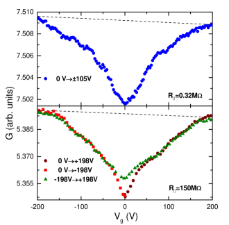
In previously studied electron-glasses the width of the memory-dip was found to systematically depend on the carrier-concentration of the system 17 . On the basis of the G(Vg) data, we have estimated the typical width in our Be films in the same manner as was done in 17 . This involves several stages; First the change of charge Q associated with the cusp-width is estimated from Vg by taking heed of the sample-gate capacitance. The relevant energy is then calculated using the beryllium (n/) and the screening length. This procedure gave the energy-width (as defined in 17 ) as 8meV. Using the empirical relation between the width and (Fig.4 of 17 ) such corresponds to of order 1021-1022cm-3. This is consistent with our Hall effect measurements that gave 7-81021cm-3 as well as with the concentration predicted by band-structure calculations ( = 0.016 state/atom 18 tantamount to cm-3). This correlation between the width of the memory-dip and the carrier concentration of the material is an important empirical test for the intrinsic nature of the electron-glass 5 .
The G(Vg) traces (Fig.5) reveal some mesoscopic fluctuations (reproducible with Vg scans) superimposed on the memory-dip (note e.g., the modulation of G(Vg) around V120V, and +90 for the 0.32M and the 150M samples respectively). As alluded to above, these presumably result from the small effective volume for conductance due to the presence of the insulating BeO regions.
The relative magnitude of the memory-dip G/G grows monotonously with R□. Interestingly, G/G(R□) for Be is almost identical to that measured under the same conditions in other electron-glasses. In Fig.6 we compare the results of the current study with some old data 19 taken on In2O3-x films exhibiting quite similar behavior.
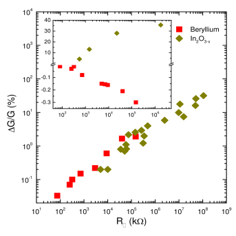
A similar agreement is observed between that data of Fig.6 and the results obtained on granular aluminum films (c.f., Fig.17 of 20 ).
On the other hand, the anti-symmetric part (c.f., Fig.6) of the G(Vg) for the beryllium samples has the opposite slope to that observed in In2O3-x and InxO 5 ; 13 . The sign of this slope is controlled by the energy derivative of the thermodynamic density of states n/ at the Fermi level; G(Vg)/V(n/). The anti-symmetric part of G(Vg)/Vg we observe in all our Be films (represented by the dashed curves in Fig.5) is consistent with the negative slope of n/ found in theoretical calculations for the Be band-structure 21 . These calculations assumed an ideal Be crystal which might not be relevant for the disordered structure. It is not uncommon however that band-structure features calculated for the perfect crystal persist in the disordered material (as actually observed for some optical properties of Be 22 ). The magnitude of the slope depends also on the film resistance as is shown for both In2O3-x and Be in the insert to Fig.6. Being a low density system, (n/) in In2O3-x is much larger than in metals, which in turn makes G(Vg)/Vg larger.
It is interesting to note that the currently known electronic systems that exhibit intrinsic glassiness (with associated long relaxation times) are quite diverse in most other aspects. For example, in terms of microstructure, there are in this group representatives of all types of disordered structures; poly-crystalline (In2O3-x, and Be), granular or discontinuous (Al, Pb, Au, Ni), and amorphous (InxO, Bi). Most of these systems contain oxide, whether as an intrinsic part of the material (In2OInxO), or to stabilize a granular structure (e.g., Al). However, the discontinuous Ni films, being prepared and measured under high-vacuum conditions 8 , is oxygen-free and show the same effects as the other intrinsic electron-glasses 8 . In some of these systems there may be local order due to superconductivity (Pb, Bi, the high n version of InxO, Be, Al) or magnetism (Ni) at the temperatures of the experiments but not in others. Finally, all these systems obey some form of activated conductivity, G(T)[-()α] with 0.31, however, no single value of is singled out in the group. In other words, the conductivity versus temperature law G(T) exhibited by these systems is not due to a specific hopping mechanism. It does not set this group apart from other hopping systems that do not exhibit long relaxation times. Indeed, a G(T) law that resembles is observed in many disordered semiconductors while their relaxation times are very short 23 (presumably due to their low 5 ).
In fact, the only common feature of the materials that show long relaxation times appears to be their relatively high carrier-concentration (in addition of course to being strongly-localized thus exhibiting hopping conductivity). The common, out-of-equilibrium features that all these electron-glasses exhibit are suggestive of a generic mechanism. The current work supports the conjecture that sluggish relaxation and the associated memory effects of the electron-glass is intimately connected with high carrier-concentration 5 . This should be the pivotal point of any theoretical model that purports to account for these phenomena.
ZO and PWA gratefully acknowledge discussions with the participants of the Electron-Glass program (organized by the Kavli Institute of Theoretical Physics) during which this manuscript was prepared. This research was supported by a grant administered by the US Israel Binational Science Foundation and by the Israeli Foundation for Sciences and Humanities. PWA acknowledges the support of the US Department of Energy under Grant No. DE-FG02-07ER46420.
References
- (1) J. H. Davies, P. A. Lee, and T. M. Rice, Phys. Rev. Lett., 49, 758 (1982).
- (2) M. Grünewald, B. Pohlman, L. Schweitzer, and D. Würtz, J. Phys. C, 15, L1153 (1982).
- (3) M. Pollak and M. Ortuño, Sol. Energy Mater., 8, 81 (1982); M. Pollak, Phil. Mag. B 50, 265 (1984).
- (4) Ariel Amir, Yuval Oreg, and Yoseph Imry, Phys. Rev. B 77, 165207 (2008).; Phys. Rev. Lett. 103, 126403 (2009).
- (5) Z. Ovadyahu, Phys. Rev. B 78, 195120 (2008).
- (6) T. Grenet, Eur. Phys. J, 32, 275 (2003); T. Grenet, J. Delahaye, M. Sabra, and F. Gay, Eur. Phys. J. B 56, 183 (2007).
- (7) G. Martinez-Arizala, D. E. Grupp, C. Christiansen, A. Mack, N. Markovic, Y. Seguchi, and A. M. Goldman, Phys. Rev. Lett., 78, 1130 (1997). G. Martinez-Arizala, C. Christiansen, D. E. Grupp, N. Markovic, A. Mack, and A. M. Goldman, Phys. Rev. B 57, R670 (1998).
- (8) A. Frydman (in private communication).
- (9) C. J. Adkins, J. D. Benjamin, J. M. D. Thomas, J W Gardner, and A. J. McGeown J. Phys. C: Solid State Phys. 17, 4633 (1984). Note however that no time dependence of the effects has been reported in this paper.
- (10) Guenter Ahlers, Phys. Rev. 145, 419 (1966).
- (11) P. W. Adams, P. Herron, and E. I. Meletis, Phys. Rev. B, 58, R2952 (1998).
- (12) V. Yu. Butko, J. F. DiTusa, and P. W. Adams, Phys. Rev. Lett., 84, 1543 (2000); V.Yu. Butko and P.W. Adams, Nature 409, 161 (2001).
- (13) A. Vaknin, Z. Ovadyahu, and M. Pollak, Phys. Rev. B 65, 134208 (2002).
- (14) V. Orlyanchik, and Z. Ovadyahu, Phys. Rev. B 75, 174205 (2007).
- (15) V. Orlyanchik, A Vaknin, and Z. Ovadyahu, Phys. Stat. Sol., B 230, 67 (2002); V. Orlyanchik, and Z. Ovadyahu, Phys. Rev. Lett., 92, 066801 (2004).
- (16) Z. Ovadyahu, Phys. Rev. B 73, 214208 (2006).
- (17) A. Vaknin, Z. Ovadyhau, and M. Pollak, Phys. Rev. Lett., 81, 669 (1998).
- (18) J. H. Tripp, P. M. Everett, W. L. Gordon, and R. W. Stark, Phys. Rev., 180, 669 (1969).
- (19) M. Pollak and Z. Ovadyahu, J. de Physique I France, 7, 1595 (1997).
- (20) J. Delahaye, T. Grenet and F. Gay, Eur. Phys. J. B 65, 5 (2008).
- (21) E. Wimmer, J. Phys. F: Met. Phys. 14, 681 (1984); G. Pari, Vijay Kumar, A. Mookerjee, and A. K. Bhattacharyya, J. Phys.: Condens. Matter 11, 4291 (1999); R. Boc̃a, P. Hajko, and L. Benko, Czechoslovak J. of Physics, 44, 897 (1994).
- (22) O. Hunderi and H. .P Myers, J. Phys. F: Metal Phys., 4, 1088 (1974).
- (23) Don Monroe A. C. Gossard, J. H. English, B. Golding, W. H. Haemmerle, and M. A. Kastner, Phys. Rev. Lett. 59, 1148 (1987); V.K. Thorsmølle, and N.P. Armitage, Phys. Rev. Lett. 105, 086601 (2010).