Absence of scaling in transport through two-dimensional nanoparticle arrays
Abstract
We analyze the transport in disordered two-dimensional nanoparticle arrays. We show that the commonly used scaling hypothesis to fit the I-V curves does not describe the electronic transport in these systems. On the contrary, close to the threshold voltage the current depends linearly on . This linear behavior is observed for at least five decades in . Fitting the I-V curves at larger voltages to a scaling power-law results in fitting parameters which depend on the range of voltages used and in wrong values for . Our results urge to change the picture of electronic transport in disordered nanoparticle arrays used in the last two decades.
Since the pioneering work of Middleton and Wingreenmiddletonwingreen93 (MW) in 1993 the transport in disordered nanoparticle arrays has been interpreted in terms of a threshold voltage , the minimum bias voltage necessary to allow the flow of current, and I-V curves with power-law behavior . For charge disordered arrays and short-range interactions MW predicted and for one (1D) and two dimensions (2D) respectively. This power law is supposed to hold above, but arbitrarily close to the threshold voltage.
In the last decade a wide variety of 2D arrays has been available and their transport properties studiedgrzelczak10 ; zabet08 . Experimental I-V characteristics have been systematically discussed in terms of these power-lawsrimberg95 ; black00 ; jaeger01 ; ancona01 ; ancona03 ; romerodrndic05 ; elteto1d05 ; blunt07 ; tan09 ; sachser09 . The exponent observed is, on the other hand, larger, than expected in most of the experiments and frequently sample-dependent. Deviations of the observed exponent from the predicted value have been often interpreted in terms of a dimensionality of the experimental set-up larger than two. But the scaling exponent found in quasi-one dimensional strips was . To claim scaling behavior at least two decades in the scaling parameter should be desirable. Experimentally the power laws have never been observed in such a large range of voltages but, they have been in most cases restricted to less than a decade, somewhere in the region .
Numerical confirmation of the 2D exponent has been also elusive. For short range interactions, MW found for . Later, Jha and Middletonjhamiddleton05 failed to define a proper power-law. Similarly, for long-range interactionskaplan03 . The discrepancy was attributed to finite-size effectsmiddletonwingreen93 ; jhamiddleton05 . Interestingly, Jha and Middletonjhamiddleton05 argued that the voltages at which the exponents are found correspond to a region outside the putative MW regime. In this paper we show that the reason for all these discrepancies is that the power-law scaling description of MW fails.
The prediction of MW is based on the assumption that close to threshold the current flows through independent channels, each of them driving a current linearly dependent on . The number of channels depends on the dimensionality. For 1D systems . On the basis of a mapping of the current flow to a model of interface growthKPZ , which neglects the role of the contact junctions in determining the current, they concluded that in 2D systems , which together with the linear current of a 1D channel gives .
Recently we confirmed that 1D arrays show a linear dependence close to thresholdnosotrosprb08 . This linearity lasts for at least five orders in magnitude, see Fig. 1, but it disappears at voltages much smaller than those at which both experiments and previous numerical calculations were performed . Linearity arises from the voltage dependence of the tunneling rate at the contact junction (between array and electrodes) which acts as a bottle-neck for the current. Having in mind the influence of the contact junctions in 1D arrays close to threshold, we expect that in 2D systems the current is carried by a single channel and linear I-V curves with slope determined by the resistance of the contact junctions and the failure of MW prediction. At the voltages at which new conduction channels open the linear dependence of the first channel has disappeared invalidating MW assumptions.
In order to test the validity of MW scaling argument we have carried systematic numerical simulations in 2D systems. We have found that, as in 1D, in charge disordered 2D arrays close to threshold the current is carried by a single channel, and depends linearly on voltage. This dependence lasts for several decades, but disappears at small voltages, not accessible experimentally. With increasing voltage the I-V curves show a crossover which in large arrays resemble a super-linear power-law. Previous claims of scaling and power-laws have been done in the range of voltages at which we observe this crossover. However, fitting the crossover to a power-law produces threshold voltages and exponents which depend on the range of voltages used in the fitting and fail to give the correct value of the threshold.
We consider an array of metallic islands in the classical Coulomb blockade regime, with the charging energy, the single particle level spacing, the temperature and the Boltzmann constant. Temperature is then taken equal to zero. The array is placed in between two electrodes at voltages . The islands are separated between themselves and from the contacts by tunnel junctions. Except otherwise indicated we assume all the junctions to have the same resistance. Electronic interactions are assumed to be finite only when the charges are in the same conductor, i.e. capacitive coupling between different conductors vanishes. The electronic charge is taken equal to unity. Transport is treated at the sequential tunneling level. To compute the current we use a Monte-Carlo simulation, described previouslynosotrosprb08 ; likharev89 . We have studied clean and disordered arrays with square and triangular lattices and three types of disorder: charge disorder, resistance disorder and structural disorder, i.e. voids in the lattice.
Before discussing two-dimensional systems we review the transport in 1D charge disordered -particle arrays nosotrosprb08 and show that while linearity lasts for several orders of magnitude, proper scaling in the MW sense is not present. As discussed above, the current is blocked up to a threshold voltage which depends on the disorder configuration. Below charges entering from the electrodes pile-up inside the array and create charge gradients which overcome the upward steps in the disorder potentialmiddletonwingreen93 . At a charge entering from the electrodes is able to flow through all the array. Above, but very close to the threshold the entrance of charges onto the array act as a bottle neck for the current. The current can be approximated by the tunneling rate at the contact junction which controls the entrance of charges to the arraynosotrosprb08 . This rate increases linearly with resulting in a current . Here is the resistance of the bottle neck junction. To understand this equation it is important to take into account the way in which the voltage (not to be confused with the total potential) drops through the array. For short-range interactions the voltage drops only at the contact junctions, between array and electrodesnosotrosprb08 .
The linearity close to threshold lasts for several orders of magnitudes, see Fig. 1(a). The slope is independent of the array size, while the threshold voltage, when averaged over disorder configurations is proportional to the number of particles middletonwingreen93 ; nosotrosprb08 . This means that proper scaling of the current in terms of does not occur, as observed in Fig. 1 (b). Disagreement with MW originates in the voltage drop through the array which they thought to be homogeneous. Deviations from linearity happen at small when the contact junction stops being the bottle-neck.
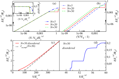
At high voltages () the current approaches with , and the sum of the tunnel resistances in series, see Fig. 1(c). In between these two linear regimes the current increases showing Coulomb staircase plateaux, see Fig. 1(d). Plateau-like behavior appears when the current is controlled by the tunneling through a junction which tunneling rate does not depend on the bias voltagenosotrosprb08 .
In 2D disordered arrays at voltages just above the threshold the current is carried by a single path. This is the path which requires the smallest pile-up of charges to overcome the disorder potential. Until a second path opens one might expect that the current looks like the one of a one-dimensional channel with slope controlled by the contact junction through which the charges enter. This is confirmed in Fig. 2. The linear behavior is observed in clean and disordered arrays with square or triangular lattice and in the presence of voids. It lasts for at least five orders in magnitude and disappears at values of similar to those found in 1D arrays, much smaller than those in experiments and previous numerical simulations. The derivative of the I-V curve in disordered arrays, equal in 1D and 2D, confirms that a single channel drives the current, see inset in Fig.2(a). In contrast, in clean arrays channels open at .
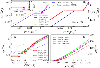
As in 1D, a linear dependence on does not mean scaling on . This is seen in Fig. 2 (a) where all the curves, corresponding to arrays with different , show the same current in the linear regime in units of . The whole lattice determines , but a single contact junction, controls the slope of the current close to threshold. To emphasize this, in Fig.2 (b) we plot the I-V of a disordered array with all the resistances equal and the I-V of the same array but with contact resistances between electrodes and array one thousand times smaller than those between the islands. In the array with small contact resistances the current is three orders of magnitude larger at low voltages. This confirms that the contact junctions, and not the lattice as usually assumed, control the current close to threshold. With increasing voltage it is the lattice who controls the current and the influence of the contact junction decreases.
The scaling behavior discussed by MW was partly based on how new channels open to current flow. Clearly, between the low voltage linear regime controlled by a single channel and the high voltage linear regime to which many channels contribute, there should be at least a crossover regime with channel opening. In Fig. 2 it is seen that in this crossover the I-V curves show clear steps with horizontal plateaux. Plateau-like features indicate that one or several inner junctions, with tunneling rates independent of bias voltage, act as bottle-neck for the current. Similar plateaux where observed in rimberg95 . Steps are associated to channel opening. The steps smooth with increasing array size as new channels open in smaller voltage intervals. On average, the current increases faster than linear and resembles a power-law in large arrays, see Fig. 2(d). As seen in Figs. 2(c) and 2(d), in the crossover range of voltages, the current of an disordered array does not scale with , nor . We note here that, as early discussed by Jha and Middletonjhamiddleton05 the range of voltages where the superlinear behavior is found is out of the close to threshold regime discussed by MW. In fact, this range is closer to the high-voltage regime, discussed below than to the close to threshold low voltage regime.
To make connection with experimental results we have checked the fitting parameters which are obtained when the I-V curves in this regime are fitted to a scaling power law of the kind proposed by MW, . In Fig. 3 (a) and (b) we perform fittings to the I-V curve of a charge disordered array, using this power-law expression, the value of , known theoretically, and the range of voltages plotted in each figure. The values of the exponents that we obtain are similar to the ones discussed in the literature. However, the fitting parameters, and in particular the scaling exponent, change considerably depending on how large it is the range of voltages used in the fitting, even if this range of voltages is quite small. This fact suggests that a power-law does not describe the current-voltage dependence.
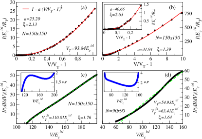
If such a power-law like were a good approximation to the current, plotting one could determine and . This method has been used experimentally to extract these parametersancona01 ; blunt07 ; ruffino07; sachser09 ; tan09 . In Fig. 3 (c) and (d) we show these functions for the array in (a) and (b) and for a array, with their corresponding fitting parameters. Notice that the obtained in the fitting does not equal the true one. One can go even further and derive these curves. Such a derivative should give a constant . As shown in the insets of Figs. 3 (c) and (d) these derivatives while giving are far from being constant. This fact confirms that the crossover is neither described by a power-law function and the failure of MW description in 2D arrays.
One might ask how important are finite-size effects and if the crossover region could extend to smaller voltages and converge to the predicted power-law in much larger systems. No features in our data suggests this to be the case. Within the range of sizes analyzed, with the number of particles varying between 400 and 29000, we have not found any systematic dependence of the voltage at which the superlinear crossover starts as a function of array size One could think that our lattices are still small. We now argue that this is not the case.
Let us consider an square lattice. For larger N, on average, the new channels could open for smaller values of as increasing the number of rows increases the possibilities to find a new path with a small threshold. On the other hand as the number of columns becomes larger the contact junction of the early open channels stops being the bottle-neck for smaller voltages and their linear current-voltage contribution is substituted by a plateau. Thus, it does not seem possible to satisfy the two assumptions of Middleton and Wingreen (channel opening and linear dependence) at the same time. But even if there were a way in which both assumptions were satisfied the linear behavior of each path would refer to its own path threshold voltage . is larger than the array , which is the voltage of the first path which opens. This means that this linearity would not scale with as assumed by MW implying that the derived equations would not be correct.
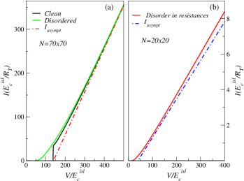
We end with a brief discussion of the large voltage regime. At high voltages, , and in the absence of voids, as in 1D the current is linear but extrapolate to zero at a finite offset voltage which keeps memory of the interaction effectsnosotrosprb08 ; kaplan03 . In the case of a square lattice, with no voids nor resistance disorder, the high-voltage regime can be approximated by with the sum of the junction resistances in row in series. This equation is valid for both clean and charge disordered systems, see Fig. 4 (a). On the other hand when the junction resistances are not all equal, the current cannot be approximated by this expression, see Fig. 4 (b). This originates in the meandering of charges to avoid large resistance junctions. A similar effect appears in lattices with voids.
In conclusion, we have shown that the scaling law of Middleton and Wingreenmiddletonwingreen93 and widely used since then, does not describe the I-V of 2D disordered arrays close to threshold. We find that close to threshold the current is controlled by the contact junctions which act as bottle-neck and not by the whole lattice as it was assumed in that work. Contrary to the prediction of a power-law with exponent , close to threshold the current depends linearly on . In the crossover region at larger voltages, our calculations agree with experimental results when trying to fit the I-V curves to a power-law scaling curve. However, such fitting results in meaningless fitting-parameters which depend on the range of voltage considered and in wrong values for . Our calculations urge to leave the scaling description for the transport in 2D systems, used during the last two decades.
Funding from Ministerio de Ciencia e Innovación through Grants No. FIS2008-00124, FPI fellowship and Ramón y Cajal contract, and from Consejería de Educación de la Comunidad Autónoma de Madrid and CSIC through Grants No. CCG07-CSIC/ESP-2323, CCG08-CSIC/ESP3518, PIE-200960I033 is acknowledged.
References
- (1) A.A. Middleton and N.S. Wingreen. Phys. Rev. Lett. 71, 3198 (1993).
- (2) M. Grzelczak et al, ACS Nano 4 3591, (2010).
- (3) A. Zabet-Khosousi and Al-A. Dhirani, Chem Rev. 108, 4072(2008).
- (4) A.J. Rimberg A.J., T.R. Ho and J. Clarke, Phys. Rev. Lett. 74, 4714 (1995). C.. Kurdak et al Phys. Rev. B 57, R6842 (1998).
- (5) C.T. Black et al Science, 290 1132 (2000).
- (6) R. Parthasarathy, X.M. Lin and H.M. Jaeger, Phys. Rev. Lett. 87, 186807 (2001).
- (7) M.G. Ancona et al, Phys. Rev. B 64, 033408 (2001).
- (8) M.G. Ancona et al, Nano Letters 3, 135 (2003).
- (9) H. E. Romero and M. Drndic, Phys. Rev. Lett. 95, 156801 (2005).
- (10) K. Elteto, X.M. Lin and H.M. Jaeger, Phys. Rev. B 71, 205412 (2005).
- (11) M. O. Blunt et al Nano Lett. 4, 855 (2007). F. Ruffino F. et al Journ. of Appl. Physics, 101, 024316 (2007).
- (12) R.P. Tan et al, Phys. Rev. B 79, 174428 (2009).
- (13) R. Sachser, F. Porrati and M. Huth. Phys. Rev. B, 80, 195416 (2009).
- (14) S. Jha and A.A. Middleton, cond-mat/0511094 (2005).
- (15) D.M. Kaplan, V.A. Sverdlov and K.K. Likharev, Phys. Rev. B, 68, 045321 (2003). C. Reichhardt and C.J. Olson Reichhardt, Phys. Rev. B 68, 165305 (2003).
- (16) M. Kardar, G. Parisi and Y-C. Zhang, Phys. Rev. Lett. 56, 889 (1986).
- (17) E. Bascones, V. Estévez, J.A. Trinidad, A.H. MacDonald, Phys. Rev. B, 77, 245422 (2008).
- (18) N.S. Bakhalov, G.S. Kazacha, K.K. Likharev, Sov. Phys. JetP,68, 581 (1989).