junction transition in InAs self-assembled quantum dot coupled with SQUID
Abstract
We report the transport measurements on the InAs self-assembled quantum dots (SAQDs) which have a unique structural zero-dimensionality, coupled to a superconducting quantum interference device (SQUID). Owing to the SQUID geometry, we directly observe a phase shift in the current phase relation and the negative supercurrent indicating junction behavior by not only tuning the energy level of SAQD by back-gate but also controlling the coupling between SAQD and electrodes by side-gate. Our results inspire new future quantum information devices which can link optical, spin, and superconducting state.
Recent advances in nanofabrication technology have made it possible to couple quantum dot (QD) with superconducting quantum interference device (SQUID), so that the combination of highly controllable electronic system and most sensitive detector for magnetic flux inspires new applications for future quantum information device. Up to date, the QD-SQUID has been studied by utilizing one-dimensional semiconductor nanostructures such as carbon nanotubesCleuziou:2006 and InAs nanowires Dam:2006 where the gate-controlled junction suggests that such configuration is very attractive for studying the spin states of an individual electron placed on the one of the two QD Josephson junctions in SQUID.
Besides one-dimensional nanostructure, it is noticeable for the recent researches of the self-assembled quantum dot (SAQD) as another type of QD. The SAQDs are grown by strain driven self-assembly onto a substrate, leading to spontaneous formation of small islands. Since it can be optically excited, controllably positioned, electronically coupled, and embedded into active devices, it is very attractive for the realization of optically programmable electron spin memory.Kroutvar:2004 Also note that the geometric structure can have better flexibility than one-dimensional nanostructure for complicated-circuit integration. Recently InAs SAQD has been coupled with superconductor via the nanogap method Jung:2005 and has been studied for the interplay between Kondo effect and superconductivity in SAQD.Buizert:2007 ; Deacon:2010 In spite of its versatility, it has not been yet reported for SAQD coupled to SQUID.
In this letter, we present the successful fabrication for the InAs SAQD coupled with SQUID by means of an electron beam (EB) lithography and an atomic force microscope (AFM) and the electrical transports involving gate-controlled junction transition of QD-SQUID.
In our experiment, the InAs SAQDs with diameters 100250 nm were grown by molecular beam epitaxy with a sequential deposition technique on n+-GaAs substrate.Shibata:2007 A schematic diagram of our device is shown in Fig. 1(b). The electrodes were prepared by two parts, i.e., outer Au electrodes (5 nm Ti /250 nm Au) by means of maskless laser lithography and inner Al electrodes (5 nm Ti /100 nm Al) by EB lithography with a high positioning accuracy. The Al electrodes are directly contacted to uncapped SAQD as superconducting electrodes. The positioning accuracy was less than 10 nm in best condition which is enough to make contact on such a small island of SAQD. All metal layers were prepared by electron beam deposition. Before fabricating Al electrodes, the address marks (5 nm Ti/30 nm Pt) were patterned by the EB lithography and then the AFM mapping was carried out to know the SAQDs location. Also, in order to deoxidize the dot surface and have highly transparent interfaces for an observable supercurrent, the SAQDs surface was etched by buffered hydrofluoric acid (50:1) for 30 s. The normal resistance of SQUID was measured to be about 3 k at room temperature.
All transport measurements were performed in a dilution refrigerator with a base temperature 30 mK which is well below the superconducting transition temperature of our sample 1 K. Several filtering systems consisting of the mini-circuit filters at room temperature, the Thermocoax,Zorin:1995 and the shielded filters at mixing chamber covering all frequencies above about 1 KHz were employed to minimize the external noise.
Figure 1(a) shows a scanning electron microscope (SEM) image of the fabricated QD-SQUID employing SAQD. The Al-based superconducting loop has 300 nm width and loop size of 3.873.08 m2. The gap where SAQD was embedded is about 100 nm and two Al/SAQD/Al junctions in SQUID are denoted as J1 and J2. From the AFM image which is taken before deposition of Al electrodes, it is known that the SAQDs have the elliptical shapes with short/long diameters i.e., 140 nm/200 nm for one in J1 and 160 nm/220 nm in J2. Indicated as SG1 and SG2, two side-gates are located 100 nm far from the SQUID loop for individual control of the electron state in SAQD, which is contrast with a back-gate (BG) which tunes two SAQDs simultaneously. Unfortunately the available gates for the presented sample were only for SG1 and BG, because there was the electrical connection between SG2 and BG by a possible micro-defect.
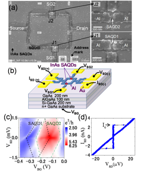
In order to characterize the QD properties, we measured a differential conductance (versus a source-drain voltage and a back-gate voltage ) under the magnetic field of 100 mT to suppress superconductivity and at =0 V (see Fig. 1(c)). Note that since the simultaneously changes the properties of two QDs (SAQD1 and SAQD2) which are parallelly connected in SQUID, Fig. 1(c) depicts the mixture of the Coulomb diamonds of two QDs. We mark simple guide lines for the Coulomb diamonds corresponding to odd occupation of each dot in the Fig. 1(c) where dot property for SAQD1 is distinguishable due to response (not shown). We roughly estimate the dot properties in SQUID to be a charging energy 1.7 meV and a level spacing 0.9 meV for SAQD1 while it is too vague to assign for SAQD2. The Coulomb oscillations with have been detected with the differential conductance ranging up to 6.25 . By changing , the conductance value of SAQD1 only is shifted with a value of less than 2 . Also the strong Kondo effect was observed for SAQD2 due to strong dot-lead coupling. We think that the high conductance over 6 is mainly contributed from SAQD2 being in open dot regime.
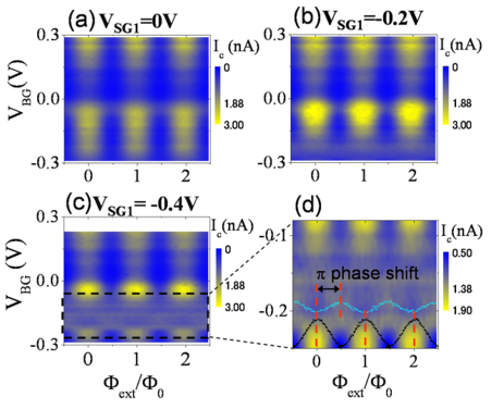
In an absence of any magnetic field, the characteristic of SQUID exhibits a clear supercurrent (with a critical value of =2.5 nA) with accompanying a hysteretic behavior as shown in fig. 1(d). As a function of external magnetic field (), the periodic oscillation is shown in Fig. 2(a) where the period of about =1.5 gauss is well consistent with the addition of a flux quantum to the effective SQUID area. This result implies that the loop including Al/SAQD/Al junctions operate as SQUID. For individual control of SAQD1, we additionally tuned to be -0.2 V (Fig. 2(b)) and -0.4 V (Fig. 2(c)). Interestingly we observed junction behavior for =-0.4 V which manifests as phase shift on oscillation at certain voltage regime of (see Fig. 2(d) which is enlarged graph of (c)). This means the presence of spontaneous supercurrent in the loop induced by control of and only one of SAQD junctions is in junction state while the other is so-called 0 junction.
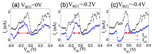
For more detailed study for -junction transition, we plot the individual profiles of each junction in Fig. 3 which is resultant from the analysis of the interference properties of SQUID in the limit of small self inductance as described below. This method is very useful when we want to know the individual properties for the QD-SQUID where more than one of junctions in the SQUID can not be (Coulomb) blockaded, for instance open dot case.
Due to a relatively small and small self inductance of about 15 pH calculated from SQUID geometry, the total of our device can be expressed as the following expression in the limit of small self inductance Barone:p371
| (1) |
where and are the critical currents of each junction, J1 and J2. According to Eq. (1), amplitude has maximum corresponding to + at = and minimum being - at =. Thus we can obtain from () -()/2 and also from ()-.
As shown in Fig. 3, we obtained only positive values for the which implies that the 0- junction transition does not occur in J2. Only for J1, we found a negative supercurrent at specific voltage range which corresponds to the region showing phase shift on oscillation in Fig. 2(d). Such supercurrent reversal has been demonstrated by adding a single electron to the QD Josephson junctions using carbon nanotubeCleuziou:2006 ; Jorgensen:2007 and InAs nanowire.Dam:2006 Also other mechanisms for negative supercurrent have been experimentally studied in d-wave high superconductor,Harlingen:1995 a superconductor/ferromagnet/superconductor,Ryazanov:2001 and a superconductor/normal metal/superconductor Josephson junction.Baselmans:1999
In our experiment, the is used to tune mainly the energy level in the quantum dots and the is for the change of coupling between QD1 and superconducting leads. In Fig. 3(a)-(c), the maxima are induced by the resonance between the energy levels in SAQD and the Fermi energy in the superconductor and the broadening of the peaks depends on the dot-lead coupling. One can notice that the peak widths of indicated by the arrows in Fig. 3 are changed by the . This fact implies that the SG1 controls the coupling energy. This is good agreement with Ref. Kanai:2010, where although there is no direct observation of -junction behavior, it shows the possibility of the phase transition between Kondo singlet and magnetic doublet ground states driven by the side-gate modulation of the device tunnel coupling.
In summary, we fabricated a SAQD-SQUID which is the first try in a sense of combination of the uncapped InAs SAQD with unique structural zero-dimensionality and SQUID. Using SQUID geometry, we directly observed the junction behavior accompanying negative supercurrent by tuning a side-gate. Our results support Ref.Kanai:2010, where the junction transition was explained by the singlet-doublet transition of the spin state of the InAs SAQD due to a change of the coupling between SAQD and superconducting leads by side-gate without direct observation of state. Employing InAs SAQD to QD-SQUID may open new possibility for a quantum information processing in a wide range of optics, spintronics, and superconductivity.
This research is supported by the Japan Society for the Promotion of Science(JSPS) through its FIRST program and Grant-in-Aid for Scientific Research(KAKENHI) S (No. 20221007). The author (S. Kim) would like to thank to R. Inoue and S. Moriyama for helpful discussions.
References
- (1) J. -P. Cleuziou, W. Wernsdorfer, V. Bouchiat, T. Ondarçuhu and M. Monthioux, Nature Nanotech. 1, 53 (2006).
- (2) J. A. van Dam, Y. V. Nazarov, E. P. A. M. Bakkers, S. D. Franceschi, and L. P. Kouwenhoven, Nature 442, 667 (2006).
- (3) M. Kroutvar, Y. Ducommun, D. Heiss, M. Bichler, D. Schuh, G. Abstreiter, and J. Finley, Nature 432, 81-84 (2004).
- (4) M. Jung. K. Hirakawa, Y. Kawaguchi, S. Komiyama, S. Ishida, and Y. Arakawa, Appl. Phys. Lett. 86, 033106 (2005).
- (5) C. Buizert, A. Oiwa, K. Shibata, K. Hirakawa, and S. Tarucha, Phys. Rev. Lett., 99, 136806 (2007).
- (6) R. S. Deacon, Y. Tanaka, A. Oiwa, R. Sakano, K. Yoshida, K. Shibata, K. Hirakawa, and S. Tarucha, Phys. Rev. Lett. 104, 076805 (2010).
- (7) K. Shibata, C. Buizert, A. Oiwa, K. Hirakawa, and S. Tarucha, Appl. Phys. Lett. 91, 112102 (2007).
- (8) A. B. Zorin, Rev. Sci. Instrum. 66, 4296 (1995).
- (9) A. Barone and G. Paterno, Physics and Applications of the Josephson Effect (A wiley-interscience publication, New York, 1982).
- (10) H. I. Jørgensen, T. Novotný, K. Grove-Rasmussen, K. Flensberg, and P. E. Lindelof, Nano Lett. 7, 2441 (2007).
- (11) D. J. van Harlingen, Rev. Mod. Phys. 67, 515 (1995).
- (12) V. V. Ryanov et al., Phys. Rev. Lett. 86, 2427 (2001).
- (13) J. J. A. Baselmans, A. F. Morpurgo, B. J. van Wees, and T. M. Klapwijk, Nature 397, 43 (1999).
- (14) Y. Kanai, et. al., Phys. Rev. B 82 054512 (2010).