Nanometer Structure Consortium, nmC@LU
Signatures of Wigner Localization in Epitaxially Grown Nanowires
Abstract
It was predicted by Wigner in 1934 that the electron gas will undergo a transition to a crystallized state when its density is very low. Whereas significant progress has been made towards the detection of electronic Wigner states, their clear and direct experimental verification still remains a challenge. Here we address signatures of Wigner molecule formation in the transport properties of InSb nanowire quantum dot systems, where a few electrons may form localized states depending on the size of the dot (i.e. the electron density). By a configuration interaction approach combined with an appropriate transport formalism, we are able to predict the transport properties of these systems, in excellent agreement with experimental data. We identify specific signatures of Wigner state formation, such as the strong suppression of the antiferromagnetic coupling, and are able to detect the onset of Wigner localization, both experimentally and theoretically, by studying different dot sizes.
pacs:
73.21.Hb, 73.22.Gk, 73.22.Lp, 73.23.Hk, 73.63.NmThe transition to a Wigner crystal Wigner (1934) can be viewed as a contest between the electronic Coulomb repulsion and the quantum mechanical kinetic energy. If the Coulomb repulsion dominates, the many-particle ground state and its excitations resemble a distribution of classical particles located in a lattice minimizing the Coulomb energy. In the bulk, the transition to a Wigner crystal is only expected for extremely dilute systems Ceperley and Alder (1980); Drummond et al. (2004), while in lower dimensions, or for broken translational invariance, it becomes accessible at higher densities Tanatar and Ceperley (1989); Jauregui et al. (1993); Rapisarda and Senatore (1996). A lot of work has focused on finite-sized two-dimensional quantum dots Creffield et al. (1999); Egger et al. (1999); Yannouleas and Landman (1999); Filinov et al. (2001); Reimann and Manninen (2002), where the crossover from liquid to localized states in the transport properties of the nanostructure has been addressed Cavaliere et al. (2009); Ellenberger et al. (2006). For one-dimensional systems, localization has been reported in cleaved edge overgrowth structures Auslaender et al. (2005) and for holes in carbon nanotubes Deshpande and Bockrath (2008). These highly correlated one-dimensional systems exhibit a variety of fascinating features as reviewed recently Deshpande et al. (2010). Here we introduce a third system, based on epitaxially grown semiconductor nanowires, which allows a straightforward application of tunneling spectroscopy compared to the rather involved cleaved edge overgrowth structures and avoids further complications due to the isospin degree of freedom in carbon nanotubes.
InSb nanowires Nilsson et al. (2009), as used here, allow for the realization of quantum dots, where the electronic confinement along the nanowire is established by Schottky barriers to gold contact stripes, see Fig. 1(a). Varying the distance between the stripes (here: 70 nm and 160 nm) allows for the systematic realization of wires with specific length and thereby controlled electron densities. For our calculations we model the nanowire as a hard-wall cylinder with the experimental radius 35 nm. The Schottky barrier at the semiconductor-metal interface creates a standard quantum well with a width equal to the contact spacing. The Coulomb interaction between the electrons is approximated as that in a cylinder embedded in homogeneous matter, taking into account the different dielectric constants of the wire and the surrounding material Slachmuylders et al. (2006); Li et al. (2008). Exact many-particle states in the wire are evaluated with the configuration interaction method.
The results can be understood in terms of two limiting cases: a short wire with no electron localization and a long wire with Wigner localization111As we focus on 2-3 electrons, we cannot speak of a macroscopic effect such as Wigner crystallization. Hence the term Wigner localization..
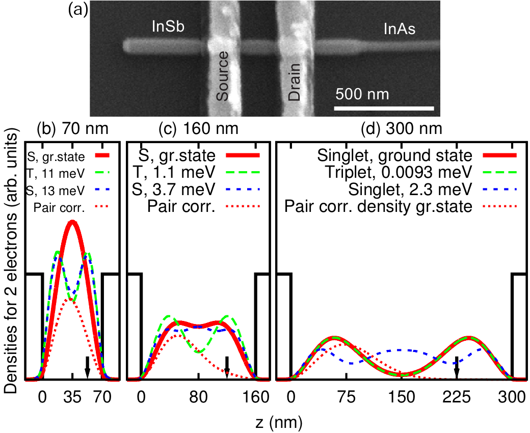
The first limiting case, where interaction is dominated by kinetic energy, can be described by the independent-particle shell model. There the two-particle ground state is obtained by populating the lowest single-particle level with a spin-up and a spin-down electron. Thus the spatial electron density follows that of the lowest single-particle level and exhibits a peak in the center of the quantum dot. The lowest excited two-particle state is obtained by moving one electron to the first excited single-particle level at the cost of the level spacing energy . Thus one expects the two-particle excitation energy . Furthermore the spin degrees allow for four realizations of such an excited two-particle state, which are typically split into a triplet and a singlet due to exchange interaction.
In the second limiting case, Wigner localization, the electrons are localized at different positions along the wire, minimizing the Coulomb repulsion. Thus the two-particle ground state density exhibits two peaks and a minimum in the center of the nanowire segment. As the electrons can have arbitrary spin on each site, one has four realizations of this configuration, with a minor energy split between a singlet and a triplet. Hence, we expect a very small , while further excitations are significantly higher in energy and exhibit a different spatial distribution of charge.
At the onset of localization, the electron density is expected to resemble two weakly separated peaks in the two-particle ground state. The interaction of the electrons is substantial, without yet dominating the kinetic part. Hence the two-particle excitation energy is considerably lower than the single-particle excitation energy, . However, as the two electrons are not yet fully crystallized, is expected to be well above zero.
Tunneling spectroscopy is a convenient way to study ground and excited states in quantum dot systems. Here we can use the gold contacts (Fig. 1(a)) as source and drain by applying a bias between both stripes. The nanowire is located on a highly doped Si substrate covered by an insulating SiO2 layer, which allows for application of a back-gate voltage providing an approximately homogeneous shift in energy of all levels in the dot. Varying and provides the characteristic charging diagrams (see e.g. Reimann and Manninen (2002)) displayed in Figs. 2(c) and 3(c) at a temperature of 300 mK. Here high differential conductance indicates that the electron addition energy (affinity) coincides with the chemical potential in either of the gates. The diamonds of vanishing conductance centered around zero are the regions of Coulomb blockade, where the chemical potentials of both reservoirs are above the energy difference between the - and -electron ground state and below the energy difference between the - and -electron ground state. As no further lines of high conductance are found for lower gate bias, we assume that the lowest diamond corresponds to . Half the width of this diamond defines the charging energy .
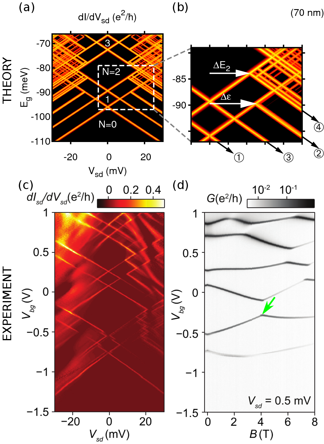
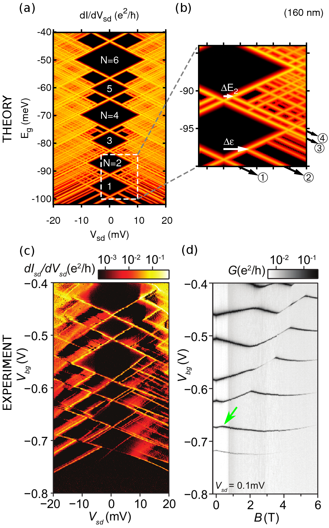
Based on the calculated many-particle states, electron transport is treated within the master equation model Chen et al. (1994); Kinaret et al. (1992); Pfannkuche and Ulloa (1995) with tunneling matrix elements calculated as in Ref. Cavaliere et al. (2009). The results are displayed in Figs. 2(a) and 3(a) for the respective experimental samples displayed in panel (c). We find that all Coulomb diamonds agree rather well, which indicates that the radial excitations, which are disregarded in our effectively one-dimensional model, only become of relevance for higher particle numbers in the dot.
Now we focus on the excited states and show, that the experimental conductance data along with our theoretical calculations allow for a verification of the Wigner localization scenario described above.
For a 70 nm wire, the 2-electron density along the wire is a single peak, see Fig. 1(b). This corresponds to the independent-particle shell model as described above. In Fig. 2(b) we have marked the lines, where the first electron enters the one-electron ground state and the one-electron excited state, by the symbols ➀ and ➁, respectively. This reflects the level spacing meV as shown by the horizontal arrow. Similarly, starting from the one-electron ground state, the second electron enters the dot reaching the two-electron ground state and the two-electron excited state at lines marked by the ➂ and ➃ symbols. The separation between these two lines represents the excitation energy meV. The four lines, ➀-➃, can be observed in the experimental data in Fig. 2(c) (this is clearer for negative bias, as the measurement results in the positive bias region most likely suffer from charging of impurity states). From this figure, we read , and hence for the sample of length 70 nm, the experimental data are in good agreement with the independent-particle shell model discussed above.
Note that there is some discrepancy between theory and experiment regarding the value of and . This could be due to bending of energy levels at the interface of the wire and the gold contacts (Schottky barriers), which makes the wire effectively shorter than the spacing of the contacts. Indeed, simulations of a 60 nm wire give meV and meV.
We can quantify the electron-electron interaction strength by the energy difference between the two-particle ground state and twice the energy of the lowest single-particle level (half-width of the Coulomb diamond). This provides the charging energy meV for the 70 nm sample, as read from Fig. 2(c). That is , in accordance with the independent-particle shell model being valid when kinetic energy dominates interaction.
For the 160 nm wire, the 2-electron density in Fig. 1(c) resembles two semi-separated peaks, indicating the onset of Wigner localization (as also seen in the pair-correlated density). In Fig. 3, the lines ➀-➃ can be identified both in the simulation and the experiment. The theoretical results give meV and meV, as in the experiments we observe . Again, this is in agreement with the scenario of onset of Wigner localization discussed above.
Note that if we would neglect the different dielectric consant outside the wire, the onset of Wigner localization would first appear at double the actual wire length. Hence the screening due to the different dielectric constants of the wire and the surrounding material is an important effect and must be included in the modelling.
The energy separation between the singlet and the triplet two-electron state, the antiferromagnetic coupling, can also be manifested by the magnetic field dependence of the differential conductance. The part of the triplet is lowered in energy by a magnetic field with respect to the singlet state by , where is the Bohr magneton. Fig. 3(d) shows that there is a level crossing at T (marked by an arrow). According to Ref. Nilsson et al. (2009) the electronic -factors are around 40 for two electrons in the dot. This provides an energy splitting meV in full agreement with the calculated value for the 160 nm wire. Note that for the 70 nm wire, the level splitting is no longer linear in the high magnetic field, T, at which the crossing appears (marked by an arrow in Fig. 2(d)). Hence we cannot apply the same method to find for the 70 nm wire, although its result meV is of the correct order of magnitude. The strong suppression of this antiferromagnetic coupling between the two electrons (by an order of magnitude, while changing the length by about a factor of two) is one of the hallmarks of the Wigner crystal state Deshpande et al. (2010).
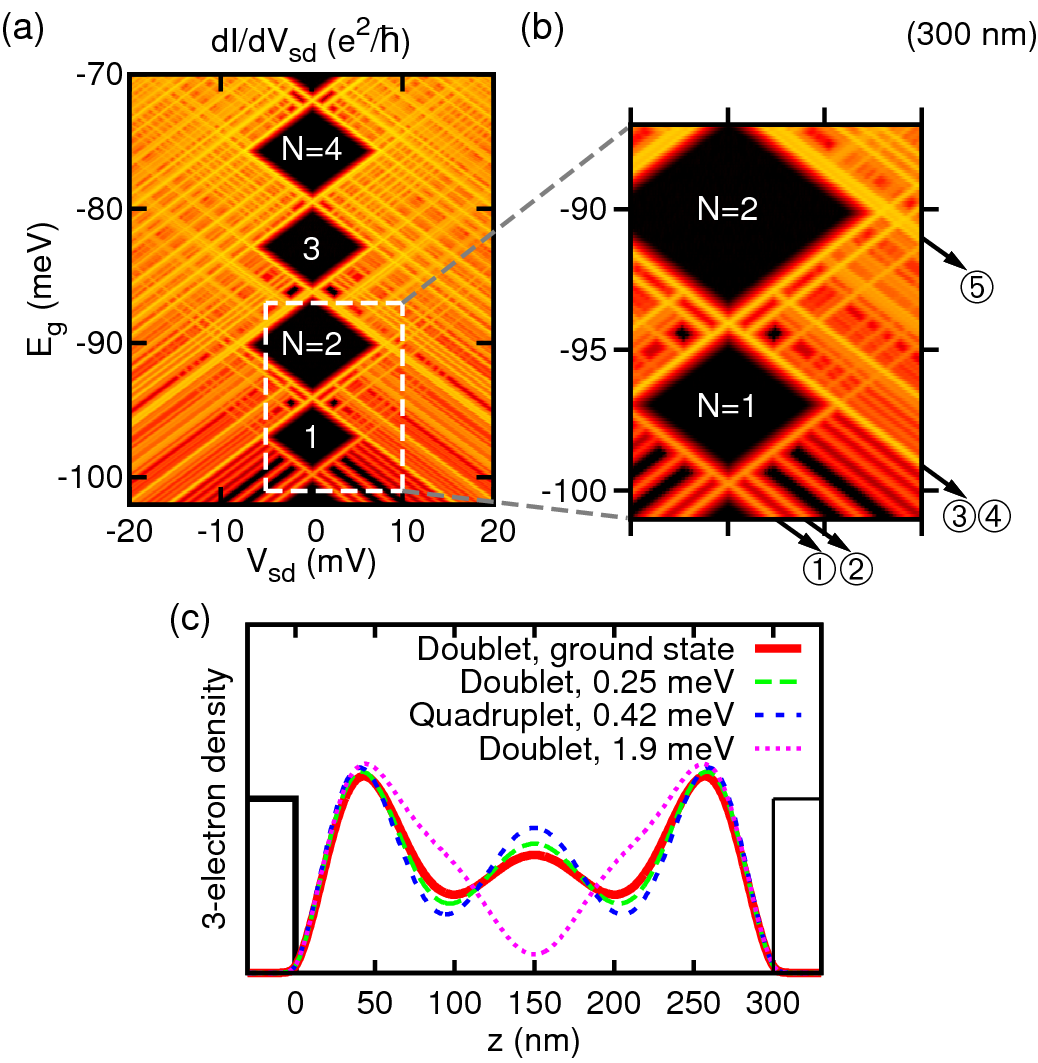
Finally, our theoretical results indicate complete Wigner localization for a 300 nm long wire. Fig. 1(d) shows that in the two-particle ground state, the electrons are strongly localized, i.e. they form a Wigner molecule. From Fig. 4(b) we observe that the conductance line of the triplet first excited state (➂) has merged into the line of the singlet ground state (➃), as expected: There is no difference in the energy of these two states, as there should be no difference between the singlet and triplet states of two strongly localized particles. More precisely we find eV and meV, i.e. . Furthermore we find meV, that is . This conforms to Wigner localization being present when kinetic energy is strongly dominated by interaction.
Even for the ground state the theoretical calculations suggest the onset of Wigner localization in a 300 nm wire, as seen in Fig. 4(c). The small energy difference between the three lowest states results in a broad conduction line, marked by the symbol ➄ in Fig. 4(b). Unfortunately, we could not obtain experimental data for this length, since for such a long sample and low charge densities the effect of disorder is too strong, creating an effective double quantum dot. This can be identified in a charge stability diagram as additional kinks in the conductance lines that comprise the Coulomb diamond Fuhrer et al. (2007). Such kinks are not present in the stability diagram for the 160 nm wire shown in Fig. 3(c), implying that disorder has no significant effect in that case. Also, Coulomb interaction has been shown to decrease the effect of Anderson localization Filinov et al. (2002). However the theoretical results demonstrate the prospects of our approach, if more efficient gating schemes are developed.
We have demonstrated the transition from the independent-particle shell model to Wigner localization with increasing length of a semiconductor nanowire sample. While the excitation spectrum follows the independent-particle shell model for the 70 nm wire (), the onset of Wigner localization is observed for the 160 nm wire () and finally our simulations show complete Wigner localization in a wire of length 300 nm. There the excitation energy of the two-particle state is almost negligible and much lower than the level spacing, , and the calculated electron density exhibits two peaks. This shows that InSb nanowires form a convenient system to investigate strongly correlated systems by well established transport measurement techniques.
This work was supported by the Swedish Research Council (VR) as well as the Swedish Foundation for Strategic Research (SSF).
References
- Wigner (1934) E. Wigner, Phys. Rev 46, 1002 (1934).
- Ceperley and Alder (1980) D. M. Ceperley and B. J. Alder, Phys. Rev. Lett. 45, 566 (1980).
- Drummond et al. (2004) N. D. Drummond, Z. Radnai, J. R. Trail, M. D. Towler, and R. J. Needs, Phys. Rev. B 69, 085116 (2004).
- Tanatar and Ceperley (1989) B. Tanatar and D. M. Ceperley, Phys. Rev. B 39, 5005 (1989).
- Jauregui et al. (1993) K. Jauregui, W. Häusler, and B. Kramer, EPL 24, 581 (1993).
- Rapisarda and Senatore (1996) F. Rapisarda and G. Senatore, Aust. J. Phys 49, 161 (1996).
- Creffield et al. (1999) C. E. Creffield, W. Häusler, J. H. Jefferson, and S. Sarkar, Phys. Rev. B 59, 10719 (1999).
- Egger et al. (1999) R. Egger, W. Häusler, C. H. Mak, and H. Grabert, Phys. Rev. Lett. 82, 3320 (1999).
- Yannouleas and Landman (1999) C. Yannouleas and U. Landman, Phys. Rev. Lett. 82, 5325 (1999).
- Filinov et al. (2001) A. V. Filinov, M. Bonitz, and Y. E. Lozovik, Phys. Rev. Lett. 86, 3851 (2001).
- Reimann and Manninen (2002) S. Reimann and M. Manninen, Rev. Mod. Phys. 74, 1283 (2002).
- Cavaliere et al. (2009) F. Cavaliere, U. D. Giovannini, M. Sassetti, and B. Kramer, New Journal of Physics 11, 123004 (2009).
- Ellenberger et al. (2006) C. Ellenberger, T. Ihn, C. Yannouleas, U. Landman, K. Ensslin, D. Driscoll, and A. C. Gossard, Phys. Rev. Lett. 96, 126806 (2006).
- Auslaender et al. (2005) O. M. Auslaender, H. Steinberg, A. Yacoby, Y. Tserkovnyak, B. I. Halperin, K. W. Baldwin, L. N. Pfeiffer, and K. W. West, Science (New York, N.Y.) 308, 88 (2005).
- Deshpande and Bockrath (2008) V. Deshpande and M. Bockrath, Nat. Phys. 4, 314 (2008).
- Deshpande et al. (2010) V. V. Deshpande, M. Bockrath, L. I. Glazman, and A. Yacoby, Nature 464, 209 (2010).
- Nilsson et al. (2009) H. A. Nilsson, P. Caroff, C. Thelander, M. Larsson, J. B. Wagner, L.-E. Wernersson, L. Samuelson, and H. Q. Xu, Nano Lett. 9, 3151 (2009).
- Slachmuylders et al. (2006) A. F. Slachmuylders, B. Partoens, W. Magnus, and F. M. Peeters, Phys. Rev. B 74, 235321 (2006).
- Li et al. (2008) B. Li, A. F. Slachmuylders, B. Partoens, W. Magnus, and F. M. Peeters, Phys. Rev. B 77, 115335 (2008).
- Chen et al. (1994) G. Chen, G. Klimeck, S. Datta, G. Chen, and W. A. Goddard III, Phys. Rev. B 50, 8035 (1994).
- Kinaret et al. (1992) J. M. Kinaret, Y. Meir, N. S. Wingreen, P. A. Lee, and X.-G. Wen, Phys. Rev. B 46, 4681 (1992).
- Pfannkuche and Ulloa (1995) D. Pfannkuche and S. E. Ulloa, Phys. Rev. Lett. 74, 1194 (1995).
- Fuhrer et al. (2007) A. Fuhrer, L. E. Fröberg, J. N. Pedersen, M. W. Larsson, A. Wacker, M.-E. Pistol, and L. Samuelson, Nano Letters 7, 243 (2007).
- Filinov et al. (2002) V. Filinov, P. Thomas, I. Varga, T. Meier, M. Bonitz, V. Fortov, and S. W. Koch, Phys. Rev. B 65, 165124 (2002).