Huge enhancement of the magnetoresistance and negative differential conductance in nanostructure arrays
Abstract
We show that the interplay between charging effects and the non-equilibrium spin accumulation has a dramatic effect in the current through an array of nanostructures attached to ferromagnetic electrodes. Large oscillations in the current as a function of bias voltage show up for parallel orientation of the electrodes’ magnetizations. These oscillations originate in the inhomogeneity of the spin potentials through the array and correlate with oscillations in the spin accumulation. For antiparallel orientation the spin potential is homogeneous and the oscillations do not show up. This sensitivity results in a huge enhancement of the tunneling magnetoresistance as compared to the single-island case, and open new routes for improving the spintronic response of nanodevices.
A lot of effort has been devoted in the last two decades to understanding and controlling the interplay between magnetism and charge current because of promising applications in electronic devicesreviewawschalom ; reviewjohnson ; reviewfert ; spintronics . Interest is focused on systems with a large magnetoresistance (MR), defined in terms of the resistance of the device for parallel (P) and antiparallel (AP) orientation of two ferromagnetic electrodes, . The tunneling magnetoresistance (TMR) of magnetic tunnel junctions, early studied by Julliérejulliere , is controlled by the spin polarization of the carriers , assumed here to be equal in both electrodes:
| (1) |
In a magnetic double tunnel junction, with a metallic area inserted between the ferromagnetic electrodes, the TMR vanishes except if the spin flip processes are of little importance in the metal. Otherwise, the tunneling electrons lose memory of their initial spin. When the spin relaxation time is long, spin accumulation happens and induces a spin splitting of the chemical potential in the antiparallel configurationjohnsonprl . The TMR is finite but only the half of Julliere’s value. A further reduction of the magnetoresistance occurs with increasing number of metallic non-magnetic insertions, , separated among themselves by tunnel barries:
| (2) |
where all the tunnel barriers separating the metallic insertions are supposed to be equivalent. The reduction of the TMR with the number of metallic regions is expected as it is only via the spin accumulation that the information about the relative magnetic orientation of the electrodes is transferred. This mechanism is indirect and less effective than the direct coupling of the two electrodes in a single tunnel junctionweymann2005 .
If the dimensions of the metallic insertion are reduced charging effects can no longer be neglected and new phenomena appear in the currentcb and in the magnetoresistanceono97 . Due to the cost in energy to add an electron to the islands, at zero temperature, the current is blocked below a threshold voltage . For a symmetrically biased array with nonmagnetic electrodes and short-range interactions nosotrosprb08 . Above this threshold the current is non-linear in voltage and frequently shows Coulomb staircase features. For a single island, a finite polarization of the electrodes can induce regions of negative differential conductance, as well as oscillations and changes of sign in the TMR, dependending on the specific set-up barnas98 ; maekawa98 ; barnasepl ; brataas99 ; imamura99 ; yakushiji2005 . Charging effects are known to be enhanced in nanostructure arrayscb ; likharev89 ; middleton93 ; nosotrosprb08 , however little is known about the spin transport in these systems. As the spin accumulation is the only way to transfer the spin information, a reduction of the TMR with increasing number of islands, similar to that in Eq.(2) could be expected, a priori.
Here we show that, increasing the number of islands in between two ferromagnetic electrodes has a dramatic impact on the charge and spin transport. Large current oscillations show up in the I-V curves for parallel magnetic orientation, resulting in a strongly voltage dependent tunneling magnetoresistance. This behavior is a consequence of the interplay between charging effects and the spin accumulation through the array. The latter is homogenous along the array in the antiparallel configuration while it is inhomogenous and changes sign for parallel orientation. Opposite to what happens in the absence of charging effects, the TMR can be orders of magnitude larger than in the single particle case.
We consider an array of metallic nanostructures, in the following called islands, with charging energy and single particle level spacing satisfying . is the temperature and the Boltzmann constant. To allow for spin accumulation is kept finite. The array is placed in between two ferromagnetic electrodes with spin polarization . The islands are separated between themselves and from the ferromagnetic electrodes by equivalent tunnel junctions. The electronic interactions are assumed to be finite only when the charges are in the same conductor i.e. capacitive coupling between different conductors vanishes, and charge disorder is absent. The electronic charge is taken equal to unity. Transport is treated at the sequential tunneling level with tunneling rates
| (3) |
Here is the change in energy of electrons with spin due to the tunneling process. The ferromagnetic polarization of the electrodes enters via the tunneling resistance. is equal to at the internal junctions separating two islands and to at the contact junctions between an electrode and the neighboring island. Plus (minor) signs are assigned to majority (minority) spin carriers. The spin is conserved in the tunneling and in between tunneling events. Magneto-Coulombono97 ; vandermolen06 ; kouwenhoven09 , spin-orbit effects, and the role of the metal insulator interfacedeteresa99 in determining the spin polarization of the carriers are neglected through all the paper.
Under these assumptions the spin dependent potential at island is with running from to and the number of excess electrons with spin at island . Correspondingly the spin accumulation at island is given by . The electrodes are maintained at spin-independent potentials and and current flows perpendicular to the array axis.
To calculate the current we use a Monte Carlo simulation which depends on the tunneling rates, as described in previous workslikharev89 ; nosotrosprb08 . At each iteration a single tunneling event takes place. The time involved in this event depends on the tunneling rates of all the possible tunneling processes. These rates are calculated at each iteration as they change when the spin and charge state of the system does. The values of the current given here correspond to stationary states. This computational method is appropriate for low temperatures when the electrons flow in the same direction in all the relevant tunneling processes. With increasing temperature the electrons become frequently stacked, oscillating back and forth between two islands and computation is not possible. Calculations reported here correspond to , and with energies given through all the paper in units of . The value of does not affect the results as far as is satisfied. The non-zero temperature used to ensure allows a very small but finite current below threshold values. For simplicity, in most part of the discussion this finite temperature effect is neglected.
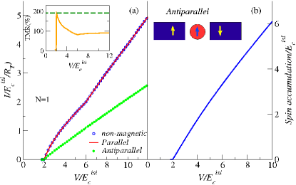
Results for a single island are shown in Fig. 1. For parallel arrangement the current can be described in terms of two independent spin channels and has the same value found with nonmagnetic electrodes, see Fig. 1a. For antiparallel orientation spin accumulation appears to equalize the ratios for entrance and exit from the island of spin up and down electrons, see inset in Fig. 1b. Both the current and the spin accumulation increase monotonously with voltage above as shown in Fig. 1. The inset in Fig. 1a shows the TMR corresponding to a single island as a function of the bias voltage . When charging effects are not important and the TMR equals half of Julliere’s value, as expected for a double tunnel junction. As the voltage is reduced the TMR first decreases slightly and then increases until where it suddenly jumps to zero. The maximum TMR, found at equals Julliere’s value given in Eq. (1).
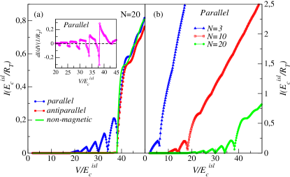
A very different behavior is found for , as the inner junctions between the islands can block the current flow. In the antiparallel configuration, as for non-magnetic electrodes, the current is strongly suppressed below where a large jump is observed, see Figure 2(a). Surprisingly for parallel orientation of the electrode magnetization the current show large oscillations below . Within the range of voltages at which these oscillations are observed, there are regions in which the current decreases with increasing , corresponding to negative differential conductance. This negative conductance can be quite large, see the inset of Fig. 2 (a). As observed in Figure 2(b), the number of peaks observable in the current increases with the number of islands in the array.
This unexpected behavior can be understood from an analysis of the potential drop through the array. In the case of metallic non-magnetic electrodes, the large threshold voltage originates in the lack of potential drop at the inner junctions which impede the flow of charges below . This situation is typical of short-range interactions, as the voltage drops mostly at the junctions adjacent to source and drain, see discussion in nosotrosprb08 . With increasing voltage charges are allowed to enter the array from the electrodes and create a charge gradient which provides the potential drops at the inner junctions necessary to allow the tunneling processes. Once a single charge occupies the first island, to increase the number of charges on it a voltage rise equal to is needed. is the voltage necessary to put around charges onto the first island (the exact number depends on being even or odd).
Because of the spin accumulation when the electrodes are magnetic the potential profile is spin dependent. In the antiparallel configuration the spin-up and spin-down potentials change only very slightly when moving from an island to its neighboring ones, see Fig. 3(a). The spin accumulation is very homogeneous through the array. So, it barely contributes to the change in energy for tunneling at the inner junctions. As for non magnetic electrodes, this change in energy is controlled by the charge gradient at the junctions. The position dependence of the spin accumulation is very different in the antiparallel and parallel cases, see the sketches given at the top of Figure 3. For parallel orientation of the electrodes magnetization the spin accumulation changes sign as one moves from the first island to the end of the array, as seen in Fig. 3(b), where we plot the spin potentials corresponding to and as a function of the island position. Spin down (up) potential increases (decreases) producing potential drops at the junctions between the islands which oppose (favor) the current flow. Because of this potential drop created by the spin accumulation the charge gradient needed to allow the flow of spin up electrons decreases. With the reduction of the number of charges which have to be accumulated at the first or last island to allow current, the threshold voltage is reduced. Current is observed at smaller voltages for parallel arrangement of the electrode magnetizations than in the antiparallel or nonmagnetic cases. With the potential drop at the inner junctions being spin dependent, naively one could expect a complete spin polarization of the current. As observed in Fig. 3(c), this does not happen. The current polarization is not complete because the flow of spin-down electrons is allowed via the charge potential left by the spin-up ones.
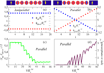
If, as discussed above, the current flows thanks to the spin accumulation, one could expect a decrease in the latter correlated with the regions of negative differential conductance. This is confirmed in Fig. 3(d) which shows oscillations in the spin accumulation at the same voltages as in the current. The decrease in the spin accumulation is due to the opening of a new transport channel only for spin down electrons. This is possible because the voltage drop necessary to permit the entrance of spin-down charges at the first island is smaller than the one corresponding to spin-up ones. At some , being the first island occupied with charges, spin-down electrons would be allowed to enter, while spin-up electrons will not. As spin accumulation happens to equilibrate the ratio between entrance and exit of spin up and down electrons, the opening of a new conduction channel for down electrons will reduce the spin accumulation. This is the origin of the decrease of current with increasing voltage, which lasts until this conduction channel is also opened for spin-up electrons.
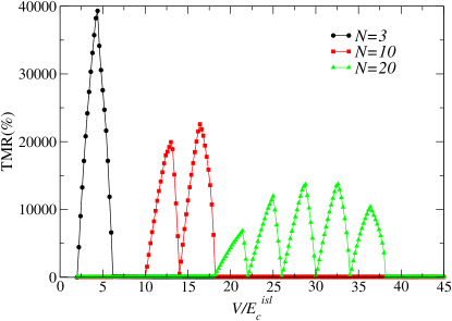
The differences in the current as a function of a magnetic orientation have a dramatic effect on the TMR, plotted in Figure 4, which is strongly voltage dependent. Like the current it shows peaks in the parallel configuration. But the most impressive result are the extremely large values of the TMR observed. Even more than two orders of magnitude larger than in the single island case and than the value predicted by Eq. (2) which is recovered at large voltages (not shown). The largest values of the magnetoresistance depend on voltage and are largest for . This shows that there is a lot of room to improve the TMR response of electronic devices.
In summary, we have studied the interplay between magnetism and charging effects in the transport through nanostructure arrays placed between ferromagnetic electrodes. We have found very non-linear I-V curves for parallel orientation of source and drain magnetizations, which include peaks in the current at voltages smaller than the metallic threshold voltage. This unusual dependence originates in the inhomogeneity of the spin potential through the array. The oscillations of the current correlate with oscillations of the TMR and of the spin accumulation which changes sign through the array. The TMR can reach values two orders of magnitude larger than those found in the single island case. Our results show that in the presence of charging effects a proper patterning can largely enhance the value of the magnetoresistance and will stimulate further experimental and theoretical studies.
We are thankful to J. König for proposing us this analysis and for enlightening discussions. V. Estévez thanks the hospitality of the University of Duisburg-Essen where this work was initiated. Funding from Ministerio de Ciencia e Innovación through Grants No. FIS2008-00124/FIS, FPI fellowship and Ramón y Cajal contract, and from Consejería de Educación de la Comunidad Autónoma de Madrid and CSIC through Grants No. CCG07-CSIC/ESP-2323, CCG08-CSIC/ESP3518, PIE-200960I033 is acknowledged.
References
- (1) S.A. Wolf, D.D. Awschalom, R.A. Buhrman, J.M. Daughton, S. von Molnár, M.L. Roukes, A.Y. Chtchelkanova and D.M. Treger. Science 294, 1488 (2001).
- (2) M. Johnson. J. Phys. Chem. B 109, 14278 (2005).
- (3) C. Chappert, A. Fert, A. Van Dau and F. Nguyen. Nat. mat. 6, 813 (2007).
- (4) S. Bandyopadhyay and M. Cahay, Introduction to Spintronics, ed. CRC Press, New York (2008).
- (5) M. Julliére. Phys. Lett. A, 54, 225 (1975).
- (6) M. Johnson and R.H. Silsbee, Phys. Rev. Lett. 55, 1790 (1985).
- (7) I. Weymann, J. König, J. Martinek, J. Barnás and G. Schön. Phys. Rev. B 72, 115334 (2005).
- (8) Single Charge Tunneling, NATO Advanced Studies Institute, Series B: Physics, edited by H. Grabert and M. H. Devoret (Plenum, New York) (1992).
- (9) K. Ono, H. Shimada and Y. Ootuka. J. Phys. Soc. Jpn. 66, 1261 (1997).
- (10) J. Barnás and A. Fert, Phys. Rev. Lett. 80, 1058 (1998).
- (11) S. Takahashi and S. Maekawa, Phys. Rev. Lett. 80, 1758 (1998).
- (12) J. Barnás and A. Fert. Europhys. Lett. 44, 85 (1998).
- (13) A. Brataas, Y. V. Nazarov, J. Inoue and G.E.W. Bauer, Phys. Rev. B 59, 93 (1999).
- (14) H. Imamura, S. Takahashi and S. Maekawa, Phys. Rev. B 59, 6017 (1999).
- (15) K. Yakushiji, F. Ernult, H. Imamura, K. Yamane, S. Mitani, K. Takanashi, S. Takahashi, S. Maekawa and H. Fujimori. Nat. Mat. 4, 57 (2005).
- (16) N.S. Bakhalov, G.S. Kazacha, K.K. Likharev and S.I. Serdyukova. Sov. Phys. JETP, 68, 581 (1989).
- (17) A.A. Middleton and N.S. Wingreen. Phys. Rev. Lett. 71, 3198 (1993).
- (18) E. Bascones, V. Estévez, J.A. Trinidad, and A.H. MacDonald, Phys. Rev. B 77, 245422 (2008).
- (19) S.J. van der Molen, N. Tombros and B.J. van Wees. 73, 220406 (2006).
- (20) F.A. Zwanenburg, D.W. van der Mast, H.B. Heersche, and L.P. Kouwenhoven. Nano Lett. 9, 2704 (2009).
- (21) J.M. De Teresa, A. Barthélémy, A. Fert, J.P. Contour, F. Montaigne, and P. Seneor. Magnetic Tunnel Junctions. Science 286, 507 (1999).