Giant mesoscopic spin Hall effect on surface of topological insulator
Abstract
We study mesoscopic spin Hall effect on the surface of topological insulator with a step-function potential. The giant spin polarization induced by a transverse electric current is derived analytically by using McMillan method in the ballistic transport limit, which oscillates across the potential boundary with no confinement from the potential barrier due to the Klein paradox, and should be observable in spin resolved scanning tunneling microscope.
Topological insulator (TI) with time reversal invariance has recently been proposed theoretically and observed in experimentskane1 ; sczhang1 ; sczhangrev ; kanerev ; moore ; hasan1 ; hasan2 ; xue ; fang . In three spatial dimensional (3D) TI, electronic structure is characterized by a bulk gap and a gapless surface mode described by odd number of branches of Dirac particles, which is protected by time reversal symmetry. The surface states are helical, where spins are locked with momentum. The gapless Dirac dispersion mode of the surface states has been confirmed in angle resolved photoemission spectroscope, and the predicted spin-momentum correlation has also been reported in experimentshasan1 ; hasan2 . Because of the strong correlation between the spin and momentum, the surface states of 3D TI may be a potentially idea system to study spintronics, where the electron’s spin degree is used to manipulate and to control mesoscopic electronic devices. It is interesting to note that the recent progress in TI is closely related to the development of the spin Hall effect (SHE) in the past several years, a sub-topic in spintronics.
The SHE refers to a boundary (surface or edge) spin polarization when an electric current is flowing through the system. There have been extensive studies on the SHE in the conventional semiconductors or metals with spin-orbit coupling, both in experimentkato ; sih ; wunderlich ; valenzuela and in theoryhirsch ; sfzhang ; engel ; tse ; murakami ; sinova . The SHE is often classified into ”extrinsic” (impurity driven) or ”intrinsic” (band structure driven). Since arbitrarily weak disorder destroys the intrinsic SHE in 2D infinite system with linear spin-orbit couplingmurakami2 ; engel2 , there have been considerable interests on the mesoscopic systems in the ballistic limit, where the disorder may be ignored nikolic ; zyuzin ; usaj ; jyao ; yxing ; bokes . In the ballistic limit, the electric field is absent inside the system, and the spin polarization is resulted from spin precession around the lateral confined potential. The SHE of 2D semiconductor system in the ballistic limit has been studied theoreticallyzyuzin ; usaj ; yxing . While the ballistic spin accumulation is predicted near the potential barrier, the effect has not been observed in experiments for the weakness of the effect in realistic semiconductors or for the difficulties to detect the spatial distribution of the spin polarization in the sandwiched interface. The surface states of the TI represent a different type of 2D system where the spin-orbit coupling is strong, and the surface state can be probed directly by scanning tunneling microscope (STM). This may provide a new route in study of the SHEsilvestrov ; sqshen and spintronics in general.
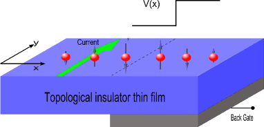
In this work, we report theoretical prediction of a giant SHE on a surface of 3D TI with a step-function potential in the ballistic limit as schematically illustrated in Fig. 1. By using McMillan Green function method, we derive analytic expressions for the electric current-induced spin polarization, which is oscillating across the potential boundary, and is not confined by the potential due to the Klein paradox. For a typical TI, the amplitude of the local spin polarization is estimated to be as large as at the Fermi level near the boundary, which is much larger than the SHE in a typical 2D semiconductor system, and should be observable in spin resolved STM experiments.
We consider surface states of TI, described by an effective Hamiltonian in the x-y plane,
| (1) |
where is the electron momentum, are the Pauli matrices, and is the Fermi velocity. The system is translational invariant along the y-axis, and has a step-function potential at , which separates two regions along the x-axis: region 1 at and region 2 at , as illustrated in Fig. 1,
where is a constant. A voltage of is applied across the surface to induce an electric current along the -direction. We consider the ballistic limit, where the electric field inside the surface is zero. We will first construct the retarded Green’s function by using the scattering wavefunction, a method introduced by McMillan to study superconducting state. From the obtained Green functions, we calculate the local spin density in the presence of the electric current to show the profound SHE. The experimental consequences and comparisons with the SHE in conventional 2D semiconductors will be discussed.
The scattering wave functions can be constructed based on the eigen functions of the Dirac particle in Hamiltonian (1) in the two separate spatial regions. The eigen wavefucntions in region corresponding to the energy and y-component momentum are given by
| (2) |
where . By adjusting the gate potential relative to the Fermi energy , the Dirac fermion carriers in region can be tuned into electron-like (-type, ) or hole-like (-type, ). Therefore the system may be viewed as or types of junction.
The right () and left () moving scattering wavefunctions can then be found by using the standard transfer matrix method. For a junction, we have
| (5) | |||||
| (8) |
where and are the transmission and reflection coefficients respectively, which are related by
| (17) |
where is the transfer matrix,
The scattering wavefunctions for a junction have similar form with that for the junction, except that are replaced by in the region of for the group velocity of a hole is opposite to that of an electron and that all the superindices of are replaced by .
We note that if is complex, the evanescent wave appears. In this case, considering the asymptotic behavior of the evanescent wave, the scattering wave function for both and junction will have the form given in Eqn. (5).
We are interested in the transverse effect of the charge and spin density profiles as an electric voltage is applied along the y-axis. To this end we construct the retarded Green’s function, which satisfies the equation,
| (18) |
where is a 2 by 2 identity matrix. The solution for is a direct product mcmillan of the scattering wavefunctions and the transposal wavefunctions ,
| (19) |
where and are the coefficients, which can be determined from Eqn. (4). Here, has the same form as , expect the replacement of the factor by .
The local spin density of states for a giving () and the local charge density of states at energy can be found easily from ,
| (20) |
where the sum in is over all the possible values of , and the contributions from the evanescent waves are also included.
In the present case, the Green’s function, hence the local charge and spin density of states can all be solved analytically. Here we shall focus on the spin z-component, which is most interesting and given by
| (22) | |||||
where is Heaviside function and . The charge density of states is directly related to the trace of ,
| (23) |
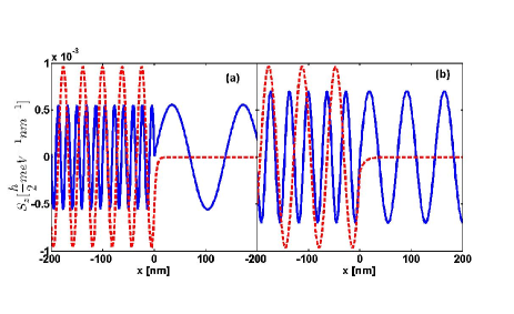
The local spin density of states for a giving in the and junctions are plotted in Fig.2. One important feature is the non-confinement of the Dirac particle with the higher barrier potential () due to the Klein paradox. The local spin density strongly depends on the incident angle of the electron, as we can see from Fig. 2. The evanescent wave appears if , and there is a critical incident angle for the condition of the evanescent wave. These features are typical characteristics of Dirac fermion, essentially the same as in the graphene.
We now calculate the spin polarization along x-direction near the potential boundary induced by an electric current along the y-direction at zero temperature. We consider a voltage of at the one edge and at the other edge of the system along the y-axis, and consider the ballistic transport limit. The effect of the voltage at the two edges is to induce an imbalance of the occupied states between and . The states with are occupied at energies below , and the states with are occupied at energies below , with the Fermi energy at . By the time reversal symmetry, the local spin polarizations contributed from and from with the same energy cancel to each other. For small value of , we thus obtain the current-induced net spin density profilezyuzin ; usaj ; datta
| (24) |
To further analyze the current-induced spin polarization, we define local spin susceptibility and local spin polarization ,
| (25) |
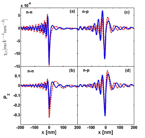
The local spin polarization is a dimensionless parameter to measure the magnitude of the SHE. means the spins of the electrons at a space point at the Fermi level are polarized. The experimentally measured local spin density is obtained by multiplying by the applied voltage and by the local density of states. In Fig.3 we plot and the in both and junctions. The key features of the SHE in the system are summarized below. 1). There is a pronounced oscillation of spin polarization near the potenial boundary . The peak value of is order of , and the peak value of is about , indicating the SHE here is giant. 2). The induced spin polarization is found to be insensitive to the Fermi energy on the TI surface. This may be understood because the spin polarization is approximately inversely proportional to , and is a constant for Dirac particles. This is markedly different from the usual 2D system where is proportional to , hence the spin polarization . 3). The oscillation period at the zero gate region is inversely proportional to the Fermi wave vector, or , typically tens of nm for at tens of meV, and the period at the bottom gated region is proportional to , and can be larger. The spin polarization predicted in our theory may be detected in spin resolved STM on mesoscopic samples with over several micron mean free path. Different from the 2D electron gas in semiconductors formed in sandwiched interface, which is difficult to use STM, the surface of TI can be directly measured by STM. The bottom gated device allows to detect the spin polarizations at both left and right regions. And we notice that the back-gated TI thin film device has been realized in experiment recently.lilu
To further illustrate the giant SHE on the TI surface, we compare our result with the theoretically estimated SHE in ballistic 2D electron system (2DES) with Rashba spin-orbit coupling. Note that the ballistic SHE in 2DES is relatively weak and has not been observed in experiment. In the 2DES case, the Fermi velocity is proportional to square root of the Fermi energy, so the spin polarization is inversely proportional to the square root of the Fermi energyzyuzin . For a typical semiconductor such as InGaAs/InAlAs heterostructure material , we have effective mass , with the free electron mass, and the Rashba spin-orbit coupling . The theoretical calculationzyuzin indicates that the peak value of if , and for a more realistic Fermi energy corresponding to the 2D electron density of . Therefore, the local spin polarization we predicted for the TI surface is about 50 times larger than that in a typical 2D semiconductor with Rashba spin-orbit coupling. We also remark that the SHE we predicted in the TI is about 1000 times larger than that estimated for HgTe quantum well where the spin-orbit coupling is induced by in-plane potential gradient. yxing ; material2 We conclude that the surface of TI should be an excellent candidate to observe the SHE in the ballistic limit.
In summary, we have theoretically examined the mesoscopic spin Hall effect on a surface with a step function potential in 3-dimensional topological insulator. By applying the McMillan Green’s function method, which is based on the scattering wave function method and was previously used in study of superconductor junctions, we have derived analytic expressions for the electric current-induced spin polarizations on the surface (actually, this analytical method is suitable for the ballistic SHE in various systems ours ). In the ballistic transport limit, a giant spin polarization oscillation across the junction is induced by a transverse electric current. The spin polarization is estimated as large as , which is insensitive to the Fermi level and is not confined by the potential step due to the Klein paradox. Its magnitude is about two orders larger than that in 2-dimensional electron gas with Rashba spin-orbit coupling. The spatial oscillation period is order of inverse of the Fermi wavevector. These features are markedly distinguished from the 2-dimensional electron gas and should be observable in experiments such as spin resolved scanning tunneling microscope.
We acknowledge part of financial support from HKSAR RGC grant 701010 and CRF HKU 707010. YZ is partially supported by National Basic Research Program of China (973 Program, No.2011CB605903), the National Natural Science Foundation of China(Grant No.11074218) and the Fundamental Research Funds for the Central Universities in China.
References
- (1) C. L. Kane and E. J. Mele, Phys. Rev. Lett. 95, 146802 (2005);L. Fu, C. L. Kane, and E. J. Mele, Phys. Rev. Lett. 98, 106803 (2007).
- (2) B. A. Bernevig, T. L. Hughes, and S.-C. Zhang, Science 314, 1757 (2006); M. K onig et al., Science 318, 766770 (2007).
- (3) X.-L. Qi and S.-C. Zhang, Physics Today 63, 33 (2010); arXiv: 1008.2026 (2010).
- (4) M. Z. Hasan and C. L. Kane, arXiv: 1002.3895 (2010).
- (5) J. E. Moore and L. Balents, Phys. Rev. B 75, 121306 (2007).
- (6) D. Hsieh et al., Nature 452, 970-974 (2008).
- (7) Y. Xia et al., Nature Physics 5, 398 (2009).
- (8) T. Zhang et al., Phys. Rev. Lett. 103, 266803 (2009).
- (9) H.-J. Zhang et al., Phys. Rev. B 80, 085307 (2009).
- (10) Y. K. Kato et al., Science 306, 1910 (2004).
- (11) V. Sih et al., Nat. Phys. 1, 31 (2005).
- (12) J. Wunderlich, B. Kaestner, J. Sinova, and T. Jungwirth, Phys. Rev. Lett. 94, 047204 (2005).
- (13) S. O. Valenzuela and M. Tinkham, Nature (London) 442, 176 (2006).
- (14) J.E. Hirsch, Phys. Rev. Lett. 83, 1834 (1999)
- (15) Shufeng Zhang, Phys. Rev. Lett. 85, 393 (2000).
- (16) H.A. Engel, B.I. Halperin, and E.I. Rashba, Phys. Rev. Lett. 95, 166605 (2005).
- (17) W.-K. Tse, S. Das Sarma, Phys. Rev. Lett. 96, 056601 (2006).
- (18) S. Murakami, N. Nagaosa, and S.-C. Zhang, Science 301, 1348 (2003); Phys. Rev. B 69, 235206 (2004).
- (19) J. Sinova et al., Phys. Rev. Lett. 92, 126603 (2004).
- (20) S. Murakami, Adv. Solid State Phys. 45, 197 (2005)
- (21) H. A. Engel, E. I. Rashba, and B. I. Halperin, Handbook of Magnetism and Advanced Magnetic Materials (Wiley, Chichester, 2007)
- (22) B. K. Nikolic et al., Phys. Rev. Lett. 95, 046601 (2005).
- (23) V. A. Zyuzin, P. G. Silvestrov, and E. G. Mishchenko, Phys. Rev. Lett. 99, 106601 (2007); P. G. Silvestrov, V. A. Zyuzin, and E. G. Mishchenko, Phys. Rev. Lett. 102, 196802 (2009).
- (24) G. Usaj and C. A. Balseiro, Europhys. Lett. 72, 631 (2005); A. Reynoso, G. Usaj, and C. A. Balseiro, Phys. Rev. B 73, 115342 (2006).
- (25) J. Yao and Z. Q. Yang, Phys. Rev. B 73, 033314 (2006).
- (26) Y. Xing, Q. F. Sun, L. Tang, and J. P. Hu, Phys. Rev. B 74, 155313 (2006).
- (27) P. Bokes, F. Corsetti, and R. W. Godby, Phys. Rev. Lett. 101, 046402 (2008); P. Bokes1,2, and F. Horv th, Phys. Rev. B 81, 125302 (2010).
- (28) P.G.Silvestrov and E.G.Mishchenko, arXiv: 0912.4658 (2009)
- (29) H.-Z. Lu, Phys. Rev. B 81, 115407 (2010).
- (30) W.L. McMillan, Phys. Rev. 175, 559 (1968); S. Kashiwaya and Y. Tanaka Rep. Prog. Phys. 63, 1641 (2000).
- (31) S. Datta, Electronic Transport in Mesoscopic Systems (Cambridge University Press, Cambridge, England, 1995).
- (32) J. Chen et al., arXiv: 1003.1534
- (33) J. Nitta et al., Phys. Rev. Lett. 78, 1335 s1997d.
- (34) Y. S. Gui et al., Phys. Rev. B 70, 115328 (2004).
- (35) J. Gao, J. Yuan, W. Q. Chen, Fu-Chun Zhang, unpublished.