Optical spectroscopy study on CeTe3: evidence for multiple charge-density-wave orders
Abstract
We performed optical spectroscopy measurement on single crystal of CeTe3, a rare-earth element tri-telluride charge density wave (CDW) compound. The optical spectra are found to display very strong temperature dependence. Besides a large and pronounced CDW energy gap being present already at room temperature as observed in earlier studies, the present measurement revealed the formation of another energy gap at smaller energy scale at low temperature. The second CDW gap removes the electrons near EF which undergo stronger scattering. The study yields evidence for the presence of multiple CDW orders or strong fluctuations in the light rare-earth element tri-telluride.
pacs:
78.30.Er, 78.40.Kc, 75.50.CcI Introduction
Collective quantum phenomena, such as charge density wave (CDW) and spin density wave (SDW) , are among the most fascinating phenomena in solids and have been a subject of considerable interest in modern condensed matter physics. Most of CDW or SDW states are originated from the nesting topology of Fermi surfaces. This results in a divergence or strong anomaly in susceptibility at the nesting wave vector, leading to an instability of the electronic structure. The CDW or SDW states are stabilized via electron-phonon or electron-electron interactions by opening up energy gaps in the nested regions of the Fermi surfaces, which thus leads to a lowering of the electronic energies of the occupied states. Formation of an energy gap at the transition has been generally taken as a characteristic feature of a CDW or SDW order.
Among various CDW materials, the rare-earth tri-telluride RTe3 (R=Y, La, and rare earth elements) has attracted much attentionTEMCDW due to their widely tunable properties by either chemical substitutions2CDW ; RTe3che.pres ; ARPESRTe3 ; quenchCDW or application of pressureCeTe3pres ; RTe3pres ; CeTe3mulphase ; quenchCDW . RTe3 has a layered structurestructure ; structure2 (inset of Fig. 1), consisting of the alternate stacking of insulating corrugated RTe slabs and two square Te-layers along the b-axis. The crystal lattice is weakly orthorhombic, which belongs to the space group Cmcm(No. 63)structure .Under much high pressure, the difference between the two short axes gradually disappears and the structure seems to undergo a transition from orthorhombic to tetragonalquenchCDW . R in the compound is trivalent, donating three electrons to the system. They completely fill the Te p orbitals in the RTe slabs, but partially those Te p orbitals in the square Te-layersstructure2 ; ARPESCeTe3400meV . Metallic conduction occurs in the Te layers, leading to highly anisotropic transport propertiesstructure2 ; material .
Band structure calculations indicate two very simple Fermi surfacestheory ; ARPESRTe3 which exhibit little dispersion along b axis. It is revealed by ARPESARPESCeTe3400meV ; ARPESCeTe3 that the nesting of the Fermi surfaces drives the CDW instability. In the family the incommensurate nesting wave vector is about much the same which is along the c∗ in the base plane of the reciprocal spaceTEMCDW ; SmTe3 . Angle resolved photon emission spectroscopy measurement demonstrated the gap scale distribution in the first brillouin zone, which reaches the maximum in the optimal nested region at kx=0 and decreases to zero far from a∗ axisARPESRTe3 . The maximum gap value decreases from light to heavy rare-earth element. For CeTe3, a very large energy gap ( 400 meV)ARPESCeTe3400meV has been revealed by ARPES. It is expected by the mean field theory that the CDW transition should appear even above the melting temperature of the compoundSmTe3 . However, the CDW ordering temperatures are found to be substantially reduced from the light to heavier rare earth elements2CDW .
Optical spectroscopy is a powerful technique to probe the energy gap in the ordered state. It also yields fruitful information about conducting carrier response. Optical measurements on CeTe3 at room temperatureRTe3che.pres and under pressureRTe3pres ; CeTe3pres have been reported, which provided clear evidence for the formation of the partial energy gapARPESCeTe3400meV in CDW state and its evolution with pressure. Since the CDW transition temperature of this compound is extremely high2CDW , the room temperature is believed to be already deeply into the CDW state, and it is claimed that no temperature dependence exists in the optical spectra below room temperatureRTe3che.pres . Here we present a temperature dependent optical measurement on CeTe3. In contrast to the early assertion, we observed a prominent temperature dependence of the optical spectra. Much more surprisingly, our measurements revealed a new gap structure developing below 300 K at lower energy scale, evidencing the formation of another CDW order at low temperature.
II EXPERIMENT AND RESULTS
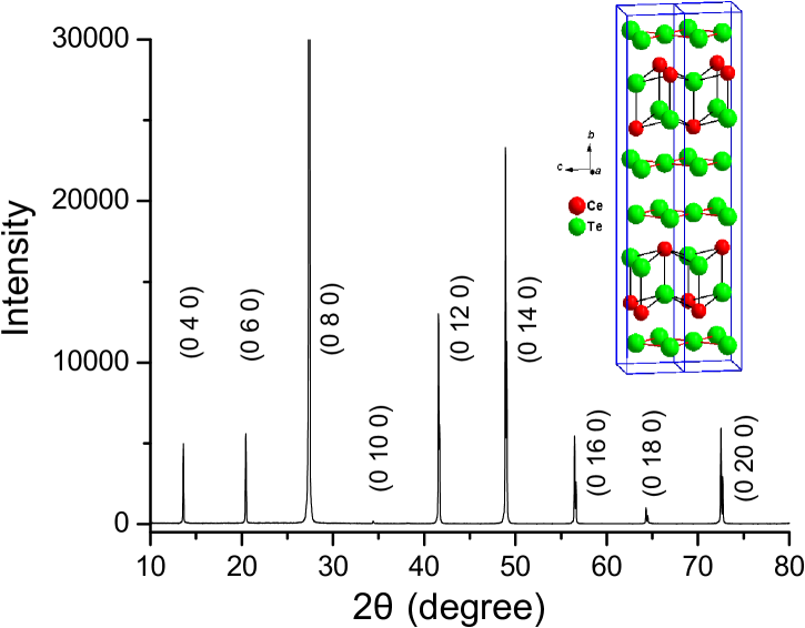
The single crystals of CeTe3 were grown by a self-flux methodmaterial . Ce and Te elements with the molar ratio of 1:40 were mixed, then put into a alumina crucible and sealed in a quartz tube under vacuum. The mixture was heated to 860 0C and stayed for 10 hours, then slowly cooled to 560 0C at a rate of 3 0C/h. At the end temperature the rest flux Te is still in liquid and separated from the crystals in a centrifuge. Plate-like single crystals with the dimension of 33 mm2 were obtained after breaking the crucible. The samples are stored in a glove-box under argon atmosphere since the compound is somewhat air and moisture sensitive. The crystals were characterized by the x-ray diffraction (XRD) and scanning electron microscopy (SEM) measurements. Figure 1 shows the (0k0) XRD patterns for the single crystal samples of CeTe3 with Cu K radiation. The XRD patterns indicate that the samples are of the characteristic of good crystallization along the b axis. The obtained b-axis lattice parameter is b=26.0348 , which is consistent with reported lattice parameter in literaturequenchCDW . The energy dispersive spectroscopy (EDS) analysis equipped with the SEM indicates the correct Ce:Te=1:3 ratio.
The temperature dependent in-plane (ac-plane) resistivity was obtained by the four contact technique in a Quantum Design physical properties measurement system (PPMS) and plotted in figure 2. The resistivity shows good metallic behavior below room temperature. In agreement with previous studiesmaterial , a sharp drop near 3 K is observed, which could be attributed to the antiferromagnetic ordering of the spins from the localized 4f electrons of Cematerial ; CeTe3mulphase ; magRTe3 . The above characterizations indicate a good quality of the single crystal.

The near-normal incident reflectance spectra were measured by Bruker IFS 113v and 66v/s spectrometers in the frequency range from 40 to 25000 cm-1. An in situ gold and aluminium overcoating technique was used to get the reflectivity R(). The real part of conductivity is obtained by the Kramers-Kronig transformation of R(). A Hagen-Rubens relation was used for low frequency extrapolation. A constant value was used for high frequency extrapolation up to 100000 cm-1, above which a dependence is employed.
Figure 3 shows the R() spectra up to 6500 cm-1 with its inset revealing the expanded range up to 25000 cm-1 . Meanwhile, the real part of conductivity is displayed in figure 4. At room temperature, the reflectance R() shows rather high values at low frequency, but decreases rapidly with increasing frequency. A pronounced dip is seen near 3500 cm-1 . This leads to a strong peak in the , roughly near 4600 cm-1 . The spectra provides optical evidence for the presence of an energy gap at room temperature2CDW . The room temperature data are consistent with those reported in earlier studiesRTe3che.pres . Besides this peak in the mid-infrared region, there exists a very sharp Drude component centered at zero frequency. The spectra demonstrate that the compound remains metallic even it is in the CDW state. This is also clearly illustrated in the above resistivity measurementmaterial . Obviously, the Fermi surfaces are only partially gapped in the CDW stateARPESCeTe3400meV ; ARPESCeTe3 ; ARPESRTe3 .
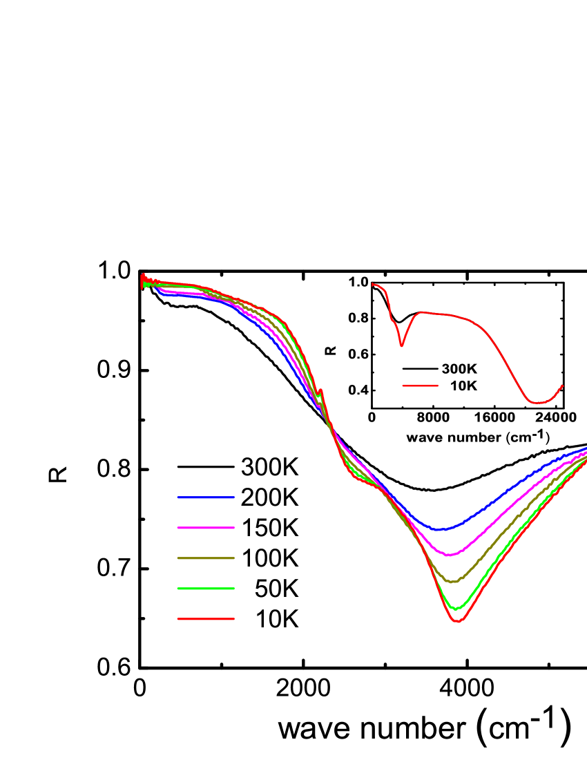
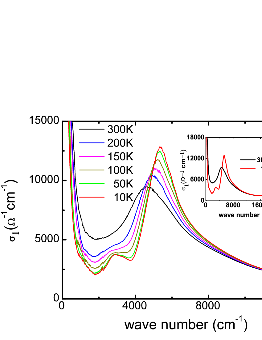
Surprising results were observed at low temperatures. Roughly above but near 200 K, we can identify the development of a new shoulder near 2700 cm-1 in R() and it becomes more and more dramatic with the temperature decreasing. Furthermore, the dip near 3500 cm-1 shifts to higher frequency and becomes much more pronounced than the high temperature data. Then, in the spectra, a new peak develops near 2800 cm-1 . Meanwhile, the spectral weight in the mid-infrared region near this area is strongly suppressed and transferred to the very strong peak near 5000 cm-1 , causing a sizeable shift of original CDW gap towards higher energy. The transfer of the spectral weight is clearly seen in the inset of Fig. 4. As we shall explain below, the new peak developed near 200 K is an indication of new energy gap structure, which could be ascribed to the formation of a new CDW order. The change of the spectral weight at higher energies suggests that the band structure is substantially reconstructed with the formation of the new orderARPESCeTe3400meV . Additionally, the free carrier behaviors also change in response to the formation of the new CDW gap. The reflectance edge near 2500 cm-1 becomes sharper than the edge at high temperatures, reflecting a reduction of the free carrier scattering rate.
It is also worth noting that a small peak feature near 2200 cm-1 in R() develops along with the appearance of the above mentioned shoulder while temperature decreases, which also leads to a peak in the spectra roughly at the same frequency. Different from the notable shift of the two broad peaks corresponding with the two CDW orders, the small peak position changes little at varied temperatures. We noticed that it couldn’t be ascribed to the phonon mode because it locates at such high energy which is not expected based on the atomic mass of both Ce and Te. The origin of the peak remains to be explored.
III DISCUSSION
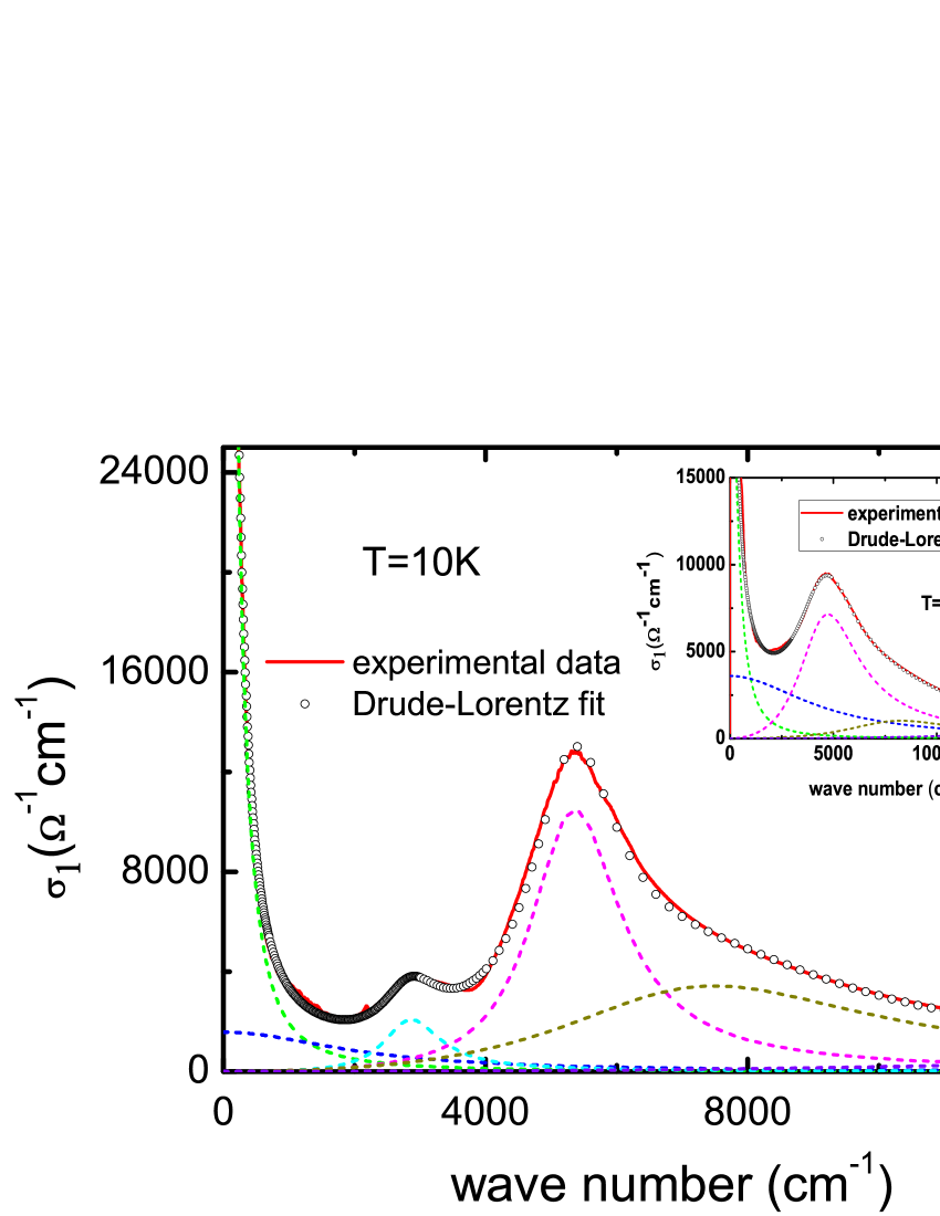
We shall first elaborate the change of the conducting electrons with the development of the new energy gap. To estimate in a quantitative way, we decompose the conductivity spectra into Drude and Lorentz components at two representative temperatures, 300 K, the room temperature, and 10 K, the lowest measurement temperature:
| (1) |
Here, is the dielectric constant at high energy, the middle and last terms are the Drude and Lorentz components, respectively. The results are shown in Fig. 5. At room temperature, the spectrum could be well reproduced by two Drude components and two Lorentz terms. The two Drude components, one with very narrow peak width and one with much broader peak width, describe the conducting carrier responses arising from different bands or Fermi surfaces. The Lorentz peak structure near 4800 cm-1 reflects the CDW gap. At 10 K, one more Lorentz component near 2800 cm-1 is added to reproduce the new CDW gap feature. However, the broader Drude component becomes intensively suppressed while the narrow Drude component displays a relatively smaller change. The fit parameters for the Drude-Lorentz model are listed in table 1. In general, we found that both the and 1/ decrease at lower temperature. This result could be easily interpreted: the formation of the new CDW gap further removes those electrons near EF which experience stronger scattering, leading to a reduction of conducting carrier density; meanwhile the scattering rate is reduced due to the reduction of scattering channels. It is noted that in the dc resistivity (T) of CeTe3, no obvious anomaly below 300 K was observed2CDW . This is also understandable. From the semi-classic Boltzmann transport theory, the resistivity is determined by the complex function of Fermi velocity, the scattering rate, and their weighted integral over the whole FS. Whether (T) shows an anomaly depends on the balance of those quantities which could experience substantial changes across the transition.
The central issue of the present paper is the observation of the new gap feature at about 2800 cm-1 near 200 K. As the gap formation is a characteristic feature for a density wave instability, the structure could naturally be ascribed to a new CDW order at low temperature. From the analysis of the free carrier response, we found that the new CDW order mainly occurs in the bands or Fermi surfaces responsible for the broader Drude component. Those states were gapped away from the Fermi level EF. As we already pointed out, not only those states were affected by the new order, the bands far away from the EF were also influenced as well, because the gap corresponding to the first CDW at high temperature was shifted to higher energy, and there is a spectral weight transfer from the low energy to high energy as well.
300K 27 0.42 31 4.5 – – – 4.7 3.5 39 8.3 6.6 20 10K 27 0.17 14 2.1 2.9 1.1 11 5.4 1.6 32 7.5 5.9 35
It deserves to remark that the new CDW order developed at low temperature in CeTe3 as indicated by the present measurement was not seen by any other experimental techniques previouslyARPESCeTe3400meV ; ARPESCeTe3 ; RTe3che.pres ; CeTe3pres ; magRTe3 ; CeTe3mulphase ; 2CDW . We emphasize here that the optical spectroscopy measurement is a bulk probe technique. One needs to further examine carefully the data from other measurement techniques. In fact, the two different CDW orders were observed in a number of heavy rare-earth based RTe3 compounds with the second transitions occurring between 50 to 200 K2CDW ; ARPES2CDW ; opticsHoEr , our measurement suggests that similar second CDW transition is also present in the light rare-earth element based compound. Even if the static CDW is not formed, the very strong CDW fluctuations are already present.
IV CONCLUSIONS
To conclude, we report an optical study of the single crystal CeTe3, a rare-earth element tri-telluride, which belongs to the layered quasi-two-dimensional charge density wave systems. We observed strongly temperature dependent optical spectra, which is in sharp contrast to the early report. Besides the large CDW gap feature which already exists at room temperature, we also observed the development of another CDW order near 200 K. The second CDW gap at low temperature removes the electrons near EF which undergo large scattering. The Fermi surface is still partially gapped with good metallic behavior exhibiting in the entire temperature range.
ACKNOWLEDGMENTS
This work is supported by the National Science Foundation of China, the Chinese Academy of Sciences, and the 973 project of the Ministry of Science and Technology of China.
References
- (1) E. DiMasi, M. C. Aronson, J. F. Mansfield, B. Foran, and S. Lee, Phys. Rev. B 52, 14516 (1995).
- (2) A. Sacchetti, L. Degiorgi, T. Giamarchi, N. Ru, and I. R. Fisher, Phys. Rev. B 74, 125115 (2006).
- (3) N. Ru, C. L. Condron, G. Y. Margulis, K. Y. Shin, J. Laverock, S. B. Dugdale, M. F. Toney, and I. R. Fisher, Phys. Rev. B 77, 035114 (2008).
- (4) V. Brouet, W. L. Yang, X. J. Zhou, Z. Hussain, R. G. Moore, R. He, D. H. Lu, Z. X. Shen, J. Laverock, S. B. Dugdale, N. Ru, and I. R. Fisher, Phys. Rev. B 77, 235104 (2008).
- (5) A. Sacchetti, C. L. Condron, S. N. Gvasaliya, F. Pfuner, M. Lavagnini, M. Baldini, M. F. Toney, M. Merlini, M. Hanfland, J. Mesot, J. H. Chu, I. R. Fisher, P. Postorino, and L. Degiorgi, Phys. Rev. B 79, 201101(R) (2009).
- (6) A. Sacchetti, E. Arcangeletti, A. Perucchi, L. Baldassarre, P. Postorino, S. Lupi, N. Ru, I. R. Fisher, and L. Degiorgi, Phys. Rev. Lett. 98, 026401 (2007).
- (7) M. Lavagnini, A. Sacchetti, C. Marini, M. Valentini, R. Sopracase, A. Perucchi, P. Postorino, S. Lupi, J. H. Chu, I. R. Fisher, and L. Degiorgi, Phys. Rev. B 79, 075117 (2009).
- (8) D. A. Zocco, J. J. Hamlin, T. A. Sayles, M. B. Maple, J. H. Chu and I. R. Fisher, Phys. Rev. B 79, 134428 (2009).
- (9) B. K. Norling and H. Steinfink, Inorg. Chem. 5, 1488 (1966).
- (10) E. DiMasi, B. Foran, M. C. Aronson, and S. Lee, Chem. Mater. 6, 1867 (1994).
- (11) V. Brouet, W. L. Yang, X. J. Zhou, Z. Hussain, N. Ru, K.Y. Shin, I. R. Fisher, and Z. X. Shen, Phys. Rev. Lett. 93, 126405 (2004).
- (12) N. Ru and I. R. Fisher, Phys. Rev. B 73, 033101 (2006).
- (13) J. Laverock, S. B. Dugdale, Zs. Major, M. A. Alam, N. Ru, I. R. Fisher, G. Santi, and E. Bruno, Phys. Rev. B 71, 085114 (2005).
- (14) H. Komoda, T. Sato, S. Souma, T. Takahashi, Y. Ito, and K. Suzuki, Phys. Rev. B 70, 195101 (2004).
- (15) G. H. Gweon, J. D. Denlinger, J. A. Clack, J. W. Allen, C. G. Olson, E. D. DiMasi, M. C. Aronson, B. Foran, and S. Lee, Phys. Rev. Lett. 81, 886 (1998).
- (16) N. Ru, J. H. Chu, and I. R. Fisher, Phys. Rev. B 78, 012410 (2008).
- (17) R. G. Moore, V. Brouet, R. He, D. H. Lu, N. Ru, J. H. Chu, I. R. Fisher, and Z. X. Shen, Phys. Rev. B 81, 073102 (2010).
- (18) F. Pfuner, P. Lerch, J. H. Chu, H. H. Kuo, I. R. Fisher, and L. Degiorgi, Phys. Rev. B 81, 195110 (2010).