Coexistence of the topological state and a two-dimensional electron gas on the surface of Bi2Se3
Topological insulators are a recently discovered class of materials with fascinating properties: While the inside of the solid is insulating, fundamental symmetry considerations require the surfaces to be metallic Fu:2007b ; Fu:2007c ; Moore:2007 ; Hsieh:2008 ; Zhang:2008 ; Moore:2010 . The metallic surface states show an unconventional spin texture Hsieh:2009 ; Hsieh:2009b , electron dynamics Pascual:2004 ; Konig:2007 ; Roushan:2009 ; Alpichshev:2010 and stability. Recently, surfaces with only a single Dirac cone dispersion have received particular attention Hsieh:2009b ; Hsieh:2009c ; Xia:2009 ; Zhang:2009 ; Chen:2009 ; Lin:2010a ; Lin:2010b . These are predicted to play host to a number of novel physical phenomena such as Majorana fermions Fu:2008 , magnetic monopoles Qi:2009b and unconventional superconductivity Lindner:2010 . Such effects will mostly occur when the topological surface state lies in close proximity to a magnetic or electric field, a (superconducting) metal, or if the material is in a confined geometry. Here we show that a band bending near to the surface of the topological insulator Bi2Se3 gives rise to the formation of a two-dimensional electron gas (2DEG). The 2DEG, renowned from semiconductor surfaces and interfaces where it forms the basis of the integer and fractional quantum Hall effects Klitzing:1980 ; Tsui:1982 , two-dimensional superconductivity Reyren:2007 , and a plethora of practical applications Ando:1982 , coexists with the topological surface state in Bi2Se3. This leads to the unique situation where a topological and a non-topological, easily tunable and potentially superconducting, metallic state are confined to the same region of space.
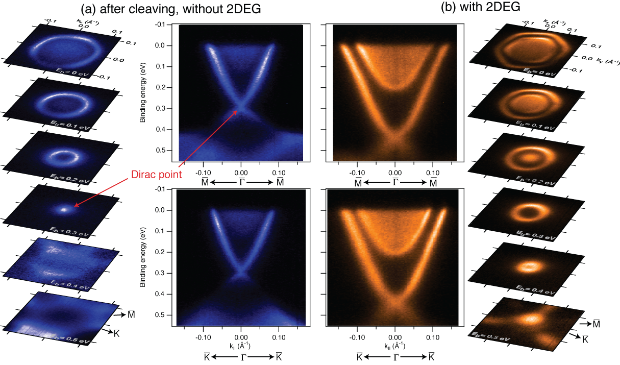
The emergence of a 2DEG on the (0001) surface of Bi2Se3 can be followed by angle-resolved photoemission (ARPES), as shown in Fig. 1. Immediately after cleaving the sample, a sharp V-shaped topological state is observed in the gap. Features stemming from the bulk valence and conduction bands are also seen. The latter should not be observable by photoemission for an intrinsic semiconductor, but most as-grown Bi2Se3 crystals turn out to be degenerately electron-doped Urazhdin:2004 ; Hsieh:2009c . Over a period of a few hours (depending on the sample temperature), spectral changes are observed: The chemical potential shifts gradually upwards, an effect which has been ascribed to a defect-induced downward band bending near the surface Hsieh:2009c . Eventually, we find that an intense and narrow rim emerges around the bottom of the conduction band (Fig. 1(b)). This state is assigned to a quantum-confined 2DEG, similar to what has been found for other narrow-gap semiconductors Piper:2008 ; King:2010 . After about three hours the situation becomes more stable, with the sample gradually deteriorating but no further pronounced shifts of the chemical potential.
Fig. 1(b) also shows the dispersion of the topological state and the two-dimensional electron gas as constant energy cuts through a three-dimensional data set. The topological state has a circular constant energy contour near the Dirac point, but all the states (topological state, 2DEG and conduction band) show hexagonal contours near the Fermi level (435 meV above the Dirac point). This hexagonal warping of the topological state is apparent from its different Fermi wavevectors of and 0.128(1) Å-1 along the and directions, respectively. Similar deviations from an ideal Dirac cone shape have already been described for the case of Bi2Te3 Chen:2009 ; Fu:2009 where the effect is more pronounced than here. For the conduction band and the 2DEG, the hexagonal shape implies a non-isotropic effective mass, a point we shall return to later.
It is important to note the very different physical nature of the topological state and the 2DEG. The former is completely non spin-degenerate, apart from the Dirac point. As such, its quasiparticles are protected from back-scattering. The band structure does not permit the opening of energy gaps due to a small perturbation, or the formation of metal-insulator transitions in the form of charge density waves, despite the strongly nested Fermi surface Kim:2005b (a spin-density wave would be permitted Fu:2009 ). The 2DEG, on the other hand, is spin degenerate and could be prone to such instabilities. In fact, a hexagonal Fermi surface with its strong nesting has, to the best of our knowledge, not yet been observed for such a state.
Most importantly, the existence of the 2DEG opens new decay channels for the topological state. An indication of this is the change in the linewidth of the latter. Immediately after cleaving the crystal, the topological state is found to be very narrow, of the order of Å-1 at the Fermi level. If we interpret this width as a measure for the inverse mean free path on the surface , this would correspond to ÅKevan:1986 . This value is similar to what is found for highly perfect epitaxial graphene Bostwick:2007 or cleaved high-temperature superconductors Borisenko:2006a . A long mean free path for the topological state is, of course, expected from the reduced phase space for scattering Nechaev:2009 . Once the 2DEG is established at the surface, the width of the topological state is increased to Å-1, while the 2DEG state is slightly wider ( Å-1). Apart from the presumably small increased number of defects near the surface, the increased width of the topological state is almost certainly related to the presence of the 2DEG itself, and the scattering processes now permitted between this and the topological state.
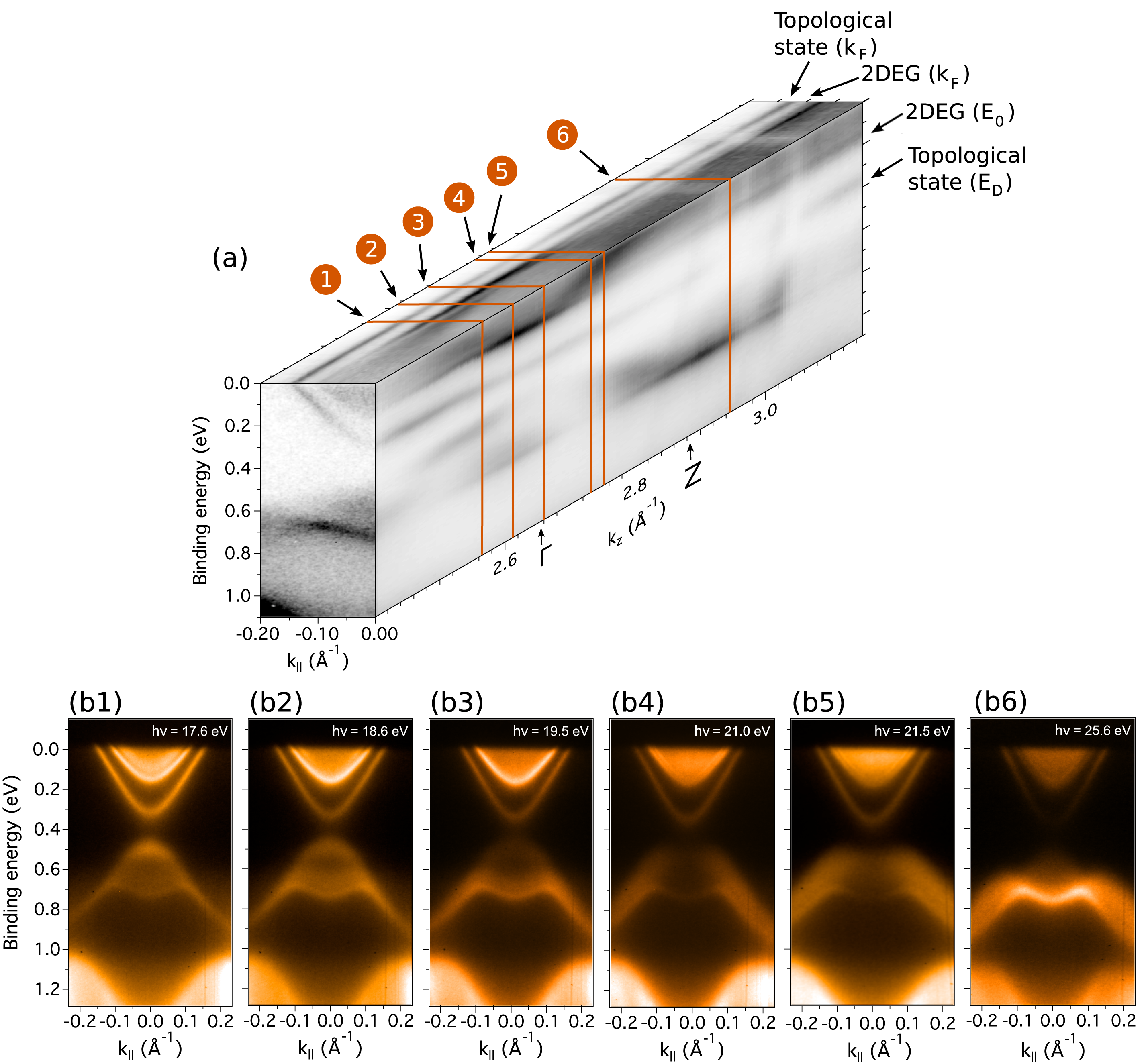
The dimensionality of all of the observed states can be probed directly by performing ARPES measurements at different photon energies, thus varying the wave vector perpendicular to the surface, . Fig. 2(a) shows the result of such measurements, revealing the evolution of the electronic states on the Fermi surface, and within 1.1 eV of the Fermi level at , with . Selected measurements at different photon energies are also shown in Fig. 2(b) (the full data set is available in the supplementary material). Both the topological state and the 2DEG do not disperse with , confirming their two-dimensional nature: they occur at the same energy and momentum in Figs. 2(b1–6) and give rise to linear features on both the and the planes (Fig. 2(a)). In contrast, a strong -dispersion of the bulk conduction (valence) band is evident, showing a maximum (minimum) in binding energy at the bulk point at Å-1. This dispersion also explains the photon-energy-dependent “filling” of the 2DEG contour, due to emission from bulk conduction band states (Fig. 2(b1) and (b3)).
While the topological and 2DEG states do not disperse in , these spectral features do show strong intensity variations with photon energy. Such a -dependence of the photoemission intensity of two-dimensional states is well known for metallic surface states, due to transition matrix element effects Louie:1980 ; Hofmann:2002 . From Fig. 2(a), emission from the 2DEG is resonantly enhanced when the conduction band reaches its minimum at the bulk point. In the plane (Fig. 2(a)), another state is observed at a binding energy of 750 meV which does not disperse with . This corresponds to the M-shaped feature in the individual cuts, particularly pronounced in Fig. 2(b6). We interpret this as another surface state, situated in a projected bulk band gap below the upper valence band near Xia:2009 . Similar to the 2DEG, emission from this state is resonantly enhanced when the bulk valence band dispersion reaches a minimum at the Z point ( 2.9 Å-1).
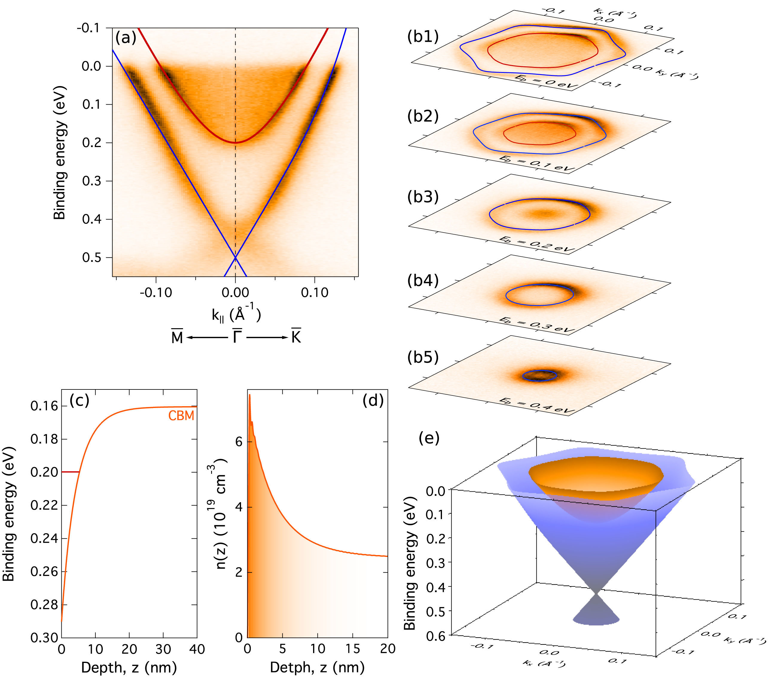
The 2DEG on the surface is derived from the conduction band states, as indicated by its resonant enhancement near , but confined in the -direction due to a strong band bending near the surface. We have performed model calculations to further substantiate the existence and origins of this 2DEG, as shown in Fig. 3. The near-surface band bending of the material and the dispersions of the resulting 2DEG states are calculated via a coupled solution of the Poisson and Schrödinger equations, based around the method described in Ref. King:2008 . These calculations accurately reproduce the measured dispersion and constant energy contours of the 2DEG state, shown in Fig. 3(a,b), for a downward band bending at the surface of 0.13 eV (Fig. 3(c)), very similar to the shift of the Dirac point between the freshly cleaved sample and following development of the 2DEG. It is this band bending which creates a potential well at the surface, causing quantum-confinement of the conduction band states, and development of the 2DEG. In the presence of a potential gradient, one may expect to observe a Rashba spin-splitting of the 2DEG state. However, from a simple model using the calculated band bending potential gradient, we estimate an upper limit for the Rashba splitting of only Å-1 at the Fermi level, unlikely to be observable in practice.
In addition to the main 2DEG state located meV below the conduction band edge of the bulk (shown in Fig. 3(c), and clearly apparent in the measured data (Fig. 3(a)), a second 2DEG state is predicted in the calculations at only meV below the bulk band edge. This state is not shown in Fig. 3 because, being so shallow, its wavefunctions will be very extended in : consequently, we would expect this state to be very delocalized and to largely contribute to the diffuse intensity above the lower 2DEG state. However, we note that at some photon energies, a second state is discernible above the 2DEG band bottom (for example, Figs. 2(b4,5)). This second state is situated approximately 35 meV above the band bottom of the main 2DEG state, and so would be consistent with a second very shallow state as predicted by the calculations.
The hexagonal Fermi surface contour of the 2DEG state implies an anisotropic in-plane effective mass, and we find values of 0.122m0 and 0.109m0 along and , respectively. The 2DEG state also exhibits some deviations from parabolicity. We attribute this to a interaction Kane:1957 between the conduction and valence bands, which we include within our calculations. A model has also been proposed to describe the hexagonal warping of the topological surface state in Bi2Te3 Fu:2009 . This model reproduces the dispersions and constant energy contours of the topological state observed here reasonably well (Fig. 3(a,b)), although the magnitude of the hexagonal warping term is approximately a factor of 2.3 smaller than that estimated from the measured Fermi velocity and wavevector, using the formalism within Ref. Fu:2009 .
The model calculations confirm the experimental findings presented above that a downward band bending at the surface of Bi2Se3 induces a two-dimensional electron gas, that co-exists with the topological surface state (Fig. 3(e)). This suggests the potential to modulate the 2DEG density via control of the band bending, either through absorption of elemental or molecular species on the clean surface, or via a gate electrode. Such a scheme could potentially be used to obtain a switchable metallic, and possibly superconducting, layer in the vicinity of the topological surface state, which could be fundamental to the incorporation of the novel properties of topological insulators into device applications.
Methods Summary Single crystals of Bi2Se3 were grown as follows: Stoichiometric mixtures of 5N purity elemental Bi and Se were melted at 860 ∘C for 24 hours in an evacuated quartz ampoule, cooled down to 650 ∘C at a rate of 2.5 ∘C/h, and then annealed at 650 ∘C for another two days. The sample was then removed to another evacuated quartz ampoule with a conical bottom and zone melted through an induction coil with a rate of 1.2 mm/h.
Angle-resolved photoemission measurements were performed at the SGM-3 beamline of the ASTRID synchrotron radiation facility in Aarhus. The samples were cleaved at room temperature and ARPES data were taken at around 60 K. Between cleaving and the reported measurements, the sample temperature was thus above 60 K, such that the more rapid change in the Fermi energy compared to that reported by Hsieh et al. Hsieh:2009c can be explained by the higher sample temperature. For the detailed mapping of the states, the energy and angular resolutions were set to better than 10 meV and 0.13∘, respectively. The photon energy for the data in Figs. 1 and 3 was 16 eV. For the photon energy scan in Fig. 2, the energy resolution was better than 20 meV. The values for the three-dimensional representation of the photon energy scan of Fig. 2 were calculated using free-electron final states, i.e. , where is the emission angle and is the inner potential, chosen to be 11.8 eV, in good agreement with Ref. Xia:2009 . The intensity of each individual image has been normalized such that the maximum amount of detail is visible in the maps.
The coupled Poisson-Schrödinger calculations King:2008 were performed incorporating both the non-parabolicity of the conduction band dispersion as well as the anisotropy of the effective mass along different crystallographic directions. The in-plane mass was taken as 0.122m0 and 0.109m0 along the and directions, respectively, where m0 is the free-electron mass. Along kz, an effective mass of 0.24m0 was used, estimated from the bulk conduction band dispersion shown in Fig. 2(a). The band gap was taken as 350 meV, and a bulk dielectric constant of 113 was used. The bulk carrier density was set at cm-3, corresponding to a bulk Fermi level 0.16 eV above the conduction band edge, as estimated from the ARPES data.
Acknowledgements Financial support from the Danish Council for Independent Research and the Danish National Research Foundation is gratefully acknowledged.
References
- (1) Fu, L. & Kane, C. L. Topological insulators with inversion symmetry. Physical Review B 76, 045302 (2007).
- (2) Fu, L., Kane, C. L. & Mele, E. J. Topological insulators in three dimensions. Physical Review Letters 98, 106803 (2007).
- (3) Moore, J. E. & Balents, L. Topological invariants of time-reversal-invariant band structures. Phys. Rev. B 75, 121306 (2007).
- (4) Hsieh, D. et al. A topological dirac insulator in a quantum spin Hall phase. Nature 452, 970–974 (2008).
- (5) Zhang, S. C. Topological states of quantum matter. Physics 1, 6 (2008).
- (6) Moore, J. E. The birth of topological insulators. Nature 464, 194–198 (2010).
- (7) Hsieh, D. et al. Observation of unconventional quantum spin textures in topological insulators. Science 323, 919–922 (2009).
- (8) Hsieh, D. et al. Observation of time-reversal-protected single-dirac-cone topological-insulator states in Bi2Te3 and Sb2Te3. Physical Review Letters 103, 146401 (2009).
- (9) Pascual, J. I. et al. Role of spin in quasiparticle interference. Physical Review Letters 93, 196802 (2004).
- (10) Konig, M. et al. Quantum spin hall insulator state in HgTe quantum wells. Science 318, 766–770 (2007).
- (11) Roushan, P. et al. Topological surface states protected from backscattering by chiral spin texture. Nature 460, 1106–1109 (2009).
- (12) Alpichshev, Z. et al. Stm imaging of electronic waves on the surface of Bi2Te3: Topologically protected surface states and hexagonal warping effects. Phys. Rev. Lett. 104, 016401 (2010).
- (13) Hsieh, D. et al. A tunable topological insulator in the spin helical Dirac transport regime. Nature 460, 1101–1105 (2009).
- (14) Xia, Y. et al. Observation of a large-gap topological-insulator class with a single dirac cone on the surface. Nat Phys 5, 398–402 (2009).
- (15) Zhang, H. et al. Topological insulators in Bi2Se3, Bi2Te3 and Sb2Te3 with a single Dirac cone on the surface. Nat Phys 5, 438–442 (2009).
- (16) Chen, Y. L. et al. Experimental realization of a three-dimensional topological insulator, Bi2Te3. Science 325, 178–181 (2009).
- (17) Lin, H. et al. Half-heusler ternary compounds as new multifunctional experimental platforms for topological quantum phenomena. Nat Mater 9, 546–549 (2010).
- (18) Lin, H. et al. Single-dirac-cone topological surface states in the TlBiSe2 class of topological semiconductors. Phys. Rev. Lett. 105, 036404 (2010).
- (19) Fu, L. & Kane, C. L. Superconducting proximity effect and Majorana fermions at the surface of a topological insulator. Phys. Rev. Lett. 100, 096407 (2008).
- (20) Qi, X.-L., Li, R., Zang, J. & Zhang, S.-C. Inducing a magnetic monopole with topological surface states. Science 323, 1184–1187 (2009).
- (21) Linder, J., Tanaka, Y., Yokoyama, T., Sudbø, A. & Nagaosa, N. Unconventional superconductivity on a topological insulator. Phys. Rev. Lett. 104, 067001 (2010).
- (22) Klitzing, K. v., Dorda, G. & Pepper, M. New method for high-accuracy determination of the fine-structure constant based on quantized hall resistance. Phys. Rev. Lett. 45, 494–497 (1980).
- (23) Tsui, D. C., Stormer, H. L. & Gossard, A. C. Two-dimensional magnetotransport in the extreme quantum limit. Phys. Rev. Lett. 48, 1559–1562 (1982).
- (24) Reyren, N. et al. Superconducting interfaces between insulating oxides. Science 317, 1196–1199 (2007).
- (25) Ando, T., Fowler, A. B. & Stern, F. Electronic properties of two-dimensional systems. Rev. Mod. Phys. 54, 437–672 (1982).
- (26) Urazhdin, S. et al. Surface effects in layered semiconductors Bi2Se3 and Bi2Te3. Phys. Rev. B 69, 085313 (2004).
- (27) Piper, L. F. J. et al. Observation of quantized subband states and evidence for surface electron accumulation in cdo from angle-resolved photoemission spectroscopy. Physical Review B 78, 165127 (2008).
- (28) King, P. D. C. et al. Surface band-gap narrowing in quantized electron accumulation layers. Phys. Rev. Lett. 104, 256803 (2010).
- (29) Fu, L. Hexagonal warping effects in the surface states of the topological insulator Bi2Te3. Phys. Rev. Lett. 103, 266801 (2009).
- (30) Kim, T. K. et al. Evidence against a charge density wave on Bi(111). Physical Review B 72, 085440 (2005).
- (31) Kevan, S. Direct measure of surface impurity scattering by angle-resolved photoemission. Physical Review B 33, 4364 (1986).
- (32) Bostwick, A., Ohta, T., Seyller, T., Horn, K. & Rotenberg, E. Quasiparticle dynamics in graphene. Nature Physics 3, 36–40 (2007).
- (33) Borisenko, S. V. et al. Kinks, nodal bilayer splitting, and interband scattering in YBa2Cu3O6+x. Physical Review Letters 96, 117004 (2006).
- (34) Nechaev, I. A. et al. Hole dynamics in a two-dimensional spin-orbit coupled electron system: Theoretical and experimental study of the Au(111) surface state. Physical Review B 80, 113402 (2009).
- (35) Louie, S. G. et al. Periodic oscillations of the frequency-dependent photoelectric cross sections of surface states: Theory and experiment. Physical Review Letters 44, 549–553 (1980).
- (36) Hofmann, P. et al. Unexpected surface sensitivity at high energies in angle-resolved photoemission. Physical Review B 66, 245422 (2002).
- (37) King, P. D. C., Veal, T. D. & McConville, C. F. Nonparabolic coupled poisson-schr[o-umlaut]dinger solutions for quantized electron accumulation layers: Band bending, charge profile, and subbands at inn surfaces. Physical Review B 77, 125305 (2008).
- (38) Kane, E. O. Band Structure of Indium Antimonide. J. Phys. Chem. Solids. 1, 249 (1957).