SWNT-array resonant gate MOS transistor
Abstract
We show that thin horizontal arrays of single wall carbon nanotubes (SWNTs) suspended above the channel of silicon MOSFETs can be used as vibrating gate electrodes. This new class of nano-electromechanical system (NEMS) combines the unique mechanical and electronic properties of SWNTs with an integrated silicon-based motion detection. Its electrical response exhibits a clear signature of the mechanical resonance of SWNTs arrays (120-150 MHz) showing that these thin horizontal arrays behave as a cohesive, rigid and elastic body membrane with a Young modulus in the order of 1-10 GPa and ultra-low mass. The resonant frequency can be tuned by the gate voltage and its dependence is well understood within the continuum mechanics framework.
pacs:
62.25.-g 68.35.Gy 81.07.-b 81.07.Oj 81.16.Dn 85.35.Kt 85.85.+jIt is largely admitted that the future integration of nano-objects within technologically relevant devices and circuits will require their co-integration with the existing CMOS technology. Yet, examples of functional devices and circuits combining the two types of building blocks are extremely scarce. Among the different nano-objects, carbon nanotubes (CNTs) have attracted much attention due to their unique electronic properties. Examples of integration of CNTs with CMOS-based electronic circuits are limited to field effect transistors (FET) [1] and interconnects [2]. Moreover, since CNTs are light and have very large Young’s modulus [3] they constitute an ideal building block for devices such as micro and nano-electromechanical systems (MEMS/NEMS). Most of the efforts to date have primarily focused on individual CNT based nanodevices. For example, a suspended nanotube has been used as a device element of a tuneable electromechanical oscillator [4, 5], sensors [6, 7], rotational actuators [8]. Similarly, a carbon nanotube cantilever has been used in scanning probe microscope tips [9], nanotweezers [10], switches [11, 12] and relays [13] and even a nanotube radio [14]. These demonstrations mainly require dedicated nanofabrication steps for aligning the measuring circuit to the position of individual CNTs and/or tedious and time consuming manipulation of CNTs, making the realization of reliable and integrated nanodevices impractical. Recently an elegant approach was demonstrated to circumvent this problem, by synthesizing three-dimensional CNT medium composed mostly of highly-oriented and closely packed CNTs [15]. Using this approach, thick “CNT wafers” can be deposited on top of a prefabricated silicon wafer and post-processed, paving the way to the integration of hybrid CNT-silicon devices. In order to assess the potential of “CNT wafers” as micromechanical material, Hayamizu et al. [16] investigated the mechanical properties of thick beams and found that they act as a single cohesive unit described by classical theory of elasticity. On the opposite limit, thin SWNTs arrays used in SWNT-based field effect transistors showed very promising high frequency electronic properties [17]. If in addition these extremely thin SWNT layers show interestring mechanical properties they could serve as a basic material for innovative MEMS/NEMS devices. Of particular interest are movable gate [18, 19] and body FET transistor structures [20, 21] operating as active MEM/NEM resonators, similarly to the very first proposed resonant-Gate transistor [22].
Here we present an alternative way, versatile and well adapted to integrate extremely thin SWNTs arrays to CMOS transistors and demonstrate the first resonant SWNTs array suspended gate FET, fully compatible with any bulk silicon CMOS technology. The SWNTs suspended gate FET device (SWNTs SG-SiFET) combines the virtues of SWNT suspended arrays (stiff and light material used as vibrating gate of a silicon field effect transistor (SiFET)), with the integrated transistor detection. The high frequency vibration of the SWNTs array modulates the charge density in the FET channel and the output signal of the resonator is the drain current. The electrical response shows the signature of the mechanical resonance of SWNTs arrays (120-150 MHz) demonstrating that these extremely thin horizontal arrays behave as a cohesive, rigid and elastic body membrane. The resonant frequency can be tuned by the gate voltage and its dependence is well understood within the continuum mechanics framework.
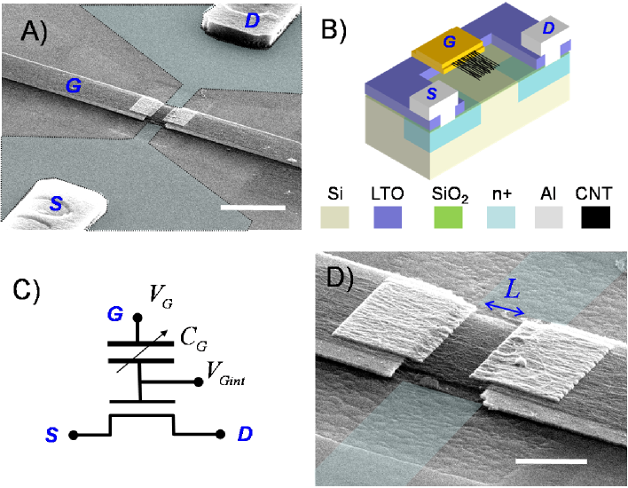
Figure1 shows a micrograph of a SWNTs SG-SiFET and its schematic cross section. The fabrication details of the SiFET are described elsewhere [23]. Suspended SWNTs gates centered on the FET channel were fabricated as follows: First, chromium/platinum Cr/Pt (5 nm/ 60 nm) lines were patterned perpendicular to the FET channel (See 1 A and B). These electrodes were used to deposit a dense array of SWNTs, mostly centered on top of the SiFET channel, by a dielectrophoresis (DEP) process. The DEP step is described in detail elsewhere [17]. The SWNTs used were synthesized by laser ablation, first purified and then dispersed at low concentration in N-methylpyrrolidone using moderate sonication, resulting in a highly stable dispersion comprising mostly individual nanotubes. To give a precise geometry to the SWNTs gate, an e-beam lithography step followed by reactive ion etching (/S) was realized. Finally Ti/Au (10 nm / 50 nm) electrodes were patterned by e-beam lithography and lift-off technique to doubly clamp and electrically contact the SWNTs gate to metallic lines. The SWNTs gate was suspended by etching the sacrificial layer in BHF. This step was done only in the central region, through an e-beam patterned PMMA mask, to avoid damaging of Al electrodes of the SiFET. The e-beam mask was stripped in acetone followed by critical point drying. The final air-gap of the fabricated device is 100nm, with a residual oxide thickness of 35 nm.
The SWNTs array gate is actuated by applying a voltage on the suspended SWNTs membrane gate. The electrostatic force on the SWNTs membrane for and can be well approximated by
| (1) |
where is the first derivative of the gate capacitance per unit length with respect to the gap separation and and the mean value of the channel potential [24]. The first term of (1) corresponds to the DC component that elastically deforms the SWNTs membrane and sets its mechanical tension and the second drives its motion at frequency . The SWNTs membrane motion induced by the AC component of modulates the capacitance which in turn modulates the charge in the channel. The conductance channel change can be written as
| (2) |
To detect this conductance change at we use the device as a mixer: we apply an AC voltage between source and drain [25] and an AC gate voltage chopped by a switch operated at audio frequency (typically 133 Hz, see setup depicted in Figure 2 ).
The source-drain current has a component at which is detected by a lock-in amplifier:
| (3) |
The first term contains the mechanical response of the SWNTs array. For small motional amplitudes, the membrane can be treated as a simple harmonic resonator [26] with effective mass , and , , and are the mass density, width, length and thickness of the membrane respectively. The change in capacitance can be well approximated by where is the displacement of the midpoint of the resonator and can be obtained from the effective harmonic oscillator equation (see Equation (6) below):
| (4) |
Where is the response function of a harmonic oscillator with resonant frequency and quality factor , driven at frequency . Then the lock-in current reads:
| (5) |
Where , and the phase difference between the RF signal on the gate and source electrodes is . Using this expression, data can be fitted and the gate voltage dependence of the resonant frequency and the quality factor can be estimated.
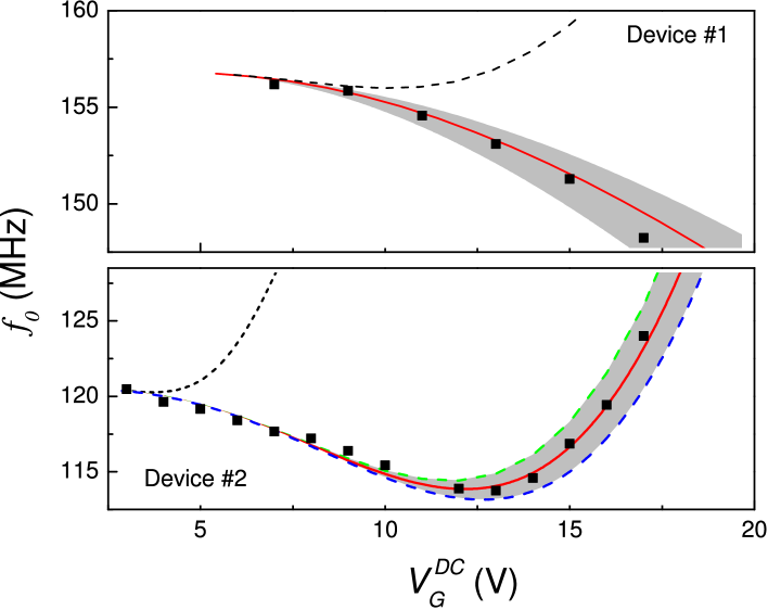
Figure 3 shows the mixing current measured on device #1 ( ) as a function of the excitation frequency for 5 different values of and their best fit using expression (5) and , , , and as fitting parameters. Data were taken in the linear regime (low AC amplitudes) under vacuum ( mbar) and at room temperature. The size of the resonance feature increases with increasing the DC gate voltage making evident the increase of the SWNTs membrane deflection amplitude. The position in frequency of the resonance (in the 150-160 MHz range) moves downward with the increase of the gate voltage showing an counter-intuitive effective softening of the SWNTs membrane spring constant. Thanks to the array configuration, the output signal level of our SWNTs array resonator is approximately one order of magnitude higher than the one reported in Ref.[4] and [28], using a mixing configuration scheme, which highlights the advantages of a hybrid SWNTs/SiFET configuration for building MEM oscillators. Moreover, the output signal level of the SWNTs array SG-SiFET can be further increased by operating the transistor at higher DC (saturation mode). In this work, we mainly focus on the electromechanical behavior of the SWNTs array and in demonstrating the basic operating behavior of such device.
Figure 4 shows the extracted resonant frequency for two different devices: #1 and #2 ( and nm respectively). As expected, the resonant frequency extrapolated to zero gate voltage is higher for device #1 since the array length is smaller. For device #2 we observe a decrease at low gate voltages and a strong increase at higher voltages.
To explain the observed dependence, we consider the SWNTs array as an effective beam [27] and we use a continuum model to describe its electromechanical behavior. Such approach was succefully used in the case of individual MWNTs in Ref.[28]. If we assume that the driving electrostatic force does not change the shape of lowest vibration mode of the SWNTs array , the vertical displacement of the SWNTs array can be approximated by , i.e. a stationary part obeying the beam equation determined by the DC electrostatic force and a small time dependent part obeying the equivalent harmonic oscillator equation (see Supplementary Information (SI) for details)
| (6) |
in (6) the spring constant is determined by the physical and geometrical parameters of the SWNTs array and the mechanical tension set by As can be expected, the spring constant is an increasing function of since the mechanical tension increases with The value of can be obtained by solving self-consistently the beam equation (see SI for details). The second term on the right-hand side of (6) comes from the non-linear dependence of the gate capacitance with the vertical coordinate. This term renormalizes the spring constant and produces a softening of the resonator. Then the resonant frequency of the SWNTs array can be written as follows (see SI for details)
| (7) | |||
where corresponds to the fundamental resonant frequency of a doubly clamped beam, , is the mechanical residual tension when , and . The third and forth terms in (7) are the DC gate voltage dependent hardening of the effective spring constant due to the elastic deformation of the beam. Numerical simulations show that the sum of these two terms can be written as . As a result, the proposed model fits quantitatively our data if .
AFM characterization of our devices shows that the thickness of the SWNTs array is inhomogeneous. The mean value of the SWNTs membrane thickness is about for both devices. The imperfect packing and alignment of SWNTs, that produces the mechanical cohesiveness of the SWNTs membrane, makes its density unknown. However, from data at low gate voltages one could estimate the value of and use its definition to obtain an effective density . This yields: for device #1 and for device #2. Using this estimation and and as fitting parameters one could obtain the results depicted in Figure 4. For comparison we also show the best result considering (black dash curve) and using only as fitting parameter (120 GPa and 610 GPa for device #1 and #2 respectively). The red curves correspond to the best fit: , for device #1 and , for device #2. Gray region represents the uncertainty on the thickness for device #1 and the sensitivity to the value of for device #2. The quantitative agreement makes evident the finite value of an in-built mechanical tension. This mechanical tension can probably be attributed to the suspension step of SWNTs membranes. The impact of dielectrophoresis field on will be further investigated. The value obtained for the Young’s modulus is better than the one reported for bucky paper [30] 2.3 GPa and comparable to the one reported for highly aligned SWNTs [15] or slightly smaller [16], supporting that our SWNTs arrays of thickness as small as 15nm behaves as highly ordered wafers.
The quality factor obtained from fitting is for both devices. This value is comparable to the one reported by Hayamizu et al. [16] for highly aligned SWNTs thick cantilevers () and suspended graphene [31] but lower than the one reported for single arc discharged SWNTs [9]. One possible explanation is related to the energy loss due to loosely linked SWNTs inside the membrane. This value could be improved by suppressing the sliding among SWNTs via cross-linking between them, as suggested in [32].
In conclusion, SWNT suspended membrane gates were succesfuly integrated to MOS transistors and operated at high frequency for the first time. These extremely thin membranes behave as a cohesive, rigid and elastic body. In particular, the resonant frequency of SWNTs SG-SiFETs is tuned by the DC gate voltage and its dependence can be well described within the continuum mechanics framework. The mechanical properties of SWNTs arrays are comparable to those observed in closely packed and aligned SWNTs wafers [15]. The quality factor observed makes SWNTs membranes more suitable for high frequency mechanical switching devices because of the quick damping of vibration. This work shows promise to realize devices with practical application using CNT, for example in bio-sensing and RF electronics.
References
- [1] Tseng Y 2004 et al. Nano Lett., 4 123
- [2] Close G F 2008 et al. Nano Lett.8 706
- [3] Treacy M M J, Ebbesen T W, Gibson J M 1996 Nature 381 678.
- [4] Sazonova V et al.2004 Nature 431 284
- [5] Witkamp B, Poot M and van der Zant H S J 2006 Nano Lett. 12 2904
- [6] Kong J et al. 2000 Science 287 622
- [7] Stampfer, et al. 2006 Nano Lett. 6 233
- [8] Fennimore A M, et al. 2003 Nature 424 408
- [9] Dai H et al. 1996 Nature 384 147
- [10] Kim P and Lieber C M 1999 Science 286 2148
- [11] Dujardin E, et al. 2005 Appl. Phys. Lett. 87 193107
- [12] Jang J E , et al. 2008 Nat. Nanotechnol. 3 26
- [13] Lee S W et al. 2004 Nano Lett. 4 2027
- [14] Jensen K, Weldon J, Garcia H and Zettl A 2007 Nano Lett. 7 3508
- [15] Hayamizu Y. et al. 2008 Nat. Nanotechnol. 3 289
- [16] Hayamizu Y et al. 2009 Phys. Rev. Lett. 102 175505.
- [17] Le Louarn A et al. 2007 Appl. Phys. Lett. 90 233108
- [18] Abele N, et al. 2005 Technical IEEE International Digest Electron Devices Meeting, IEDM 479 1967
- [19] Durand C et al. 2008 IEEE Electron Device Letters 29 494
- [20] Grogg D, et al. 2008 Digest of Annual Device Research Conference, DRC 2008 155
- [21] Grogg D, et al. 2008 IEEE International Electron Devices Meeting, IEDM 2008 1.
- [22] Nathanson H C, et al. 1967 IEEE Transactions on Electron Devices, ED-14(3) 117
- [23] Arun A et al. 2010 IEEE proceedings of MEMS 2010 112
- [24] SI describes the procedure used to estimate its value.
- [25] The phase difference between the gate and source electrode depends on the frequency of the rf signals, on the (gate dependent) conductance of the nanotube, and on its derivative. Moreover, the lock-in detected phase does not contain any information about .
- [26] Yurke B et al. 1995 Phys. Rev. A 51 4211
- [27] As a first approximation we consider the membrane as a beam neglecting the correction due to the Poisson’s ratio. This is justified by the small value generally observed for the shear modulus in this material.
- [28] Lefevre R, et al. 2005 Phys. Rev. Lett. 95 185504
- [29] Saito R Dresselhaus G and Dresselhaus M S 1998 Physical Properties of Carbon Nanotubes (London: Imperial College Press
- [30] Coleman J N et al. 2003 Appl. Phys. Lett. 82 1682
- [31] Scott Bunch J, et al. 2007 Science 315 490; Chen C, et al. 2009 Nat. Nanotechnol. 4 861
- [32] Kis A, et al. 2004 Nat. Mater. 3 153