Atom chips with two-dimensional electron gases: theory of near surface trapping and
ultracold-atom microscopy of quantum electronic systems
Abstract
We show that current in a two-dimensional electron gas (2DEG) can trap ultracold atoms m away with orders of magnitude less spatial noise than a metal trapping wire. This enables the creation of hybrid systems, which integrate ultracold atoms with quantum electronic devices to give extreme sensitivity and control: for example, activating a single quantized conductance channel in the 2DEG can split a Bose-Einstein condensate (BEC) for atom interferometry. In turn, the BEC offers unique structural and functional imaging of quantum devices and transport in heterostructures and graphene.
pacs:
37.10.Gh,67.85.-d,73.40.-cAtom chips create microscopic potential landscapes for Bose-Einstein condensates (BECs) and degenerate Fermi gases chi ; Hinds and Hughes (1999); Aubin et al. (2006). High sensitivity of ultracold atoms to changes in the trap potential has led to chip-based atom interferometry Sch , field sensors Hall et al. (2007); Kur and BEC microscopes Roth et al. (1989); wil ; Hall et al. (2007); Aigner et al. (2008), which map current flow in classical metal conductors with m-scale resolution. Atom chips have also been made using quantum coherent superconducting wires sup . Semiconductor heterostructures pep , or graphene Geim (2009), containing a two-dimensional electron gas (2DEG) form another major class of quantum electronic devices. Such systems exhibit rich fundamental physics – from the Quantum Hall Effects to single-photon sources and qubit manipulation – and have technological applications in resistance standards and high-mobility transistors for mobile communication pep . Despite their transformative role in quantum electronics, there has been little discussion of 2DEGs in the context of atom chips. Hybrid matter-wave devices with controlled quantum coupling between ultracold atoms and 2DEG-based circuits offer many possibilities Judd et al. (2010), but depend critically on achieving sub-micron trapping distances.
Sub-micron trapping has been achieved using evanescent light fields Hammes et al. (2003) and may also be possible near ferromagnetic nanowires Allwood et al. (2006). But in all experiments to date on current-carrying atom chips, atom-surface trapping distances exceed m. The common use of thick metal wires limits miniaturization of the potential landscape because of high Johnson noise Henkel (2005); Sinclair et al. (2005); Lin et al. (2004) and strong atom-surface Casimir-Polder (CP) attraction Lin et al. (2004). Also, imperfections in the wires cause spatial fluctuations in the trapping potential, thus modulating the density profile of a BEC Wang et al. (2004); Krüger et al. (2007); Fortágh et al. (2002); Jones et al. (2003); Estève et al. (2004). Such fluctuations are undesirable from a trapping perspective and require oscillating rf currents to reduce them Krüger et al. (2007); Trebbia et al. (2007).
In this Letter, we show that 2DEG quantum electronic components fabricated in a GaAs/(AlGa)As heterojunction membrane pep ; Bli overcome present limits on both the functionality and miniaturization of atom chips – opening the way to integrating ultracold atoms with such components and broadening the scope of BEC microscopy wil . Inhomogeneities in the 2DEG current produce spatial fluctuations in the density profile of a BEC held nearby, which provide a direct non-invasive measure of the current flow pattern, 2DEG potential landscape, and ionized donor distribution. This distribution is of fundamental importance for understanding and increasing 2DEG mobility Buks et al. (1994); Coleridge (1997); Grill and Döhler (1999); Koonen et al. (2000); Topinka et al. (2001), but hard to determine directly in experiment. In contrast to metal wires Krüger et al. (2007); Schumm et al. (2005), the variation of the rms amplitude of the density fluctuations, , with distance, , from the 2DEG can be controlled in situ by changing the distribution of ionized donors. Using optical illumination to pattern this distribution periodically makes decrease exponentially with increasing so that it is 3 orders of magnitude smaller than for a metal wire m from the chip. This, combined with low Johnson noise and weak CP attraction to membranes, makes 2DEGs – in heterojunctions or in graphene – ideal for producing the smooth stable near-surface traps required for creating hybrid cold-atom/quantum electronic systems. To illustrate the potential of such systems, we show that the BEC is so sensitive to the quantum conductor that it can detect the opening or closure of a single quantized conductance channel in a quantum point contact (QPC) pep ; Topinka et al. (2001) – enabling functional imaging of quantum electron transport and devices over hundreds of m. Opening and closing the channel splits and remerges the BEC, demonstrating that delicate quantum electronic transport processes offer robust control of atomic matter waves.
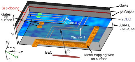
We consider an atom chip built on a GaAs/(AlGa)As heterojunction, which traps a BEC near a 2DEG (Fig. 1). In the first part of the paper, the trapping potential is produced by currrent, , through a Z-shaped metal surface wire (yellow in Fig. 1), combined with a uniform magnetic field , which positions the trap center at distance from conducting Channel 1 in the 2DEG wil . The 2DEG is formed by electrons from ionized donors in a Si -doping layer (red in Fig. 1) Buks et al. (1994); Grill and Döhler (1999), which migrate into the GaAs and populate the ground state of an almost triangular potential well formed at the GaAs/(AlGa)As interface pep ; Grill and Döhler (1999). This confines the electrons in a narrow ( 15 nm thick) sheet (blue in Fig. 1). Insulating regions in the 2DEG (gray in Fig. 1), made by implanting Ga ions Ensslin and Petroff (1990), enclose two distinct conduction channels, labelled 1 and 2 in Fig. 1.
Atom chips are usually built on a bulk substrate, which generates strong CP attraction, thus preventing atoms from being trapped closer than a few m from the surface Lin et al. (2004). Recently, suspended trapping wires were used to reduce the CP potential mul . We consider a heterojunction membrane of width 130 nm, as in recent experiments Bli , and calculate the CP potential energy [, where Jm4] via Eqs. (25-29) of ebe . As shown below, is weak enough to allow submicron trapping.
We take typical heterojunction parameters with ionized donors at distance nm from the 2DEG (Fig. 1) Judd et al. (2010); Efros et al. (1993). The 2DEG is nm below the surface and of mean electron density equal to . Since the 2DEG is so thin, surface fluctuations are negligible: a major advantage over metal wires for near-surface trapping. We take the heterojunction temperature to be K (as in superconducting atom chips sup ) to ensure high 2DEG conductivity, , and that inhomogeneity in the current originates only from non-uniformity of the ionized donors Buks et al. (1994); Grill and Döhler (1999).
These donors create a spatially-varying attractive potential, which is partially screened by the 2DEG pep . In the Thomas-Fermi screening model Efros et al. (1993), the potential energy of a 2DEG electron at position is
| (1) |
where , , is the 2D Fourier transform of the spatial ionized donor density, , is the relative permittivity of GaAs, and the screening wave vector, , depends on the electron charge, , and effective mass, Efros et al. (1993).
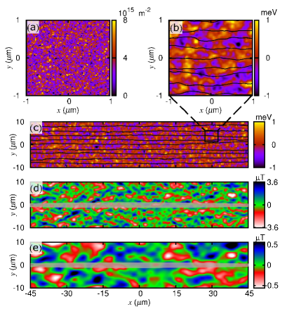
We now consider the electrostatic properties and current profile of Channel 1, whose width is henceforth taken to be . Figure 2 shows (a) a typical uncorrelated ionized donor distribution, , and (b,c) the screened potential energy in the 2DEG, Coleridge (1997).
When an applied voltage creates an electric field, E, along Channel 1, the local current density is str , where the inhomogenous component originates from fluctuations in and .
The black curves in Fig. 2(b,c) show current streamlines calculated for kVm-1. Imhomogeneity of makes these streamlines deviate from the direction. Consequently, the resulting magnetic field at position in the plane has a non-zero component given, from the Biot-Savart law Roth et al. (1989); str , by
| (2) |
where is the 2D Fourier transform of the donor density fluctuations, . Equation (2) reveals two key results. First, the fluctuations of depend directly on the donor distribution via . Second, due to the term, the field fluctuations become weaker and smoother as increases. This can be seen by comparing the color maps of in Fig. 2(d,e).
We now consider how the field fluctuations affect a BEC, henceforth called BEC A, comprising 87Rb atoms in state , whose position in the plane is shown by the gray regions in Fig. 2(d,e). Since the BEC is strongly confined along and , its density profile is sensitive only to fluctuations in . Along the axis [], the atom density fluctuations are wil , where the g-factor , is the Bohr magneton, is the trap frequency in the plane and is the s-wave scattering length.
The variation of the oscillatory amplitudes of with is crucial for understanding, and exploiting, the effect of 2DEG current on a BEC. To demonstrate this, we first consider the rms average, , of along at given . If the spatial donor correlation function, , is homogeneous along and as , the rms spatial average is equivalent to an ensemble average, denoted , at any given . Choosing gives
| (3) |
Equation (3) reveals that depends on, and can hence probe, the correlation function of the ionized donors, , in k-space.
For a random donor distribution (Fig. 3 right inset) Coleridge (1997), . Using this in Eq. (3) gives (solid curve in Fig. 3), meaning that for m, field fluctuations decay more slowly above a 2DEG than above a metal wire (dot-dashed curve in Fig. 3, calculated for a wire of width using formulae and parameters for surface and edge roughness from Schumm et al. (2005)). As a result, the BEC responds to field fluctuations over a range of , with an upper limit m where falls too low to detect ( of the mean atom density Aigner et al. (2008)), and a lower limit nm determined by (see below). The form of gives information about donor correlations in this range.
Both and can be determined directly from measurements of made by scanning the BEC over the 2DEG at fixed , which sets the resolution Roth et al. (1989); wil ; Hall et al. (2007); Aigner et al. (2008). As shown in wil , a Fourier transform of gives : follows from current continuity, thence from integrating . Finally, deconvolving the relation between and stated in Efros et al. (1993), using the method in wil , gives , , and . For m, the resolution is sufficient to image, for example, electron redistribution during metal-insulator transitions Ilani et al. (2001); Grill and Döhler (1999) and, in particular, m-scale ionized donor correlations in high mobility 2DEGs MacLeod et al. (2009); Umansky et al. (2009); Siegert et al. (2007). Donor statistics are of fundamental importance to electron transport and mobility Buks et al. (1994); Coleridge (1997); Grill and Döhler (1999); Koonen et al. (2000); Topinka et al. (2001), but usually inferred from theoretical models due to a lack of non-invasive experimental probes Grill and Döhler (1999); Topinka et al. (2001). Scanning probe methods can image 2DEGs on the nm scale over a few m2. In contrast, BEC microscopy offers non-invasive, fast (single-shot) imaging of and over large (100s of m2) areas of the 2DEG. So it is ideal for imaging, in situ, long-range donor correlations, which are the key to enhancing mobility, and their response to illumination or thermal cycling.

The ionized donor profile, and hence , can be permanently changed by transient optical illumination Koonen et al. (2000). Since the ionized donor density increases with the local light intensity, two laser beams, of wavelength , counter-propagating along , spatially modulate the donor profile with a period (Fig. 3 left inset). In this case, , where . Using this in Eq. (3) gives , shown for 660 nm by the dotted curve in Fig. 3. This rapid decay occurs because, as in a magnetic mirror Hinds and Hughes (1999), the current streamlines align with the striped donor pattern (Fig. 3 left inset), which reduces their meander and, hence, .
The ability to tailor the potential landscape of the 2DEG, and the resulting field fluctuations, is a unique feature of heterojunctions, which can be exploited for trapping, manipulating, and imaging with, ultracold Bose gases. Crucially, exponential decay makes the curve for the periodically-modulated donor distribution (dotted in Fig. 3) fall rapidly below that for a metal wire (dot-dashed curve in Fig. 3). At m, the field fluctuations above the 2DEG are more than 3 orders of magnitude smaller than for the metal wire.
Consequently, 2DEGs have great potential for creating near-surface microtraps. To demonstrate this, we consider the trap produced by a 355A current through 2DEG Channel 1 (of width m and central arm length m) only, setting . The solid curve in Fig. 4(a) shows the total potential energy calculated for an 87Rb atom, where originates from the magnetic field produced by Channel 1 and an applied field mG. Since the CP attraction is weak, the trap is deep enough to confine BEC B, comprising 87Rb atoms with , whose chemical potential [horizontal line in Fig. 4(a)] is far below the top of the left-hand barrier. Even though the trap center is only m from the 2DEG [Fig. 4(a)], varies fairly smoothly with [solid curve in Fig. 4(b)] because is only nT (Fig. 3). Even at 4.2 K, the resistance of Channel 1 is 10 times higher than a similarly-sized gold conductor at room temperature Salem et al. (2010). Consequently, 2DEGs offer lower Johnson noise and spin-flip loss rates than metal wires.
Near-surface trapping makes the BEC highly sensitive to magnetic field variations arising from the geometry of the conduction channels, such as local narrowing. As an example, suppose that B is adjusted to hold BEC B across the middle arm of U-shaped Channel 2 [Figs. 1 and 4(b) inset]. Channel 2 is narrow enough (20 nm) for the electrons to populate a small number, , of discrete energy levels, (), corresponding to motion across it. Along the channel, whose quantized conductance is pep ; Koonen et al. (2000), electrons occupy one-dimensional plane wave states up to the Fermi level, . Applying a negative voltage, , to metal surface gates (yellow rectangles in Fig. 1), which are on either side of the lower arm of Channel 2 and sufficiently far from the BEC to have negligible electrostatic effect on it, locally depletes the 2DEG. This narrows the conduction channel, forming a QPC and raising . As increases, the energy levels successively exceed and depopulate pep ; Koonen et al. (2000); Topinka et al. (2001). Depopulation of each level decreases and, hence, the current through Channel 2 by , where is the voltage dropped across the QPC.
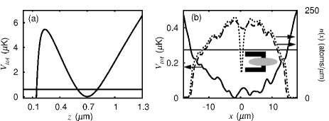
The dashed curve in Fig. 4(b) shows the density profile, , of BEC B when the QPC in Channel 2 is fully depleted (). Since the QPC carries no current in this case, is the unperturbed ground state of the trapping potential shown by the solid curves in Fig. 4(a,b). Opening a single conduction channel in the QPC () changes the trap profile sufficiently to almost completely split the BEC [dotted curve in Fig. 4(b)]. Consequently, the BEC can detect quantized changes in the QPC’s conductance, which, conversely, can manipulate the BEC, for example splitting and recombining it in atom interferometry. More complex shaping of the atom cloud is also possible: an array of QPCs could imprint and control a wide range of sub-m patterns in the BEC.
In summary, quantum electron transport in heterojunctions can create smooth, low-noise, magnetic traps, which provide the sub-m control required to integrate ultracold atoms with quantum electronic systems. By tailoring the donor distribution, magnetic field fluctuations can be suppressed exponentially. Quantum transport processes in a 2DEG can imprint strong density modulations in a BEC, which, conversely, provide a non-invasive probe of those processes. The ability to measure the potential landscape and mobility of a 2DEG independently may yield new insights for understanding how the two relate and, hence, for increasing 2DEG mobility MacLeod et al. (2009); Umansky et al. (2009). Suspended graphene membranes, which combine low CP attraction with high room-temperature mobility Geim (2009), could be the ultimate material for sub-m atom trapping and BEC microscopy of quantum transport.
References
- (1) For reviews see: J. Reichel, Appl. Phys. B: Lasers Opt. 74, 469 (2002); R. Folman et al., Adv. At. Mol. Opt. Phys. 48, 263 (2002); J. Fortágh and C. Zimmermann, Rev. Mod. Phys. 79, 235 (2007).
- Hinds and Hughes (1999) E. A. Hinds and I. G. Hughes, J. Phys. D 32, R119 (1999).
- Aubin et al. (2006) S. Aubin et al., Nature Physics 2, 384 (2006).
- (4) T. Schumm et al. Nature Physics 1, 57 (2005); G.-B. Jo et al., Phys. Rev. Lett. 98, 180401 (2007).
- Hall et al. (2007) B. V. Hall et al., Phys. Rev. Lett. 98, 030402 (2007).
- (6) Some magnetic sensors use optical traps: M. Vengalattore et al., Phys. Rev. Lett. 97, 200801 (2007).
- Roth et al. (1989) B. Roth, N. Sepulveda, and J. Wikswo, J. Appl. Phys. 65, 361 (1989).
- (8) S. Wildermuth et al., Nature 435, 440 (2005); Appl. Phys. Lett. 88, 264103 (2006).
- Aigner et al. (2008) S. Aigner et al., Science 319, 1226 (2008).
- (10) T. Mukai et al., Phys. Rev. Lett. 98, 260407 (2007); C. Roux et al., Eur. Phys. Lett. 81, 56004 (2008).
- (11) K.-F. Berggren and M. Pepper, Phil. Trans. R. Soc. A 368, 1141 (2010), and Refs. therein.
- Geim (2009) A. K. Geim, Science 324, 1530 (2009).
- Judd et al. (2010) T. E. Judd et al., New J. Phys. 12, 063033 (2010).
- Hammes et al. (2003) M. Hammes et al., Phys. Rev. Lett. 90, 173001 (2003).
- Allwood et al. (2006) D. A. Allwood et al., Appl. Phys. Lett. 89, 014102 (2006).
- Henkel (2005) C. Henkel, Eur. Phys. J. D 35, 59 (2005).
- Sinclair et al. (2005) C. Sinclair et al., Phys. Rev. A 72, 031603(R) (2005).
- Lin et al. (2004) Y. Lin et al., Phys. Rev. Lett. 92, 050404 (2004).
- Wang et al. (2004) D.-W. Wang, M. D. Lukin, and E. Demler, Phys. Rev. Lett. 92, 076802 (2004).
- Krüger et al. (2007) P. Krüger et al., Phys. Rev. A 76, 063621 (2007).
- Fortágh et al. (2002) J. Fortágh et al., Phys. Rev. A 66, 041604 (2002).
- Jones et al. (2003) M. P. A. Jones et al., Phys. Rev. Lett. 91, 080401 (2003).
- Estève et al. (2004) J. Estève et al., Phys. Rev. A 70, 043629 (2004).
- Trebbia et al. (2007) J. B. Trebbia et al., Phys. Rev. Lett. 98, 263201 (2007).
- (25) E.M. Höhberger et al., Appl. Phys. Lett. 82, 4160 (2003).
- Buks et al. (1994) E. Buks, M. Heiblum, and H. Shtrikman, Phys. Rev. B 49, 14790 (1994).
- Coleridge (1997) P. T. Coleridge, Semicond. Sci. Technol. 12, 22 (1997).
- Grill and Döhler (1999) R. Grill and G. H. Döhler, Phys. Rev. B 59, 10769 (1999).
- Koonen et al. (2000) J. J. Koonen, H. Buhmann, and L. W. Molenkamp, Phys. Rev. Lett. 84, 2473 (2000).
- Topinka et al. (2001) M. A. Topinka et al., Nature 410, 183 (2001).
- Schumm et al. (2005) T. Schumm et al., Eur. Phys. J. D 32, 171 (2005).
- Ensslin and Petroff (1990) K. Ensslin and P. M. Petroff, Phys. Rev. B 41, 12307 (1990).
- (33) H.-C. Chuang et al., Sens. Actuators A: Phys. (2010), doi:10.1016/j.sna.2010.01.003.
- (34) A. M. Contreras Reyes and C. Eberlein, Phys. Rev. A 80, 032901 (2009).
- Efros et al. (1993) A. L. Efros, F. G. Pikus, and V. G. Burnett, Phys. Rev. B 47, 2233 (1993).
- (36) Assuming E is large enough for to weakly perturb the current streamlines. Atom density fluctuations then result only from and are thus independent of E.
- Ilani et al. (2001) S. Ilani et al., Science 292, 1354 (2001).
- MacLeod et al. (2009) S. J. MacLeod et al., Phys. Rev. B 80, 035310 (2009).
- Umansky et al. (2009) V. Umansky et al., J. Crystal Growth 311, 1658 (2009).
- Siegert et al. (2007) C. Siegert et al., Nature Physics 3, 315 (2007).
- Salem et al. (2010) R. Salem et al., New J. Phys. 12, 023039 (2010).