Atom chips on direct bonded copper substrates
Abstract
We present the use of direct bonded copper (DBC) for the straightforward fabrication of high power atom chips. Atom chips using DBC have several benefits: excellent copper/substrate adhesion, high purity, thick (m) copper layers, high substrate thermal conductivity, high aspect ratio wires, the potential for rapid ( hr) fabrication, and three dimensional atom chip structures. Two mask options for DBC atom chip fabrication are presented, as well as two methods for etching wire patterns into the copper layer. The wire aspect ratio that optimizes the magnetic field gradient as a function of power dissipation is determined to be 0.84:1 (height:width). The optimal wire thickness as a function of magnetic trapping height is also determined. A test chip, able to support 100 A of current for 2 s without failing, is used to determine the thermal impedance of the DBC. An assembly using two DBC atom chips to provide magnetic confinement is also shown.
pacs:
03.75.Be, 37.10.Gh, 41.20.GzAtom chips have been used in many cold atomic physics experiments including magneto-optical traps Reichel et al. (1999), magnetic traps Weinstein and Libbrecht (1995); Reichel et al. (1999), waveguides Müller et al. (1999); Luo et al. (2004), transports Hänsel et al. (2001a); Günther et al. (2005), Bose-Einstein condensates Hänsel et al. (2001b), coherent and incoherent beam splitters Cassettari et al. (2000); Schumm et al. (2005); Shin et al. (2005), and have been integrated with optical elements Wang et al. (2005); Teper et al. (2006); Purdy and Stamper-Kurn (2008). Using atom chips for cold neutral atom physics has two main advantages. First, by manipulating atoms from the chip wires, high magnetic field gradients can be generated at low power dissipation ( W). Second, by using well established lithographic fabrication techniques atom chip wires can be precisely placed to generate well defined magnetic fields.
For many applications, e.g. atom interferometry using light pulses, working distances of several hundred microns are common. As shown in Appendix A, power dissipation of a magnetic trap is minimized when the working distance from the top surface of a rectangular wire is and when the aspect ratio is , where is the thickness and is the width of the wire. Realization of thick high quality metalizations with standard lithographic techniques has proven to be technologically challenging, time consuming, and very expensive. For atom chip based magnetic traps that require working distances , we present the use of direct bonded copper (DBC) substrates for atom chip fabrication.
Direct bonded copper is the direct joining of a thin sheet of pure copper to a ceramic substrate Burgess and Neugebauer (1975) and is commonly used in power electronics due to its high current handling and heat dissipation properties. Using DBC for atom chips addresses several atom chip fabrication requirements including power dissipation, ease of fabrication, thick metalizations, and excellent wire adhesion. The power dissipation of DBC atom chips is reduced for two reasons. First, thick, pure copper layers are readily available for DBC substrates with a resistivity equal to bulk copper. Second, the ability to easily produce thick atom chip wires that have a reduced net resistance. Another benefit of using DBC for atom chips is the potential for rapid in-house fabrication with minimal equipment. We have produced moderate quality atom chips in less than eight hours, and high quality wires in approximately one week with most of the time being taken by mask design and printing. By using DBC it is straightforward to fabricate various rectangular wire cross sections or aspect ratios because of the availability of a thick copper layer. Wires with aspect ratio can be fabricated by wet etching, and it may be possible to realize high aspect ratio wires using ablative laser micro-machining Karnakis et al. (2005).
To date, most atom chips have been fabricated using a Damscene process, where the wire height and aspect ratio are determined by the photoresist thickness and the metal deposition (electroplating or evaporation) with typical wire heights on the order of Fortagh et al. (1998); Reichel et al. (2001); Drndić et al. (1998); Estève et al. (2004); Groth et al. (2004); ju Lin et al. (2004); Horikoshi and Nakagawa (2006). Thick lithographic wires have been fabricated using thick photoresists Müller et al. (1999) or by depositing metal in channels formed in the substrate (e.g. deep reactive ion etching in silicon) but the difficulty of fabrication has made thick wires less common. The thickness of a DBC layer is variable but is commonly as thick as 200 for high current applications.
Wire substrate adhesion is another key consideration when fabricating atom chips and this is especially true for thick wires because residual stress from metalization increases the probability of delamination. This problem is most often manifest after the atom chip has been fabricated and is being prepared for use. While this is a technological problem with a known solution (i.e. careful surface preparation) it is a frequent issue that is solved by using DBC. In our experience, it takes considerable effort to remove the copper from the substrate which has made it possible to perform significant post processing of the atom chip. For example, we have mechanically removed selected areas of the ceramic substrate after the copper has been etched so that the chip can be folded to yield a three dimensional “origami chip”.
In this paper we will discuss basic fabrication methods, the resulting wire quality, and power dissipation. We will show DBC atom chips that are post-processed to make three dimensional chip structures that simplify electrical connections to the atom chip.
I Fabrication of Atom chips using Direct Bonded Copper
To make DCB substrates, a copper sheet and a ceramic are bonded using the oxygen-copper eutectic ( 1.5% oxygen at ) that is just below the melting point of pure copper (). During bonding, a thin melt layer occurs at the oxide-copper interface that wets the ceramic surface and fills surface irregularities. The resulting bond is very strong because of the surface wetting between the copper and the oxide, and has excellent thermal conductivity because the intermediate liquid stage fills voids between the copper and the substrate. During bonding, the melt layer solidifies as diffusion of copper and oxygen at the interface moves the stoichiometric composition of the melt away from the eutectic transition. To provide enough oxygen for the eutectic transition, a thin ceramic oxide layer on the surface of the copper and ceramic is required. The substrate can be an oxide (e.g. aluminum oxide () or Beryllium oxide (BeO)) or the surface can be oxidized prior to bonding (e.g. formation on aluminum nitride (AlN) or copper oxide on copper), however, the surface oxidation step can reduce the bulk thermal conductivity due to the diffusion of oxygen along grain boundaries Sheng and Colino (2004).
While any oxide can be used for DBC, most applications use electrically insulating substrates that are thermally conductive. Beryllium oxide has the highest thermal conductivity () of the ceramics, but is not commonly used because of beryllium toxicity. Most DBC substrates are or AlN. Aluminum oxide is commonly used despite a moderate thermal conductivity () because of its low cost, high substrate quality, and high bond strength. Aluminum nitride is also used because of its high thermal conductivity () and a coefficient of thermal expansion () that is closely matched to silicon.
Aluminum nitride has previously been used for atom chips with electroplated wires Reichel et al. (1999) where the wires are in direct and conformal contact with the substrate, however, electroplated metals typically have higher resistivities than the bulk metal and, as a result, the maximum current density is reduced Teh et al. (2001). Additionally, electroplated metals have a grained structure that results in variations of the magnetic field close to the wire Estève et al. (2004). In DBC, the bonded copper maintains the electrical properties of the original copper sheet (i.e. high purity, high density, and low resistivity) for all thicknesses of DBC. The high purity of the DBC permits high total currents relative to electroplated wires of the same thickness Sheng and Colino (2004), or for the same current reduced power dissipation. Pure and high density atom chip wires have been deposited via evaporation with bulk resistivity and smooth wire edges Groth et al. (2004). The evaporation process is suitable for thin films () but is complicated (e.g. refilling the evaporation source) and inefficient because only a small fraction of the evaporated metal is deposited on the substrate while the remainder sticks to the walls of the vacuum system.
Excellent wire to substrate adhesion is a significant practical benefit of DBC atom chips. Atom chips that use electroplated or evaporated wires need an adhesion layer (e.g. Ti, TiW, Cr) to avoid delamination of the atom chip wires. The quality of the adhesion can vary significantly and depends on substrate cleanliness, deposition parameters, and substrate compatibility. Wire adhesion is especially important for thicker wires that may have residual stress from the growth process. The adhesion of DBC is excellent; it takes significant force to remove bulk copper or thin wires from the substrate. Because of the excellent adhesion, atom chips can be modified after patterning (see Sec. II) while maintaining the integrity of the rest of the atom chip.
High current hermetic vias is another option made possible by DBC and is a standard option for DBC substrates Schulz-Harder and Exel (2003) and have been used as a part of a neutral atom trap Wang et al. (2007). Commercially available vias are incorporated into the substrate during the bonding process and require a custom manufacturing run. It may also be possible to form vias by drilling through the substrate and soldering or electroplating in the hole to form a via.
Although there are many potential methods for building a DBC atom chip, the chips in this paper are fabricated by applying a mask to the surface of the DBC and then etching the copper away from the exposed areas leaving wire traces on the AlN substrate. For rapid prototyping (several hours), laser printer toner is used for the mask and the copper is etched with hydrochloric acid plus dilute hydrogen peroxide. For thick copper this method can reproducibly produce wide wires with center to center spacing. The minimum feature size is determined by the resolution of the laser printer and the thickness of the copper. The second fabrication method uses photoresist and a commercially printed mask with sub-micron resolution. After the pattern transfer, using standard lithographic procedures, the wires are etched using either hydrochloric/peroxide or reverse electroplating Liu (2001). For thick copper this method can reproducibly produce wires widths of with spacing. With care wire widths of with spacing can be fabricated. Specific processing details of each method follow below.
To promote mask adhesion, the DBC surface is first cleaned by scrubbing the surface with steel wool and then rinsing with acetone and methanol. For rapid mask production, laser printer toner provides a chemically resistant thermo-plastic that adheres to a surface when it is melted. The toner may be remelted for multiple transfers between different substrates. A 600 dpi laser printer is used to print the chip design onto a commercially available PCB transfer film 111An HP LaserJet printer was used for printing the mask. Press-n-Peel and Pulsar toner transfer papers have been used with similar success. Specific vendors are provided for information only and does not constitute endorsement.. The transfer film will release the backing at the areas where the toner sticks to the DBC making it possible to remove the original printing media. The toner transfer procedure follows the manufacturer’s instructions with special care given to the temperature cycling because overheating will result in a distorted toner mask. After etching, the mask is removed with acetone. The advantage of the toner transfer mask is rapid mask production with minimal equipment. The feature size using toner transfer is limited by the printer resolution, the spreading of the toner during transfer, and the DBC thickness.
Improved mask quality and smaller wires are achieved using photolithography. First, a silicon nitride layer is applied to the DBC to improve photoresist adhesion. A photoresist layer (AZ4620 or SU8) is spin coated and then lithographically patterned. Compared to the toner transfer method, the photolithographically defined atom chip wires are significantly straighter and the achievable wire width is significantly narrower (). The sidewall definition and minimum line size is a strong function of the total copper thickness. For the thick DBC used in this paper, the narrowest line feature that could be reproducibly etched was (). Compared to a toner transfer produced atom chip a lithographically produced atom chip requires more time (multiple days versus hours) and additional equipment, but is able to produce finer features, more consistent lines, and accurate wire placement not possible using a toner mask.
Several test chips were etched using solutions of 37% hydrochloric acid (HCl), hydrogen peroxide, and water in a mixture of approximately 5:1:10 by volume. The wire quality depended on the peroxide concentration, etching time, and solution agitation. The hydrogen peroxide concentration was varied from 2 to 0.2 by volume, with lower concentrations yielding longer etching times (1-2 hrs) and the best wires. Solution agitation reduces the etch times by removing bubbles from the surface and provides fresh chemicals to the etching areas. At the end of the etching procedure a pipette was used to provide local agitation to reduce wire footing and assure electrical isolation of the atom chip wires. For low concentrations of hydrogen peroxide (0.4 by volume) no agitation is necessary because of reduced surface bubbles. The acid/hydrogen peroxide etching method is isotropic and causes undercutting of the mask, resulting in a trapezoidal wire shape and a wire width that is smaller than the original mask.
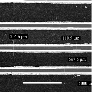
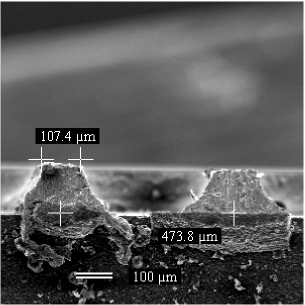
The quality of various masking and etching methods was investigated by varying wire widths and spacings. The resulting quality of the etching processes and masking methods were quantified using a scanning electron microscope. Two test chips are presented below and are representative of the photolithographically defined process. Figures 1 and 2 are top and cross sectional views of test chip A. This chip was fabricated using a photoresist mask (Hoechst AZ4620) that consisted of equally spaced wide traces on thick DBC on AlN. The copper was etched using a concentration of hydrogen peroxide of 1.2 parts by volume and the etching took about 15 min. As shown in Fig. 1, the traces produced by this method are straight, parallel, and the dimensions of each trace are nearly identical. The footing of the wire is less uniform than the top of the wire because of varying etch rates at the end of the etching process. Figure 2 is a cross sectional view of test chip A that shows a trapezoidal shape that is the result of the wet etching process used. The width of the traces at the bottom is about and the width at the top of the trace is about . The wet etch process used caused undercutting of approximately from each side of the mask. The aspect ratio of these wires is about .
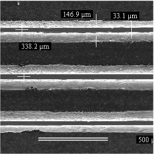
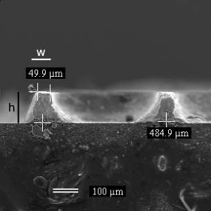
Figures 3 and 4 are electron micrographs of test chip B. This chip was made using the same substrate as test chip A, however, the hydrogen peroxide concentration was reduced to 0.6 parts by volume and the wire mask widths were . The etching of this chip took about 30 min. Similar to the wide traces, Fig. 3 shows the wide traces are also straight, parallel and reproducible. Figure 4 shows that for this chip, the traces have straighter sidewalls and less undercutting than observed in test chip A. This is attributed to the lower concentration of hydrogen peroxide. The width of the top of these wires was about yielding an aspect ratio of .
Test chips were also fabricated using reverse electroplating. The DBC with applied photoresist mask was fixed parallel to a blank, similar sized piece of copper and suspended in a copper sulfate solution with brighteners 222Available from McMaster-Carr. This is provided only as information and is not an endorsement.. A positive voltage was applied to the atom chip which removed copper from the unmasked areas which was then deposited on the blank copper. Low current densities (0.5 A/m2) produced the best results, but resulted in increased etching times. A magnetic stirrer was used to provide fresh solution to the surface of the DBC, however, for long etching times the photoresist mask debonded because of the constant agitation of the electroplating solution. Toward the end of the reverse electroplating, small (m diameter) copper islands remain because they were no longer electrically connected. The copper islands were removed by a rapid ( min) acid etch. While reverse electroplating has the potential to provide higher aspect ratio wires and close wire placement, the limits of the process are not determined at this time because of the mask integrity.
The maximum current handling and the thermal impedance of DBC atom chips was tested by fabricating a test chip with three long wires with different widths: , , and . To approximate the reduced thermal dissipation in vacuum, the chip was tested in air without a heat sink . Only the results of the thinnest wire are reported because the heating effects were found to be negligible for the wider wires. The heating (measured using a thermocouple on the substrate 5 mm from the wire) and the voltage drop across the wire were measured for currents of 10-100 A ( A/m2). A 2 s current pulse of 100 A (110 W average power) resulted in a 2.7 times increase in the wire resistance and ℃ temperature rise. For short times ( ms) the thermal conductance of the wire/substrate junction was measured to be W/K-m2, which is approximately 1.5-2 times the wire/substrate junction thermal conductance of silicon with a 20 nm oxide layer Groth et al. (2004). With a suitable heat sink the DBC atom chips should have equal or better performance in vacuum.
II Assembly

a.)
 b.)
b.)
 c.)
c.)
 d.)
d.)
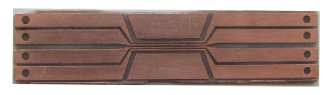
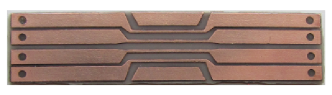
We are currently developing a trapped atom interferometer gyroscope Stickney et al. (2009) that uses a cigar shaped harmonic trap. Our plan is to realize this trap using a two layer DBC atom chip. The chips were fabricated using a toner transfer mask and a HCl/peroxide etch. The chip closest to the atoms (front chip) has four parallel wires that are wide and spaced center to center. Figure 5a shows the mask and Fig. 5b is a photograph of the final front chip. The chip farthest from the atoms (back chip) has four parallel wires that are wide and are separated by . The mask and chip for are shown in Figs. 5 c and d. Areas of the chip that would otherwise be open are filled to reduce the amount of etchant used and to maintain a level top surface. The chip wire leads are 2.5 mm wide to reduce power dissipation and provide strength when the substrate is removed in later processing.
After the atom chips were etched the substrates were modified for making electrical connections by drilling holes 333We have use diamond drill bits from Dad’s Rock Shop and diamond plated grinding bits from McMaster-Carr. This is not an endorsement and is for information only. at the end of the chip. To improve optical access and to accommodate the space requirements, the edges of the chip were folded back so the electrical connections could be made behind the mounting structure. To avoid stressing and breaking the copper at the bend areas, the AlN substrate was removed with a diamond grinding bit that is 2-3 times wider than the substrate thickness. This is a straight forward and reliable process because the diamond bit removes hard material significantly faster than soft materials (i.e. the AlN can be removed without damaging the copper). The copper traces were deformed by the slight pressure of the diamond grinding bit but have no noticeable degradation in performance. This processing was made possible due to the excellent adhesion of the copper to the substrate and the copper thickness that is readily available using DBC. This can also be accomplished by bonding multiple substrates with appropriate gaps, however this requires minimum lot runs and is not practical for one-off atom chip designs.
Perhaps the main advantage of foldable atom chips (dubbed “origami chips”) is that they permit potentially bulky electrical connections to be made away from the surface of the atom chip. This allows direct connections to be made to the chip while maintaining optical access over the full range of the chip. High power electrical connections are available to the chip without bond wires, soldering, or vias. The effect of the leads can be easily taken into account because the wires have a well defined path away from the chip.
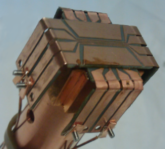
Figure 6 is a photograph of a DBC atom chip assembly constructed using two atom chips, shown in Fig. 5, that were processed, folded, stacked, and epoxied to a copper heat sink (using Epotek 353 ND). Four of the wires were connected using vacuum compatible screws. The assembly was placed in an UHV chamber and baked at ℃ for approximately one week. After bakeout, the UHV chamber was isolated from the turbo pump and was pumped solely by a 40 l/s ion pump to a final pressure of torr. A 87Rb MOT was loaded directly below the DBC atom chip assembly and was then compressed and cooled in a compressed MOT. The atoms were magnetically trapped and transported to the DBC atom chip where they were transferred to a chip quadrupole magnetic trap made by running current in the front chip wire plus an appropriate bias field. The ability to quantify the quality of the first chip was limited by the optical quality of the glass vacuum chamber. A new vacuum chamber has been constructed to address the optical quality issues.
III Conclusion
Direct bonded copper substrates are an excellent candidate for atom chip fabrication because of thick high purity copper that is intimately bonded to a high thermal conductivity substrate. Direct bonded copper atom chips can support very high currents (at minimum 100 A) for several seconds for high magnetic field gradient traps or for reduced power dissipation at lower currents. Wires with the appropriate cross section will further optimize the magnetic field gradient for a given power dissipation. The fabrication of DBC atom chips is straight forward and requires very little equipment. Direct bonded copper atom chips are very robust and can be bent to form 3D atom chip structures that simplifies the electrical connections away from the chips or for precision wire placement in multiple dimensions.
While this paper demonstrates the initial design and use of DBC for atom chips, there are multiple avenues for future improvements, such as, other copper patterning techniques (laser etching or dry etching Lee et al. (1998)) which could produce higher density and/or higher aspect ratio wires. Additionally, high precision and high current coils can be made for precise generation of centimeter size magnetic fields. The DBC can also be patterned as a thermally conductive carrier for atom chips with finely patterned lithographic wires Günther et al. (2005). The ability to form vias in the DBC also allows for greater flexibility in chip designs and for the potential to make high power hermetic feedthroughs.
Acknowledgements.
This work was funded under the Air Force Office of Scientific Research under program/task 2301DS/03VS02COR.Appendix A Optimal wire aspect ratio
To determine the optimal aspect ratio that minimizes the power dissipated by a wire, consider the magnetic field produced by a rectangular wire with height and width that carries current in the -direction. In addition to the field produced by the rectangular wire, there is a uniform bias field applied in the -direction, such that there is a minimum in the field along the line , . Near this point, the magnitude of the magnetic field is
| (1) |
and the magnetic field gradient is
| (2) |
where is the current density in the wire.
In a typical experiment, the magnetic field gradient is set at a particular value. For example, in evaporative cooling, the magnetic field must be large enough that the collision rate is high, but no so high that three body collisions limit the lifetime of the trapped atoms. Additionally, in chip experiments the distance from the center of the trap to the chip is made as small as possible. The minimum distance is typically chosen to avoid fragmentation, the Casimir-Polder effect ju Lin et al. (2004), thermal noise, or for optical access in atom interferometry experiments. Thus, the remaining task is to determine the height and width of a wire that minimizes the power dissipation for a given magnetic field gradient and working distance .
The power dissipated by the current carrying wire is
| (3) |
where is the resistivity and is the length of the wire. Combining Eq. (2) and Eq. (3) the dimensionless magnetic field gradient as a function of power dissipation can be written
| (4) |
where is the aspect ratio of the wire, is the ratio of the trapping distance to the wire thickness and
| (5) |
is the power dissipated by the wire. Equation (5) shows that the power dissipation is minimized when is maximized.
Analysis of Eq. (4) shows that for each value of , there is a value of that maximizes the . Figure 7 shows the optimal value of as a function of . When , the optimal aspect ratio is larger than one, which means that when the trap is closer to the wire than the thickness of the wire. This is because the magnetic field and corresponding gradient near a broad wire is constant. In order to avoid the effects of a broad wire, the wire aspect ratio must be greater than approximately one. On the other hand, when , the optimal aspect ratio is smaller than one because the magnetic trap is far enough away to avoid the flattening of the magnetic field and the wider wire will result in a reduced wire resistance.
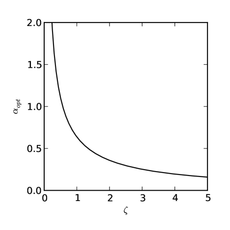
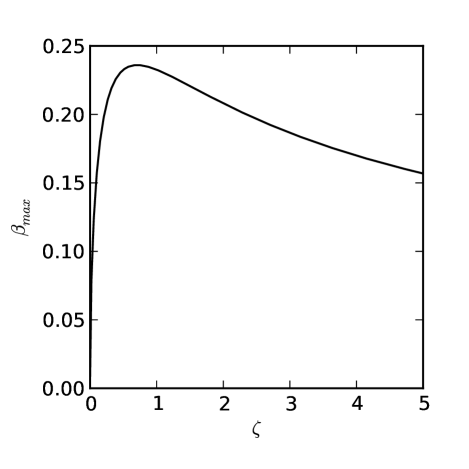
Figure 8 shows the maximum value of as a function of . When the maximum value of decreases rapidly reaching when . Since the power dissipation is , the minimum power dissipation rapidly increases as the trap is brought close to the wire. When , the maximum value of decreases, meaning that the minimum power dissipation increases as the trap is moved far away from the wire. When and the power dissipation reaches a global minimum with .
As an example, consider the first BEC on a chip Hänsel et al. (2001b) achieved using m gold wires electroplated on an AlN substrate. The atoms were trapped m from the chip surface. Thus, , , and using Eq. (4) . For an optimal wire with and with the same field gradient and trapping distance can be achieved while dissipating 0.3 times the power.
References
- Reichel et al. (1999) J. Reichel, W. Hänsel, and T. W. Hänsch, Phys. Rev. Lett. 83, 3398 (1999).
- Weinstein and Libbrecht (1995) J. D. Weinstein and K. G. Libbrecht, Phys. Rev. A 52, 4004 (1995).
- Müller et al. (1999) D. Müller, D. Z. Anderson, R. J. Grow, P. D. D. Schwindt, and E. A. Cornell, Phys. Rev. Lett. 83, 5194 (1999).
- Luo et al. (2004) X. Luo, P. Krüger, K. Brugger, S. Wildermuth, H. Gimpel, M. W. Klein, S. Groth, R. Folman, I. Bar-Joseph, and J. Schmiedmayer, Opt. Lett. 29, 2145 (2004).
- Hänsel et al. (2001a) W. Hänsel, J. Reichel, P. Hommelhoff, and T. W. Hänsch, Phys. Rev. Lett. 86, 608 (2001a).
- Günther et al. (2005) A. Günther, M. Kemmler, S. Kraft, C. J. Vale, C. Zimmermann, and J. Fortágh, Phys. Rev. A 71, 063619 (2005).
- Hänsel et al. (2001b) W. Hänsel, P. Hommelhoff, J. Reichel, and T. W. Hänsch, Nature 413, 498 (2001b).
- Cassettari et al. (2000) D. Cassettari, B. Hessmo, R. Folman, T. Maier, and J. Schmiedmayer, Phys. Rev. Lett. 85, 5483 (2000).
- Schumm et al. (2005) T. Schumm, S. Hofferberth, L. M. Andersson, S. Wildermuth, S. Groth, I. Bar-Joseph, J. Schmiedmayer, and P. Kruger, Nat Phys 1, 57 (2005).
- Shin et al. (2005) Y. Shin, C. Sanner, G.-B. Jo, T. A. Pasquini, M. Saba, W. Ketterle, D. E. Pritchard, M. Vengalattore, and M. Prentiss, Phys. Rev. A 72, 021604 (2005).
- Wang et al. (2005) Y.-J. Wang, D. Z. Anderson, V. M. Bright, E. A. Cornell, Q. Diot, T. Kishimoto, M. Prentiss, R. A. Saravanan, S. R. Segal, and S. Wu, Phys. Rev. Lett. 94, 090405 (2005).
- Teper et al. (2006) I. Teper, Y.-J. Lin, and V. Vuletić, Physical Review Letters 97, 023002 (pages 4) (2006).
- Purdy and Stamper-Kurn (2008) T. Purdy and D. Stamper-Kurn, Appl. Phys. B 90, 401 (2008).
- Burgess and Neugebauer (1975) J. F. Burgess and C. A. Neugebauer, US Patent #3911553 (1975).
- Karnakis et al. (2005) D. Karnakis, G. Rutterford, and M. R. H. Knowles, in Lasers in Manufacturing 2005 (2005).
- Fortagh et al. (1998) J. Fortagh, A. Grossmann, C. Zimmermann, and T. W. Hänsch, Phys. Rev. Lett. 81, 5310 (1998).
- Reichel et al. (2001) J. Reichel, W. Hänsel, P. Hommelhoff, and T. W. Hänsch, Applied Physics B: Lasers and Optics 72, 81 (2001).
- Drndić et al. (1998) M. Drndić, K. S. Johnson, J. H. Thywissen, M. Prentiss, and R. M. Westervelt, Applied Physics Letters 72, 2906 (1998).
- Estève et al. (2004) J. Estève, C. Aussibal, T. Schumm, C. Figl, D. Mailly, I. Bouchoule, C. I. Westbrook, and A. Aspect, Phys. Rev. A 70, 043629 (2004).
- Groth et al. (2004) S. Groth, P. Krüger, S. Wildermuth, R. Folman, T. Fernholz, J. Schmiedmayer, D. Mahalu, and I. Bar-Joseph, Applied Physics Letters 85, 2980 (2004).
- ju Lin et al. (2004) Y. ju Lin, I. Teper, C. Chin, and V. Vuletić, Phys. Rev. Lett. 92, 050404 (2004).
- Horikoshi and Nakagawa (2006) M. Horikoshi and K. Nakagawa, Applied Physics B: Lasers and Optics 82, 363 (2006).
- Sheng and Colino (2004) W. W. Sheng and R. P. Colino, Power electronic modules: design and manufacture (CRC Press, 2004).
- Teh et al. (2001) W. H. Teh, L. T. Koh, S. M. Chen, J. Xie, C. Y. Li, and P. D. Foo, Microelectronics Journal 32, 579 (2001), ISSN 0026-2692.
- Schulz-Harder and Exel (2003) J. Schulz-Harder and K. Exel, in Electronic Packaging Technology Proceedings, 2003. ICEPT 2003. Fifth International Conference on (2003), pp. 491–496.
- Wang et al. (2007) R. Wang, M. Liu, F. Minardi, and M. Kasevich, Phys. Rev. A 75, 013610 (2007).
- Liu (2001) X. Liu, Ph.D. thesis, Virginia Polytechnic Institute and State University (2001).
- Stickney et al. (2009) J. A. Stickney, M. B. Squires, J. Scoville, P. Baker, and S. Miller, Phys. Rev. A 79, 013618 (2009).
- Lee et al. (1998) J. W. Lee, Y. D. Park, J. R. Childress, S. J. Pearton, F. Sharifi, and F. Ren, Journal of The Electrochemical Society 145, 2585 (1998).