Strong influence of the complex bandstructure on the tunneling
electroresistance:
A combined
model and ab-initio study
Abstract
The tunneling electroresistance (TER) for ferroelectric tunnel junctions (FTJs) with (BTO) and (PTO) barriers is calculated by combining the microscopic electronic structure of the barrier material with a macroscopic model for the electrostatic potential which is caused by the ferroelectric polarization. The TER ratio is investigated in dependence on the intrinsic polarization, the chemical potential, and the screening properties of the electrodes. A change of sign in the TER ratio is obtained for both barrier materials in dependence on the chemical potential. The inverse imaginary Fermi velocity describes the microscopic origin of this effect; it qualitatively reflects the variation and the sign reversal of the TER. The quantity of the imaginary Fermi velocity allows to obtain detailed information on the transport properties of FTJs by analyzing the complex bandstructure of the barrier material.
pacs:
31.15.A, 73.23.Ad, 85.50.Gk, 73.40.Gk,77.80.Fm, 71.20.PsI Introduction
While in the last two decades the field of spintronics dominated the area of high-technology memory and sensor devices, non-volatile ferroelectric memories gain more and more attention Scott and Araujo (1989). Recently, two phenomena which are known in science for more than 80 years, namely ferroelectricity and quantum mechanical tunneling, are combined in ferroelectric tunnel junctions (FTJs) and could soon compete with common spintronic devices Tsymbal and Kohlstedt (2006).
In one of the earliest concepts introduced by Esaki et al. Laibowitz et al. (1971), that is, a ‘polar switch’, the tunneling barrier was composed of a ferroelectric. Its spontaneous, nonvolatile polarization can be switched by an applied electric field. At the best the switching of the barrier’s polarization would create two different electrostatic potentials and ,therefore, could lead to two distinct levels of the tunneling conductance. This tunneling electroresistance (TER) was predicted by Zhuravlev et al. Zhuravlev et al. (2005); Zhuravlev et al. (2009a) and could be employed in binary-logic devices.
While for a long time ferroelectricity was limited to dimensions above several hundred nanometers and viewed as a collective phenomenon Shaw et al. (2000), its combination with quantum mechanical tunneling was impossible. Hence, a TER effect could not be established. However, during the past few years, there has been tremendous progress in understanding finite-size effects in ultrathin ferroelectric films. Today, theory predicts Junquera and Ghosez (2003); Spaldin (2004); Sai et al. (2005) and experiment demonstrates Fong et al. (2004); Despont et al. (2006) the presence of ferroelectricity for film thicknesses down to a few unit cells; so, both support the concept of FTJs. After the breakthrough of Contreras et al. Contreras et al. (2003), a number of recent experiments Gajek et al. (2007); Garcia et al. (2009, 2010); Crassous et al. (2010); Gruverman et al. (2009) successfully investigated the transport properties of FTJs using piezoresponse and conductive atomic force microscopy and found evidence for a TER effect.
The purpose of this paper is to investigate theoretically fundamental relations between the electron transport through metal/ferroelectric/metal FTJ devices and the polarization-state-dependent electronic structure of the barrier.
Here, we consider both ultrathin ferroelectric (BTO) or (PTO) as barriers. Recently, calculations based on free-electron models Zhuravlev et al. (2005); Zhuravlev et al. (2009a); Yang et al. (2007); Zhuravlev et al. (2009b) or first-principles methods Velev et al. (2008) explained the basics of the TER effect.
In contrast to those investigations, our calculations successfully combine an analytical and phenomenological model with ab-initio calculations. This ansatz enables a systematic study of the TER in dependence on the barriers electronic structure and the position of the systems chemical potential separated from interface effects and the influence of the metallic electrodes.
For the electronic structure we applied multiple-scattering theory, namely Korringa-Kohn-Rostoker (KKR) methods Zahn et al. (1997); Henk et al. (2006), to obtain an accurate state-of-the-art description of the electronic states (cf. Section II.2). In all steps, we applied the local density approximation (LDA) to density-functional theory (DFT). The calculation of the transport properties was realized within a Landauer-Büttiker picture Büttiker et al. (1985), involving the ab-initio complex bandstructure and analytical expressions for the electrostatic potential which is caused by the ferroelectric polarization and the different screening of the interface charges in the metallic electrodes Zhuravlev et al. (2005); Zhuravlev et al. (2009a). This approach provides a flexible and fast computational means to observe the influence of material-specific parameters, especially the electrodes’ properties, on the TER effect, while even taking into account the exact electronic structure of the barrier. Therefor, the proposed approach describes the transport quantities of FTJ’s in a reliable way, which does not require a full self-consistent calculation of the whole junctions electronic structure.
The introduced term of the inverse imaginary Fermi velocity allows to estimate the TER effect for a given ferroelectric barrier material, knowing the barrier thickness, polarization strength and the the ratio of the electronic screening lengths in the electrodes.
This paper is organized as follows. In section II.1 the construction of the electrostatic potential in the concept of FTJ is introduced. Section II.2 discusses issues of the self consistent electronic structure calculations, while section II.3 summarizes the calculation of the conductance. Section III presents the obtained results, starting with a detailed discussion of the complex bandstructure of BTO and PTO in III.1 and focusing afterwards on the behavior of the TER in dependence of the position of the chemical potential (Sec. III.2.1) and the electrodes electronic screening lengths (Sec. III.2.3). The term of the inverse imaginary Fermi velocity is introduced in section III.2.2 to provide a comprehensive relation between the electronic structure and the obtained transport properties.
II Methodology
The electrostatic potential in the barrier was derived from interface charges caused by the ferroelectric polarization of the material and the electronic screening in the electrodes. The electronic structure and so the decay rates of the states in the electronic band gap were calculated self-consistently. A perfect 2D periodicity was assumed perpendicular to the transport direction. The transmission probability was calculated using a WKB approximation. The matching of the wavefunctions at the interfaces was assumed to be equal for all states, so it does not enter the TER ratio in this approximation. Interface resonances which might rarely appear in real junctions are not considered and do not change the results qualitatively.
II.1 Ferroelectric tunnel barrier
The physical mechanism behind the TER effect is the change of the electrostatic potential caused by the reversal of the electric polarization in the ferroelectric Zhuravlev et al. (2005); Zhuravlev et al. (2009a). For sufficiently thin ferroelectric films (a few unit cells thick), the charges at the ferroelectric/electrode interfaces are not completely screened by the metallic electrodes. As a consequence, the depolarizing electric field is nonzero Mehta et al. (1973); Junquera and Ghosez (2003); Sai et al. (2005), and its sign depends on the direction of .
Due to different screening properties of the electrodes, e. g. asymmetric interface termination Gerra et al. (2007); Velev et al. (2008) or different electrode materials Contreras et al. (2003); Garcia et al. (2010), the electric polarization leads to an asymmetry in the potential profile. Thus, the effective potential seen by electrons changes with reversal of . The averaged height of the barrier potential differs by , which leads eventually to the TER effect (Fig. 1).
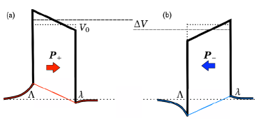
Assuming a Thomas-Fermi model of screening and a constant electric field in the ferroelectric barrier, the static electric potential profile in the electrodes and across the barrier of thickness can be expressed as
| (1) |
with the coordinate along the current direction Zhuravlev et al. (2005); Zhuravlev et al. (2009a); Junquera and Ghosez (2003). With the screening lengths and of the left and the right electrode, respectively, the screening charge per unit area is given by , where is the absolute polarization and the relative static permittivity of the barrier material. The latter was chosen for BTO and PTO 1500 and 250, respectively Ghosez and Junquera (2006). For simplicity, is assumed to be larger than . The average height of the potential barrier depends on the orientation of the polarization, this is, pointing to the left () or to the right () interface. This is due to the fact that the additional electrostatic potential has an averaged value of either or .
II.2 Electronic-structure calculations
For our computational approach a sequential multi-code treatment was applied. Various quantities were carefully cross-checked among the computer codes to obtain consistent results. Reliability is achieved by numerous convergence tests.
Firstly, we determined the fully relaxed atomic positions according to Fechner et al. Fechner et al. (2008) within a pseudopotential and plane-wave-basis scheme using VASP Kresse and Furthmüller (1996). With the ferroelectric polarization pointing along the -direction, the values of for polar bulk BTO and PTO were calculated by a Berry-phase approach Resta and Vanderbilt (2007).
In a second step, the electronic structures of the considered systems, with atomic positions from the first step, were calculated self-consistently within the framework of density-functional theory (DFT), using a scalar-relativistic screened Korringa-Kohn-Rostoker (KKR) Green function method Zahn et al. (1997). The spherical potentials were treated in the atomic sphere approximation (ASA), using the local density approximation (LDA) for the exchange-correlation potential Hohenberg and Kohn (1964); Vosko and Wilk (1980).
In a third step, the complex band structure was computed within a layer KKR, using the same potentials as in the second stage Henk et al. (2006); Henk (2001). The imaginary part of will be denoted as decay parameter . As will become clear in what follows (III.1), evanescent states play an important role in the tunneling regime.
Applying the scheme explained in the upcoming subsection, we are now able to compute the transmission probability which determines the conductance and therefor the TER properties.
II.3 Conductance calculations
In order to predict the conductance change associated with a polarization switching, we assume so thin a barrier that the dominant transport mechanism is quantum-mechanical tunneling and the ferroelectricity is preserved Fong et al. (2004); Spaldin (2004). Therefore, four unitcells ( 1.6 nm) of BTO or PTO are considered as electric switchable barrier.
Assuming elastic and coherent transport, the zero-bias conductance per unit cell area is given by the Landauer-Büttiker formula Büttiker et al. (1985).
| (2) |
where
| (3) |
is the transmission probability in the WKB approximation at the chemical potential . is the smallest imaginary part of the complex wavevector (cf. Section III.1) and is calculated by means of the ab-initio complex band structure. The WKB approximation takes into account the shape of the barrier potential and the decay properties of the electronic states in the barrier gap. The integration is over the whole two-dimensional Brillouin zone, using at least 6000 special points in the irreducible part of the Brillouin zone. The transmission prefactor comprises the influence of the wavefunction matching at the interfaces to the tunneling probability. We used a quite rough approximation, taken to be constant for all energies and inplane wavevectors . This factor drops out in the determination of the TER according to Eq. (4). The change of the potential in the electrodes in the vicinity of the interfaces is not included, because metals with a constant density of states are assumed.
A main feature of transport through FTJs is a conductance asymmetry, defined as
| (4) |
where () is the conductance for the polarization pointing to the right (left) interface.
III Results and discussion
III.1 Complex band structures
To prepare material-specific input for the transport calculations, it is useful to recall the importance of the complex band structure for tunneling through an (ferroelectric) insulator (see Mavropoulos et al., 2000 for magnetic tunnel junctions). The imaginary part of the complex wavevector dominates the transport properties; its product with the barrier thickness defines the exponential decay of the wavefunctions within the barrier and determines essentially the transmission probability.
In a periodic crystal, the wavevectors of Bloch states are necessarily real. Heine Heine (1965) demonstrated that a surface or interface state can be obtained by matching eigenstates of both sides of the boundary plane. This procedure requires in addition states with an imaginary or—more general—a complex wave vector, i. e. so-called evanescent Bloch states. The wave-function matching across the boundary requires eigenstates with complex wave numbers at a given real energy have to be taken into account.
At an interface between a metal and an insulator, prominent states are the metal-induced gap states (MIGS), which are itinerant in the metal electrodes but decay exponentially into the insulating barrier. The dispersion relation of the evanescent states is the so-called complex band structure. For a planar tunnel junction, the periodicity along the interfaces (barrier) requires that the projection of the wave vector onto the interface is real and conserved. However, the perpendicular component can be complex and depends on the region (electrodes, barrier).
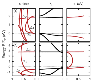
From Figure 2 we deduce fundamental band gaps of ferroelectric BTO and PTO of 1.79 eV and 2.89 eV, respectively. Both are increased, by for BTO and for PTO, as compared to the calculated paraelectric case. The strong localization of the states prevents larger band gaps.
The para-to-ferroelectric phase transition lowers the symmetry from cubic (Pm3m) to tetragonal (P4mm). At , the bands can be decomposed with respect to the irreducible representation of the point group 4mm, as shown in Fig. 2. The bands split to form a doubly degenerate band (, ) and a band (). Similarly, the bands split into a band () and a band ().
According to Chang Chang (1982), complex bands can be classified as follows. (i) Real bands correspond to the conventional band structure and have . Thus, the wave functions are the Bloch states. (ii) Imaginary bands of the first kind have and . (iii) Imaginary bands of the second kind have and . (iv) Complex bands have , and with c being the periodicity in z-direction.
At , the three states with the smallest decay rates within the fundamental band gap consist of a doublet and a singlet for both perovskite ferroelectrics. Neverthless, we address, that the smallest decay rate for BTO is formed by either the or the imaginary band of first kind (cf. 2(a), band crossing in the left panel), while for PTO the smallest decay parameter is always associated with a -like imaginary band of the second kind (cf. 2(b), right panel). Importantly, these complex bands—and hence the electric conductance—are highly sensitive to the ferroelectric displacements; the latter, in turn, depend significantly on the polarization direction and on the potential profile in the barrier.
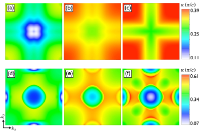
Since at each the transmittance is determined by the least decaying wavefunction, we address the -resolved smallest imaginary part of the wave vector at different energies in Fig. 3. For BTO, the main contribution to the transmission is expected to come from a small annulus around for all energies within the gap. This is caused by the smallest decay rates near the Brillouin zone center. Our findings corroborate those of Velev et al. Velev et al. (2007). In contrast to the paraelectric phase (not shown), the smallest imaginary part of the wavevector is not located exactly at the Brillouin zone center but slightly off-set for energies close to the valence band edge (Fig. 3(a)). This is explained by the lifted degeneracy of the and bands at the -point. The latter supports the importance of a wave-vector analysis in the entire Brillouin zone.
For PTO, the situation is more complex in comparison to BTO. In particular, the smallest are located at and edge centers of the 2BZ for energies close to the valence band maximum and the conduction band minimum (3(d)-(f)). In the middle of the gap, states from the Brillouin zone center dominate the transport (3(e)). In contrast to BTO, one depicts for PTO nearly the same damping around (corners of the Brillouin zone), while sizably larger in the rest of the Brillouin zone can be stated (note the different scale in top and bottom panels of Fig. 3). Thus, one expects remarkably different -transmissions and smaller tunneling currents as compared to BTO.
III.2 Transport Properties
Having provided complex band structures, the tunneling conductance of the FTJs is investigated in dependence on the polarization of the barrier, the screening lengths in the electrodes, and the chemical potential with respect to the fundamental band gap of the barrier. For ferroelectrics, the Fermi energy can be adjusted within the gap by crystal doping Schwartz and Wechsler (2000), while a shift of the chemical potential can be realized by a small bias.
III.2.1 Energy dependence of the TER
We recall that the slope of the imaginary part of the complex wavevector and the distribution in the Brillouin zone change remarkably with energy (cf. Figs. 2 and 3). As a consequence, we focus on three positions in the gap: close to the valence band, in the center of the gap and close to the conduction band.
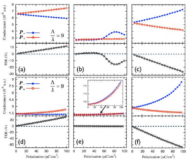
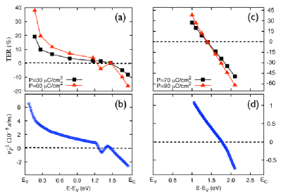
In Figure 4 the calculated conductance and TER for FTJ’s with BTO (upper row, a–-c) and PTO (lower row, d-–f ) as a ferroelectric barrier material are presented. In the upper part of each panel the conductance referring to Eq. (2) is shown. Full blue (open red) circles denote the dependence of the conductance for the polarization pointing to the left (right) interface, while the ratio of screening lengths of the electrodes are fixed at . This might refer to a noble metal electrode () and a ferromagnetic electrode () or a half metallic electrode () as reported in Junquera and Ghosez (2003); Zhuravlev et al. (2005); Gajek et al. (2007). In the lower parts of the panels 4 (a)-(f) the TER determined by Eq. (4) in dependence on the abolute value of the polarization is represented by open black circles.
As we consider different energies in the gap—close to the valence band (a,d), near the gap center (b,e), and close to the conduction band (c,f)—one easily recognizes the increase of the conductance near the gap edges. This is readily explained by the imaginary part of the wavevectors which decreases for certain (compare Figs. 2 and 3). Hence, the transmission probability and the conductance (ref. to Eq. (3)) increase. In a free electron picture as used in previous explanations of the TER effect Zhuravlev et al. (2005); Zhuravlev et al. (2009a); Yang et al. (2007); Zhuravlev et al. (2009b), the conductance would decrease continuously by shifting the chemical potential from the band edges. Our approach takes into account a more realistic electronic structure of the ferroelectric barrier.
The behavior of the conductance for different chemical potentials can be understood qualitatively by the complex band structure at (see Fig. 2). For energies near the valence band the -conductance is larger than the conductance (compare Fig. 4(a,c)). This is caused by the lower decay rates for the electron wave functions contributing to the tunneling current in the state. The shift of the bands to higher energies due to the positive contribution of the electrostatic potential leads to smaller values of the imaginary part of the wave vector at the chemical potential. Taking into account the definition of the TER (ref. Eq. (4) a positive TER occurs. For energies close to the conduction band edge the behavior of the conductances and, thus, of the TER reverse, as does the curvature of the imaginary bands reverse, too.
For bulk polarizations of and Fechner et al. (2008) we achieve high TER values of nearly 3 % () and 27 % () for chemical potentials near to the valence band and allmost 6 % () and 61 % () for energies close to the conduction band. The value for PTO is in agreement with experimental values of nearly 60 % for a FTJ with Pb(Zr,Ti)O as ferroelectric barrier with different electrode materials Contreras et al. (2003). Recent findings for FTJs based on strained BTO show a TER of 16 % Garcia et al. (2010), which is in astonishing agreement with our predictions (see Fig. 4(c)) for strained thin films (note that then according to Ederer and Spaldin (2005)).
As for energies lying close to the gap edges the discussion can be made in a generally more intelligible picture, the situation is quite more complex for energies in the middle of the gap. In figure 4(b) the evaluation of the TER for a FTJ consisting of BTO is shown for near the point where the symmetry character of the dominating evanescent wave functions at the -point changes from to (compare Fig. 2(a), left panel) and consequently the slope of the imaginary bands change sign.
For polarization strengths less than the TER nearly vanishes, while for higher polarization strengths the conductance for the state increases and a negative TER of can be reached. As noted earlier, those higher polarization strengths might be achieved in stressed thin films where values of and even were reported Ederer and Spaldin (2005). In the case of PTO the TER is barely visible for the whole range of polarizations with values below 1 % for an energy of . This is near the center of the complex wave vectors loop as shown in Fig. 2(b), right panel. Close to the maximum of the band with respect to the decay rates, a small shift of the potential caused by the electric polarization reversal causes a negligible change of the decay rates, only.
As the decay parameters of all states in the Brillouin zone are comprised for the calculation of the transport properties, different curvatures of are involved in the total resulting TER and a straightforward explanation of the properties of the TER is hardly possible. In the preceding, we established major trends by discussing three exemplary energies. Now, we turn to the TER in dependence on the position of the chemical potential relative to the barrier gap. In the upper row of Fig. 5, the most remarkable feature is a change of sign of the TER at energies of about 1.5 eV for both materials. This result cannot be explained by a free electron model, where the negative slope of the imaginary band would lead to negative values of the TER over the whole range of the band gap. Furthermore, nearly free electron models or tight-binding approaches would produce only one sign change at an energy approximately in the middle of the gap, which is at about 0.8 eV and 1.4 eV for BTO and PTO, respectively.
For the chosen polarization values and for energies close to the valence band of BTO, the TER is expected to be as twice as large as for energies close to the conduction band. For PTO even higher values of 40 % (close to the valence band) and -60 % (close to the conduction band) are expected.
III.2.2 Inverse imaginary Fermi Velocity
A qualitative explanation for the previous described energy dependent behavior of the TER is provided by the introduction of the inverse imaginary Fermi velocity
| (5) |
This quantity can be seen as the -averaged energy derivative of the decay parameter of the complex band structure in the Brillouin zone. If this parameter is small, the additional electrostatic potential caused by the electrical polarization or does not change the effective decay parameter remarkably. So, a small TER effect is expected. On the contrary, a large energy derivative of the decay parameter which most likely occurs close to the band edges points to a large TER effect.
To illustrate the correlation of the inverse imaginary Fermi velocity and the TER, an approximation for a single is given in the following. Small polarizations will lead to small differences in the complex bandstructure for both . Hence, the imaginary part of the complex wavevector for can be written as
| (6) |
by expanding the imaginary part for . The TER given in Eq. (4), including Eqs. (3) and (6) is directly heading to the approximation
| (7) |
Here,
| (8) |
is a unique constant for each junction, as and contain material-specific information of the ferroelectric barrier and the screening lengths and are determined by the electrodes. An explicit value of for BTO (, , , ) would be .
The effect of all states in the whole Brillouin zone has to be recognized to describe the TER effect in a reliable way. Therefor the inverse imaginary Fermi velocity is a combined quantity for the damping of all wavefunctions in the Brillouin zone and hence a value for the probability of transmission. The lower panels in Fig.5 depict the inverse imaginary Fermi velocity for ferroelectric BTO (b) and PTO (d). The behavior of the TER is fully reproduced qualitatively and quantitatively. To be more specific, the energy position of the sign change in the TER as well as the magnitude of the TER for different chemical potentials can be achieved by analyzing the inverse imaginary Fermi velocity. The different ratios between the TER and the inverse imaginary Fermi velocity are caused by the relative static permittivities for BTO and PTO. This also prevents the calculation of the TER for PTO junctions for chemical potentials close to the band edges, as electrical breakthrough and metallic behavior would be the consequences.
The perfect agreement of the behavior of TER and the inverse imaginary Fermi velocity is to some extent accidental. The average over is taken in the whole 2BZ, whereas the transmission defined in Eq. (3) is dominated by the states with the lowest decay parameters . It seems that these regions of the 2BZ are also dominated by the averaged inverse Fermi velocity. For the barrier materials BTO and PTO the latter could be found. Introducing the exact material properties of the electrodes, the symmetry selection caused by the wavefunction matching conditions at the interfaces would most likely weaken the link between the TER and .
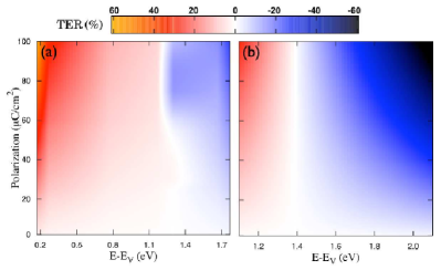
To complete the discussion, we show in Fig. 6 the dependence of the TER on and . For BTO, the energetic position of the sign change of the TER varies slightly with the polarization strength, which is most likely linked to the change of symmetry character of the dominating evanescent wave functions associated with a sign reversal of the inverse imaginary Fermi velocity at the crossing point of the two imaginary bands of the first kind at an energy of about 1.4 eV above the valence band edge (compare top panel in Fig.2). In the case of PTO the sign change is obtained for a chemical potential of about 1.4 eV above the valence band edge, independent on the intrinsic polarization strength. Again it is conspicuous that the highest values for the TER occur near the band edges, where the inverse imaginary Fermi velocity is maximized. The largest absolute values for the TER are found near the valence band maximum or conduction band minimum for BTO or PTO, respectively.
III.2.3 Influence of the electrodes’ screening lenghts
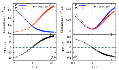
To get more insight on how the TER depends on the electrodes’ properties, we present in Fig. 7 its dependency on the ratio of the screening lengths for . The spreading of the conductances for and increases with the difference of the screening lengths. An interchange of the electrodes will not affect the conductances, as only the polarization direction is reversed. An asymmetry of the screening lengths in the electrodes is mandatory to obtain a nonzero TER. For equal screening lengths, one obtains and, hence, the TER vanishes. On the other hand, an interchange of the screening lengths in the electrodes reverses the sign of the TER as a result of the definition in Eq. (4). If one interface is a free surface, the ratio of the screening lengths will be maximized, leading to giant values of the TER as observed with conductive atomic force microscopy on BTO and PTO surfaces Garcia et al. (2009); Gruverman et al. (2009); Crassous et al. (2010).
IV Conclusion and outlook
The tunneling electroresistance in ferroelectric tunnel junctions with BTO and PTO barriers was discussed in dependence on the position of the chemical potential, the electrical polarization, and the ratio of the screening lengths in the electrodes. In dependence on the chemical potential position a sign reversal of the TER ratio is obtained. This is caused by a sign change of the energy derivative of the decay parameter . The latter was comprised by the inverse imaginary Fermi velocity. The behavior of this quantity in the band gap is in agreement with the TER ratios.
As a consequence of the presented results we demonstrate that the analysis of the complex band structure is a powerful tool to gain useful insight into the behavior of the TER effect more precise than the analysis of free electron like models and more efficient than calculations of the full contact geometry done in previous works.
As a sign change of the TER in dependence on the chemical potential is achieved, an experimental proof by application of different electrode materials or doping levels is proposed. We again emphasize that the shift of the chemical potential and thus the desired sign change of the TER might be also achieved by a small applied bias.
Acknowledgements.
This work was supported by the Deutsche Forschungsgemeinschaft, SFB 762 ‘Functionality of Oxide Interfaces’. N. F. Hinsche, M. Fechner, and P. Bose are members of the International Max Planck Research School for Science and Technology of Nanostructures.References
- Scott and Araujo (1989) J. Scott and C. P. D. Araujo, Science 246, 1400 (1989).
- Tsymbal and Kohlstedt (2006) E. Y. Tsymbal and H. Kohlstedt, Science 313, 181 (2006).
- Laibowitz et al. (1971) R. Laibowitz, L. Esaki, and P. Stiles, Physics Letters A 36A, 429 (1971).
- Zhuravlev et al. (2005) M. Zhuravlev, R. Sabirianov, S. Jaswal, and E. Y. Tsymbal, Phys. Rev. Lett. 94, 246802 (2005).
- Zhuravlev et al. (2009a) M. Y. Zhuravlev, R. F. Sabirianov, S. S. Jaswal, and E. Y. Tsymbal, Phys. Rev. Lett. 102, 169901 (2009a).
- Shaw et al. (2000) T. M. Shaw, S. Trolier-McKinstry, and P. C. McIntyre, Annual Review of Materials Science 30, 263 (2000).
- Junquera and Ghosez (2003) J. Junquera and P. Ghosez, Nature 422, 506 (2003).
- Spaldin (2004) N. A. Spaldin, Science 304, 1606 (2004).
- Sai et al. (2005) N. Sai, A. M. Kolpak, and A. M. Rappe, Phys. Rev. B 72, 020101 (2005).
- Fong et al. (2004) D. D. Fong, G. B. Stephenson, S. K. Streiffer, J. A. Eastman, O. Auciello, P. H. Fuoss, and C. Thompson, Science 304, 1650 (2004).
- Despont et al. (2006) L. Despont, C. Koitzsch, F. Clerc, M. Garnier, and P. Aebi, Phys. Rev. B 73, 094110 (2006).
- Contreras et al. (2003) J. R. Contreras, H. Kohlstedt, U. Poppe, R. Waser, C. Buchal, and N. A. Pertsev, Applied Physics Letters 83, 4595 (2003).
- Gajek et al. (2007) M. Gajek, M. Bibes, S. Fusil, K. Bouzehouane, J. Fontcuberta, A. Barthélémy, and A. Fert, Nature Materials 6, 296 (2007).
- Garcia et al. (2009) V. Garcia, S. Fusil, K. Bouzehouane, V. Garcia, S. Enouz-Vedrenne, N. D. Mathur, A. Barthelemy, and M. Bibes, Nature 460, 81 (2009).
- Garcia et al. (2010) V. Garcia, M. Bibes, L. Bocher, S. Valencia, and F. Kronast, Science 327, 1106 (2010).
- Crassous et al. (2010) A. Crassous, V. Garcia, K. Bouzehouane, S. Fusil, A. H. G. Vlooswijk, G. Rispens, B. Noheda, M. Bibes, and A. Barthélémy, Applied Physics Letters 96, 042901 (2010).
- Gruverman et al. (2009) A. Gruverman, D. Wu, H. Lu, Y. Wang, H. Jang, C. Folkman, M. Zhuravlev, D. Felker, M. Rzchowski, C. Eom, et al., Nano Letters 9, 3539 (2009).
- Yang et al. (2007) F. Yang, M. H. Tang, Z. Ye, Y. C. Zhou, X. J. Zheng, J. X. Tang, J. J. Zhang, and J. He, J. Appl. Phys 102, 044504 (2007).
- Zhuravlev et al. (2009b) M. Zhuravlev, Y. Wang, and S. Maekawa, Applied Physics Letters 95, 052902 (2009b).
- Velev et al. (2008) J. Velev, C. Duan, J. Burton, and A. Smogunov, Nano Letters 9, 427 (2008).
- Zahn et al. (1997) P. Zahn, I. Mertig, R. Zeller, and P. Dederichs, Mat. Res. Soc. Symp. Proc. 475, 525 (1997).
- Henk et al. (2006) J. Henk, A. Ernst, K. Saha, and P. Bruno, J. Phys.: Condens. Matter (2006).
- Büttiker et al. (1985) M. Büttiker, Y. Imry, R. Landauer, and S. Pinhas, Phys. Rev. B (1985).
- Mehta et al. (1973) R. R. Mehta, B. D. Silverman, and J. T. Jacobs, J. Appl. Phys 44, 3379 (1973).
- Gerra et al. (2007) G. Gerra, A. K. Tagantsev, and N. Setter, Phys. Rev. Lett. 98, 207601 (2007).
- Ghosez and Junquera (2006) P. Ghosez and J. Junquera, First-Principles Modeling of Ferroelectric Oxide Nanostructures (American Scientific Publishers, 2006), vol. 7 of Handbook of Theoretical and Computational Nanotechnology, chap. 134, p. 105.
- Fechner et al. (2008) M. Fechner, S. Ostanin, and I. Mertig, Phys. Rev. B 77, 094112 (2008).
- Kresse and Furthmüller (1996) G. Kresse and J. Furthmüller, Physical Review B 54, 11169 (1996).
- Resta and Vanderbilt (2007) R. Resta and D. Vanderbilt, Physics of Ferroelectrics: A Modern Perspective (Springer-Verlag, Berlin, Heidelberg, 2007), chap. 2.
- Hohenberg and Kohn (1964) P. Hohenberg and W. Kohn, Phys. Rev. 136, B864 (1964).
- Vosko and Wilk (1980) S. H. Vosko and L. Wilk, Phys. Rev. B 22, 3812 (1980).
- Henk (2001) J. Henk, Handbook of Thin Film Materials, Vol. 2 (Academic Press, San Diego, 2001), chap. 10.
- Mavropoulos et al. (2000) P. Mavropoulos, N. Papanikolaou, and P. H. Dederichs, Phys. Rev. Lett. 85, 1088 (2000).
- Heine (1965) V. Heine, Phys. Rev. 138, A1689 (1965).
- Chang (1982) Y. Chang, Phys. Rev. B 25, 605 (1982).
- Velev et al. (2007) J. P. Velev, C. Duan, K. D. Belashchenko, S. Jaswal, and E. Y. Tsymbal, Phys. Rev. Lett. 98, 137201 (2007).
- Schwartz and Wechsler (2000) R. N. Schwartz and B. A. Wechsler, Phys. Rev. B 61, 8141 (2000).
- Ederer and Spaldin (2005) C. Ederer and N. A. Spaldin, Phys. Rev. Lett. 95, 257601 (2005).