Embedded Ribbons of Graphene Allotropes: An Extended Defect Perspective
Abstract
Four fundamental dimer manipulations can be used to produce a variety of localized and extended defect structures in graphene. Two-dimensional templates result in graphene allotropes, here viewed as extended defects, which can exhibit either metallic or semiconducting electrical character. Embedded allotropic ribbons–i.e. thin swaths of the new allotropes–can also be created within graphene. We examine these ribbons and find that they maintain the electrical character of their parent allotrope even when only a few atoms in width. Such extended defects may facilitate the construction of monolithic electronic circuitry.
1 Introduction
The presence of defects in condensed matter has a dramatic influence on electrical character. Extended defects such as dislocations, grain boundaries, and phase interfaces, for instance, tend to have a deleterious effect on electron mobility and can serve as unwanted recombination sites in photovoltaic materials. The introduction of localized dopant defects to tune electronic structure, on the other hand, is a mainstay of the semiconductor industry. Whether unavoidably present or intentionally introduced, localized and extended defects tend to be statistically distributed. The precise placement of defects, though, crosses the line into materials architecture.
Graphene offers a particularly attractive setting for such defect engineering. Its two-dimensional geometry implies that the entire domain is accessible to external manipulation. Although such manipulations may seek to modify thermal, mechanical, or chemical character, our current focus is to provide a means for the creation of monolithic carbon logic circuitry. This requires that it be possible to create conductors, semiconductors, and charge confinement structures. In addition, composite systems must be structurally stable and should not unduly modify individual character. Charge may then be introduced, confined, gated and routed within a single sheet.
Our approach is in contrast to a number of other strategies which are being explored to manipulate the electronic structure of graphene. Those tend to focus on the use of external agencies to distort graphene so that it exhibits a band gap. Such external agencies include the use of strongly interacting substrates [1, 2, 3] or the application of electric fields in graphene bi-layers [1, 4, 5]. Quantum confinement effects can also be exploited as in carbon nano-ribbons (CNRs) [6, 7] or carbon nano-meshes [8]. Another approach to tailoring graphene is chemical modification. For instance, hydrogen can be introduced so as to change the bonding from sp-2 to sp-3 to create the corrugated insulator graphane [9]. Similarly, a graphene oxide insulator can be created via bonding with hydroxyl groups [10]. The external agency can also appear in the form of neighboring regions of foreign material as in composite two-dimensional structures that harbor domains of graphene [11]. We consider an intrinsic approach to modification, though, wherein defects are introduced into the graphene in order to endow it with new electronic properties. Several other researchers in the field are also exploring such defect modifications [12].
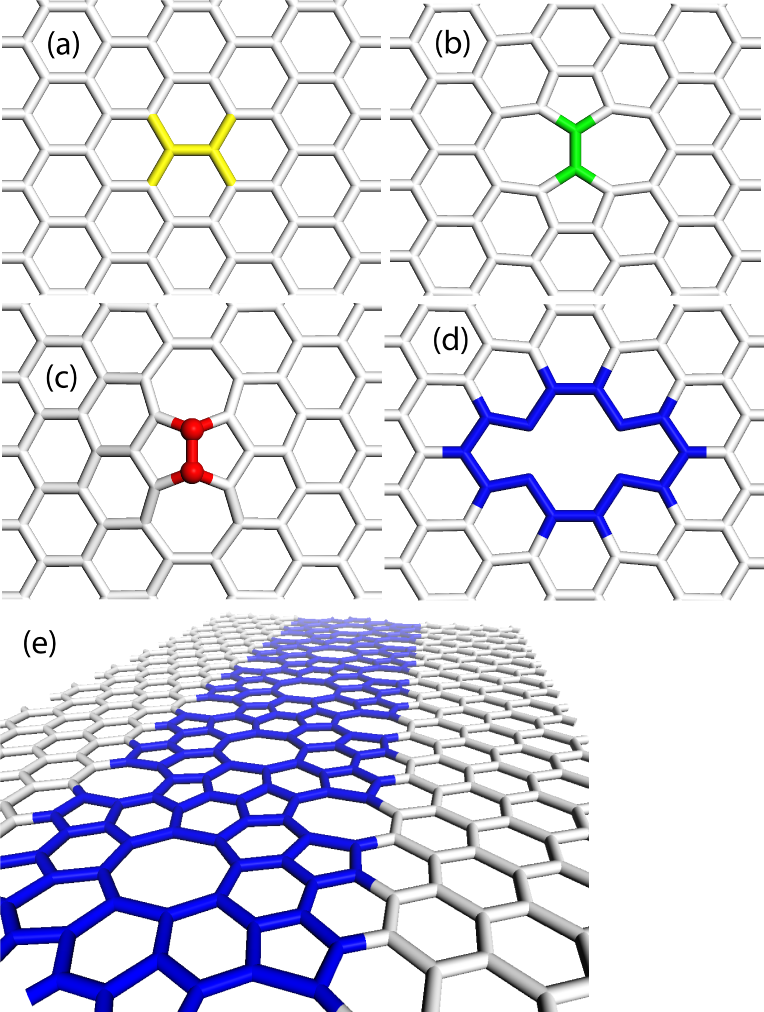
In a series of earlier works, we have identified simple defects from which a variety of localized and extended structures can be fabricated [13, 14, 15, 16]. Our perspective is now that the design space is best described as four basic operations that can be performed on a single carbon dimer. These are shown in Fig. 1. The first is the identity operation in which an existing carbon dimer is left unchanged. The second is the familiar Stone-Thrower-Wales (STW) defect consisting of a rotation of a carbon dimer. Addition of a dimer constitutes the third configuration and results in an Inverse Stone-Thrower-Wales (ISTW) defect [17, 13]. Conversely, removal of a carbon dimer results in a di-vacancy (DV) defect, the fourth letter in our alphabet. All structures to be considered can be reduced to a weighted sum of these basic building block. Even when distinct from the actual synthesis routes, the analytical fabrication of structures as a sequence of dimer additions, subtractions, rotations and preservations lends a new type of insight into form and function.
All elements of this defect alphabet have been experimentally observed [18, 19, 20, 21]. STW defects have been extensively studied in both graphene [22, 23] and CNTs [24, 25], and they can be created by scanning tunneling microscopy (STM) [26] or atomic force microscopy (AFM) [27]. DV defects can be precisely created via irradiation [19]. Recently, an electron irradiation beam focused to was shown to be capable of precisely creating vacancies in CNTs [18]. DVs have also been considered theoretically within a CNT setting, where molecular dynamics annealing causes them to reconstruct into 5-8-5 defects [28, 29]. A series of ad-dimer ISTW defects have been experimentally achieved [21] by focusing on the interatomic spacing of the defect rather than on physically depositing a dimer on the graphene. Direct dimer addition may be another avenue of achieving the ISTW defect as advances in experimental methods of graphene manipulation are now approaching atomic fidelity using Scanning Tunneling Microscopy (STM) [26], Atomic Force Microscopy (AFM) [27] and via novel inventions such as the one proposed by Allis and Drexler [30].
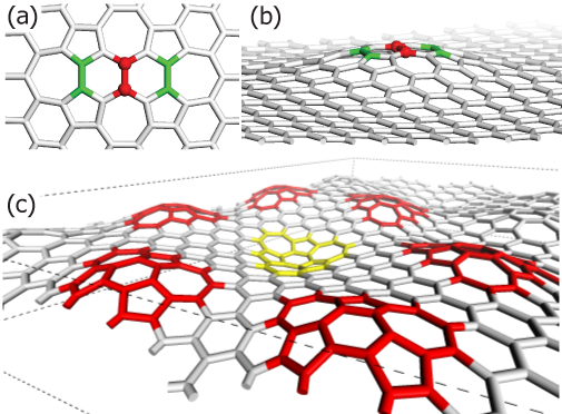
In this work, we focus on patterned defect structures obtained by replication of a defect unit, a combination of the basic alphabet members. For instance, ad-dimers can be used to create nonplanar blisters by adding STW defects to either side as shown in Fig. 2(a, b). Larger blisters can also be created using additional ISTW defects, and graphene islands can even be made to bubble up when corralled by a loop of the ad-dimers [13]. Replication of localized blisters results in the metacrystal shown in Fig. 2(c). However, even closer packing can result in planar allotropes of graphene [14]. These allotropes may be either conducting or semiconducting merit a brief review because they are a starting point for the embedded defect ribbons that we have in mind, i.e., thin strips of an allotrope existing within a parent graphene sheet. These ribbons are the monolithic analog of graphene nanoribbons [6], but their electronic character is intrinsic and not due to the presence of free boundaries. We will show that both conducting and semiconducting ribbons can be constructed within a completely planar setting.
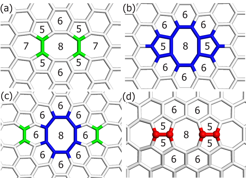
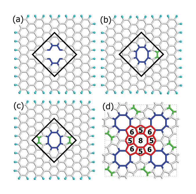
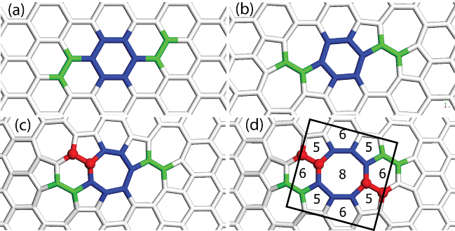
The electrical, and most likely magnetic, properties of graphene allotropes are not attributable to any one of the fundamental dimer operations but rather the type, arrangement, and misfit distortion of the carbon rings that results. For instance, octagonal rings can be created with differing combinations of dimer operations so as to give differing types of neighbor rings. Adjacent STW defects can create an octagon surrounded by pentagons, hexagons and heptagons, and this is illustrated in Fig. 3(a). An octagon can also be created when a DV pinches in at left and right, as shown in Fig. 3(b). Here the resulting octagon is encircled with only pentagons and hexagons. The addition of STW defects on either side, though, results in a periphery of only hexagons, Fig. 3(c). On the other hand, two adjacent STW defects create an octagon surrounded by alternating pentagons and heptagons, and two ISTW defects create on octagon between them with a new arrangement of pentagons and heptagons, Fig. 3(d) [15]. This variety of octagonal defect combinations have recently resulted in the prediction of a number of new graphene allotropes [31, 32].
Our computational approach is outlined in Sec. 2, where we also provide comparative checks against previously obtained computational and experimental data. In Sec. 3 we consider the construction and electronic structure of metallic and semiconducting graphene allotropes. Section 4 focuses on the creation and analysis of thin, embedded ribbons of these allotropes within graphene to establish their structural stability and electronic character. Finally, in Sec. 5 we conclude.
2 Methodology and the Formation Energies of the Fundamental Defect Structures
Density functional theory (DFT) is employed throughout this work to estimate ground state structure and predict electronic character. A real-space numerical atomic orbital code [33] was used to initially relax the structures until the energy change was less than eV. A double numeric precision basis set was employed and the Perdew-Wang generalized gradient approximation used to account for electron exchange and correlation energy [34]. This computational setting has been shown to accurately predict defect geometries and energies associated with graphene structures [13, 14, 15].
In order to more thoroughly examine the band structure of a semiconducting allotrope, a second DFT implementation was also used which employs a plane-wave basis set [35, 36, 37, 38]. There a Projector Augmented Wave [39, 40] approach with energy cutoff of 400 eV was used within a Generalized Gradient Approximation [41] and 24x24x1, -centered k-space grid to compute the band structure and density of states. The methodology was also extended to account for quasiparticle effects, within a approximation, [42] because DFT typically underestimates the band gap of periodic structures [43].
A STW defect was estimated to have a formation energy of 5.08 eV when embedded within a 144-atom graphene supercell; this compares well with an estimate of 4.8 eV from the literature [22]. The formation energy required to create an ISTW defect, calculated using a 200-atom supercell, was found to be 6.20 eV [13]. The energy required to create a DV in a 200 atom periodic supercell was 7.6 eV in agreement with previous DFT estimates of 8.7 eV [44] and 7.5 eV [24]. These formation energies are tabulated in Table 1.
| Defect | eV | Number of atoms in supercell |
|---|---|---|
| STW | 144 | |
| ISTW | 200 | |
| DV | 200 |
3 Graphene Allotropes from Templated Defects
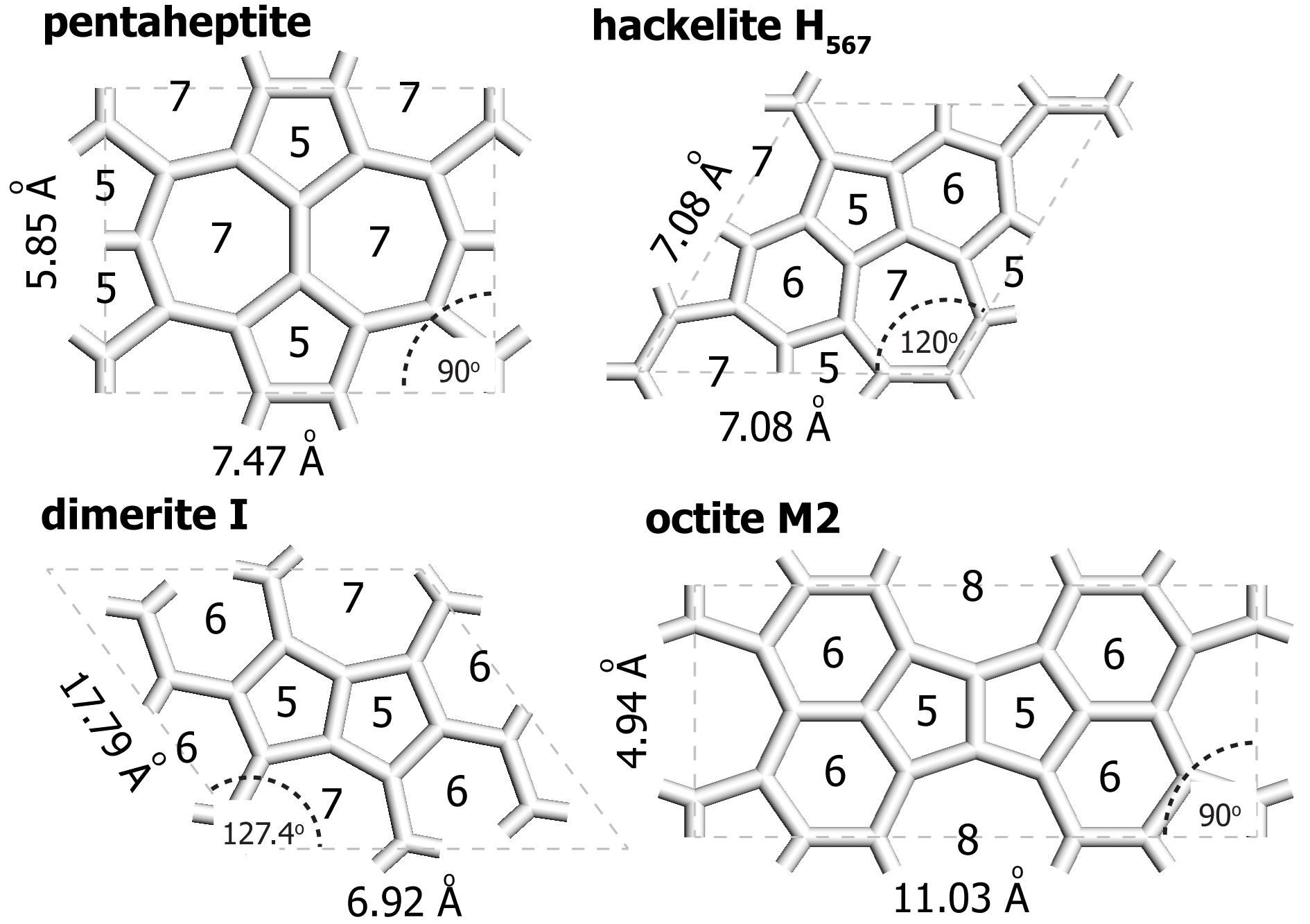
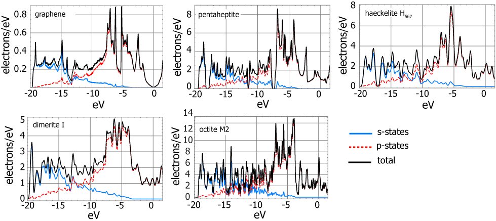
Even before the experimental realization of graphene in 2004 [45], planar allotropes had been predicted with properties distinct from graphitic sheets. Motivated by a desire to find a pure carbon allotrope with a high Density of States (DOS) at the Fermi level, Crespi suggested that graphene allotropes with zero net curvature could form periodic, two-dimensional crystals [46] and proposed the pentaheptite structure shown in Fig. 4. A family of planar allotropes of carbon created from combinations of five-, six-, and seven-sided rings was proposed shortly thereafter [47]. Dubbed haeckelites, these sheets were predicted, using tight-binding calculations, to have a metallic character. The two lowest energy structures are shown in Fig. 4.
More recently, a tie between allotropes and defects was established by showing that pentaheptite and all haekelites can be constructed using STW and ISTW defects [14]. This led to the prediction of a new family of graphene allotropes named dimerites because of their exclusive dependence on only the ad-dimer ISTW defect. The lowest energy dimerite is shown in Fig. 4. While generally in higher energy than the haeckelite allotropes, dimerites are promising structures for synthesis because they can be made entirely from ad-dimers.
A subsequent focus on defect arrangements resulting in octagons led to the prediction of a new family of allotropes called octites [31, 32], the name reflecting the presence of eight-membered rings. The octite family includes three metallic allotropes of lower in energy than any haeckelite and an intrinsic semiconducting graphene allotrope. We use an M or SC to indicate metallic or semiconducting character.
| Allotrope | meV/atom Above Graphene | Atoms in Unit Cell | Defect Composition |
|---|---|---|---|
| graphene | 2 | 0 | |
| octite M1 | 20 | 2 STW + 2 ISTW | |
| octite M2 | 20 | 2 ISTW | |
| octite M3 | 34 | 2 STW + 2 ISTW | |
| haeckelite | 16 | 1 STW + 1 ISTW | |
| dimerite I | 16 | 1 ISTW | |
| octite SC | 28 | 2 STW + 1 DV | |
| dimerite II | 40 | 2 ISTW | |
| octite M4 | 8 | 1 STW | |
| haeckelite | 12 | 1 STW | |
| dimerite III | 30 | 3 ISTW | |
| haeckelite | 16 | 2 STW | |
| buckeyball C60 | 60 | - |
The pentaheptite, haeckelites and dimerites are predicted to be conductors as shown in the Density of States (DOS) summaries of Fig. 5. All of these can be constructed by patterning of STW and ISTW defects. Similarly, metallic octites are composed of STW and ISTW defects. This apparent correlation motivated us to search for a new type of defect building block that would lead to a semiconducting carbon sheet. The result was the addition of the DV defect as a third basic building block [32].
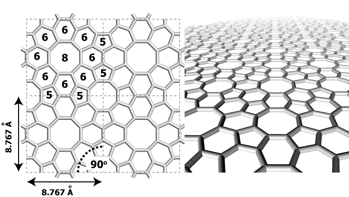
Of particular interest is a new semiconducting allotrope, octite SC, which can be constructed from a combination of STW and DV defects. It amounts to a patterning of the defect assemblies shown in Fig. 3 (a) and (b). To see this, consider the 170-atom carbon sheet of Fig. 6(a). The edges are passivated with hydrogen to maintain sp-2 bonding for all carbon atoms and a single DV defect is introduced. Two bond rotation defects are subsequently imposed (b and c). The result is then replicated so as to create an array of octagonal defects. Octagons surrounded by hexagons result from DV and STW defects while smaller octagons surrounded by alternating pentagons and hexagons derive from STW defects (d). The planar arrangement of atoms with three nearest neighbors suggests sp-2 bonding, although variations in bond length (1.40 to 1.54 ) indicate that the three-fold symmetry of graphene bonding is no longer present. For the sake of comparison, sp-2 bond lengths in graphene are 1.42 while the sp-3 bond length of diamond are 1.54 .
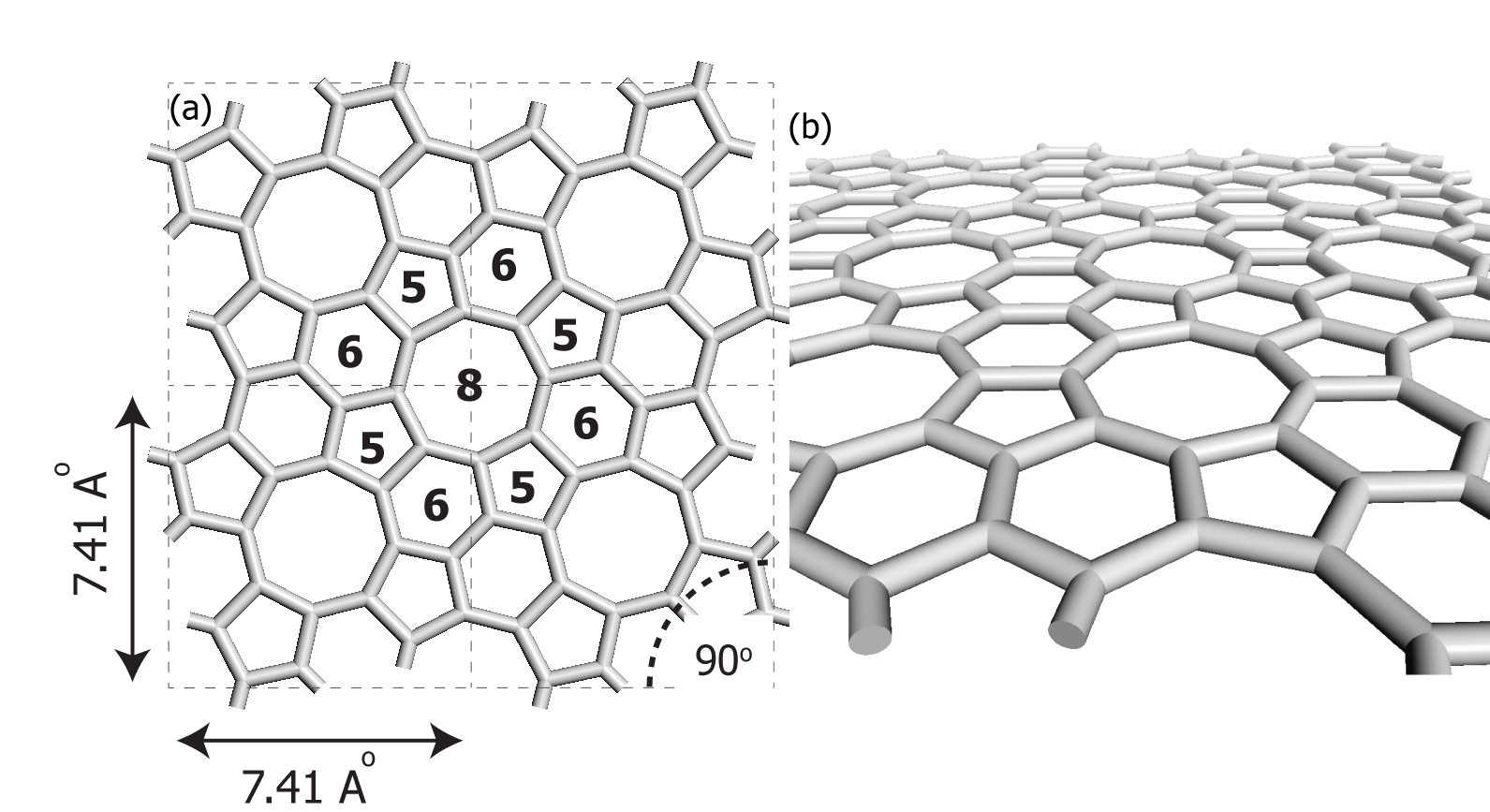
The stand-alone form of this semiconductor is shown in Fig. 7. It has a primitive cell of 28 atoms arranged in pentagons, hexagons, and octagons. The planar density is 0.364 atoms per , comparable to 0.380 atoms per for graphene. The central geometrical feature is an octagon completely surrounded by hexagons. The cell geometry is square with p4/MMM symmetry. A Hessian linear vibrational analysis showed the structure to be a local energy minimum. Room temperature quantum molecular dynamics simulations were also used to confirm its stability.
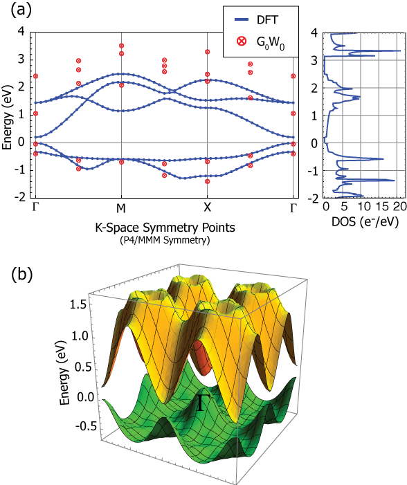
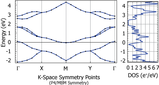
The ground state structure was verified using a second DFT implementation that employs a plane-wave basis set [35, 36, 37, 38]. The wave function energy cutoff was set at 400 eV, and a conjugate gradient method employing a 4x4x2 Monkhorst-Pack grid resulted in the same ground state structure but with a lattice constant of 8.674 . The plane-wave DFT code was used to predict both the band structure (BS) and Density of States (DOS). A 24x24x1, -centered k-space grid was used to calculate the electronic properties. The BS and DOS diagrams are shown in Fig. 8. The material possesses a 0.2 eV direct band gap at the point. As in graphene, all carbon atoms bond with three nearest neighbors, but the symmetry of the in-plane sp-2 character has been disrupted by the varying bond angles and bond lengths.
DFT typically underestimates the band gap of periodic structures [43], so the 0.2 eV gap should be viewed as a lower bound. Many-body perturbation theory, within the approximation [42], was therefore used to provide a more accurate estimate of the electronic structure. As expected, the inclusion of quasiparticle effects widens the band gap, providing an estimate for the direct, point gap of 1.1 eV. The band structure is shown with its DFT counterpart in Fig. 8. Three iterations towards self-consistency ( approximation) opened the band gap slightly to 1.2 eV.
Metallic allotropes can also be composed of octagonal rings, and three have been computationally predicted to have the lower ground state energies than any previous allotrope [31]. One of them, octite M1, has an energy only 194 meV/atom above graphene–lower than the 233 meV/atom calculated for the lowest energy haeckelite or the 284 meV/atom for the lowest energy dimerite. This structure is important because it is expected to be the most stable of any predicted graphene derivative which therefore makes it a likely candidate for experimental realization. In all of the metallic octites, octagonal rings are built exclusively from ISTW and STW defects. This is in contrast to the semiconducting octite wherein DVs are employed to build octagons with a different local environment.
From the perspective of defect engineering, the octite M1 can be constructed from a template composed of two STW defects and two ISTW defects as shown in Fig. 9. This synthesis route was carried out computationally on a rectangular supercell of graphene measuring 21.34 by 12.32 . The intermediate steps were geometrically optimized DFT ground states after each defect was introduced, but the lattice was not allowed to dilate. The initial zero energy state is graphene with two dimers at infinity. Two STW bond rotations (b) raise the energy to 9.1 eV but dimer addition through ISTW defects lowers the energy to 1.6 eV (c) and finally to -6.8 eV.
The resulting octite M1, shown in Fig. 10, is completely flat and contains 20 atoms in the primitive unit cell. The energy minimum was verified via a Hessian vibrational matrix. Quantum molecular dynamics simulations were also utilized, at 300 K and 500 K, to ensure that the structure is indeed stable.
Density of States (DOS) calculations were performed using a Monkhorst-Pack [48] grid size of 12x12x4 which was then interpolated onto a grid of 200x200x200 points. A slight broadening of 0.05 eV was applied for a more physical representation of the DOS in a large system. Fig. 11 shows that octite M1 is a good conductor with approximately 2 electrons/eV at the Fermi level.
4 Embedded Ribbons of Graphene Allotropes
The link between defects and allotropes provides the design guidance needed to create both localized and extended regions of semiconducting and/or conducting material within graphene. We take up this issue by investigating embedded allotropic ribbons, i.e., a thin strip of one allotrope embedded within another. These are distinguished from nanoribbons which are thin strips of material with free boundaries. Nanoribbons have been promoted as a means of endowing graphene with a tunable band gap, and the approach requires that a thin strip of graphene be precisely cut to a prescribed chirality and width. Lateral confinement of the charge carriers creates a band gap [49]. Computational studies have determined that nanoribbons can be conductive or insulating depending on the shape of their edges [6]. Embedded allotropic ribbons offer an alternative strategy wherein both conducting and semiconducting pathways can be created on a single, planar sheet of carbon. We examine both types of ribbons embedded within a graphene sheet.
A minimal ribbon of a conducting octite (Figs. 4 and 5) within graphene is shown in Fig. 12(a). Within this setting, the extended defect amounts to an alternating sequence of octagons and paired pentagons. The relaxed, planar ground state structure is a conductor (Fig. 12(b)) with band edge states consistent with that previously determined for isolated ISTW defects [15]. Specifically, the tops of the ad-dimers repel additional electrons while the shoulders of the extended defect actually attract additional electrons. This is made clear in Fig. 12(c, d) which show the highest occupied and lowest unoccupied molecular orbitals (HOMO/LUMO). These orbitals are constructed using a -point () spatial frequency, i.e., by setting the Bloch function wave number to zero and relying on linear combinations of atomic orbitals to describe the electronic structure. These band edge states are both localized along the ribbon, and the ribbon itself endows the composite with a high DOS at the Fermi level, similar to vacancy localization effects found in bilayer graphene[50]. The composite structure is a conductor as shown in Fig. 12(b).
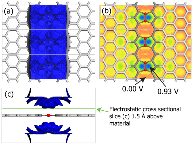
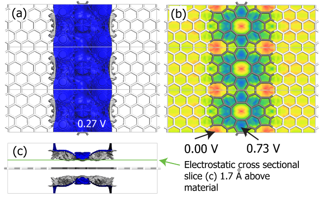
The conducting nature of the composite is presumably due to electron transport along the extended defect. This is supported by plots of the electrostatic potential provided in Fig. 13. The isosurface shown in panel (a) indicates that the defect has a positive potential and thus attracts additional charge, while panel (b) shows potential contours in a plane that intersects the isosurface.
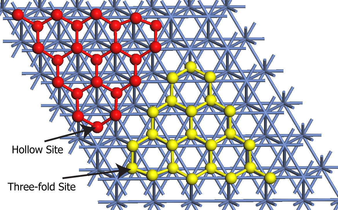
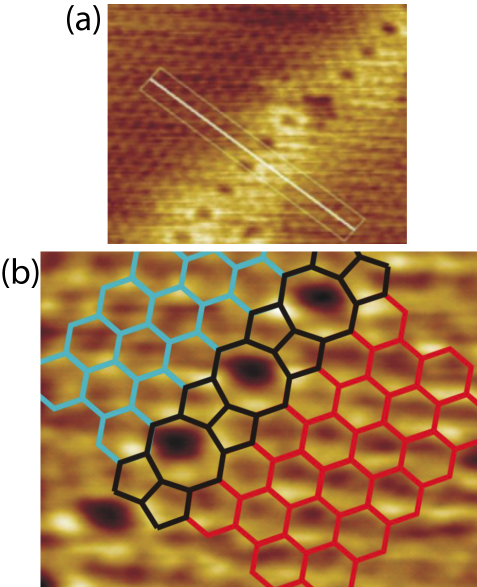
Significantly, this metallic defect ribbon has recently been experimentally synthesized [21, 16, 31]. Graphene was grown epitaxially on the (111) surface of nickel, where graphene may be aligned in one of two nearly energetically equivalent ways: one-half of the carbon atoms may lie over either three-fold or hollow sites as shown in Fig. 14. The mismatch in carbon atoms at the interface of dissimilar graphene flakes results in the extended defect structure of Fig. 12. The nickel can be subsequently removed resulting in a stand-alone sheet of graphene with a minimal ribbon of dimerite. Although not measured experimentally, DFT analysis performed by Batzill et al. [21] in the localized density approximation suggested that these ribbons are metallic, consistent with our own DFT studies using a generalized gradient approximation. The experimental result is provided in Fig. 15 [21]. This suggests that the realization of more complex defect designs is only a matter of time.
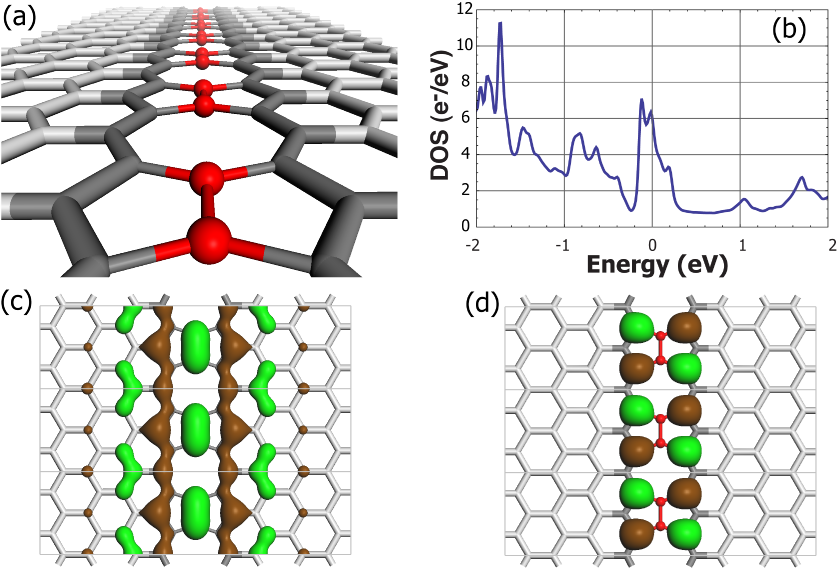
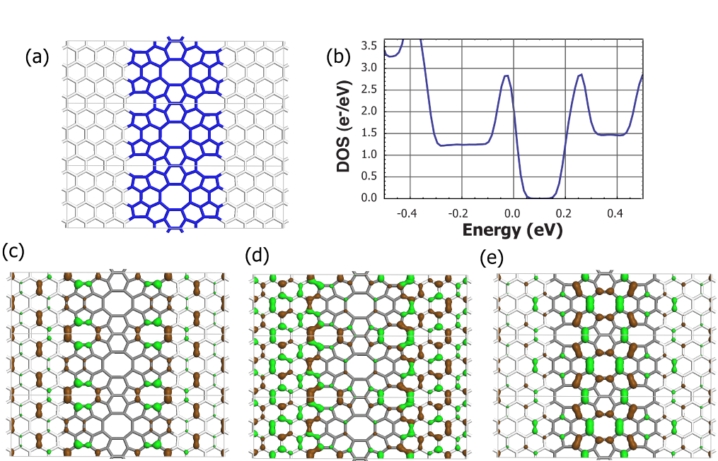
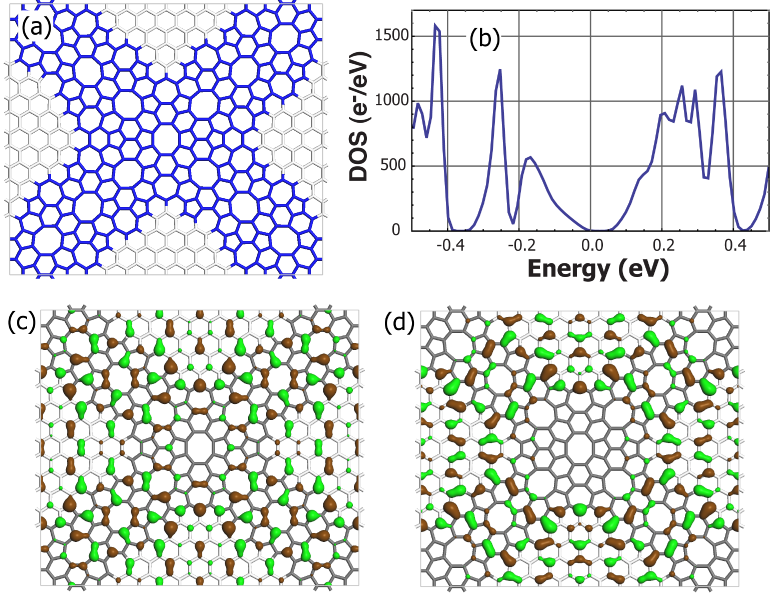
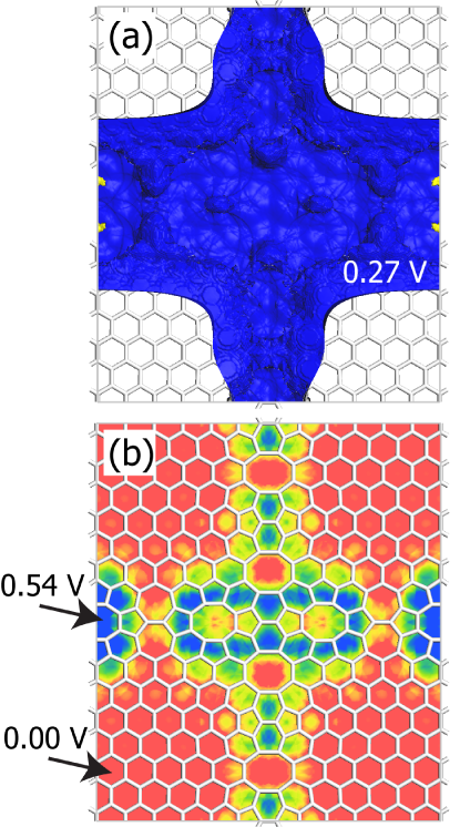
Embedded ribbons of semiconducting octite (Fig. 7) were subsequently investigated. The dimensions of the periodic cell were fixed to simulate a constraining lattice of graphene, and DFT was used to obtain the planar, ground state structure shown in Fig. 16(a). The DOS plot of Fig. 16(b) indicates that the ribbon endows the graphene with a 0.17 eV band gap, only slightly smaller than the 0.2 eV band gap of the octite SC itself. Unlike the metallic ribbon, the HOMO and LUMO states are not confined to the ribbon, although they do have contributions from orbitals along the interfaces between the two allotropes (Fig. 16(c, d)). Localized states appear along the edge of zigzag nanoribbons [52] and interestingly, the LUMO+1 state is highly localized within the ribbon as shown in Fig. 16(e).
The electronic structure of the semiconducting ribbon is further analyzed by plotting the electrostatic field. As shown in Fig. 17, potential isosurfaces tend to be more localized on the ribbon as the distance above the sheet increases. These potential surfaces are positive, indicating that additional charge will be attracted to the semiconducting ribbons.
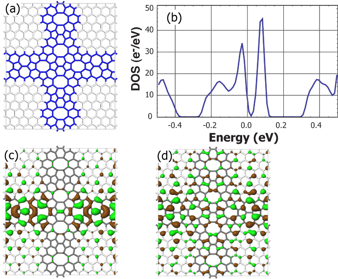
Embedded ribbons may be constructed with a variety of chiralities, and this can be exploited to create junctions and ribbon networks. Two examples of such semiconductor networks are considered. The first is shown in Fig. 18(a), where the enforcement of periodic boundary conditions gives graphene islands in the shape of diamonds. For this orientation of ribbons, the DOS plot indicates that the sheet still maintains a small band gap ( 0.05 eV). The HOMO state is localized within the ribbons with the exception of the ribbon junction, while the LUMO state shows that the first excited state will tend to avoid the junction completely.
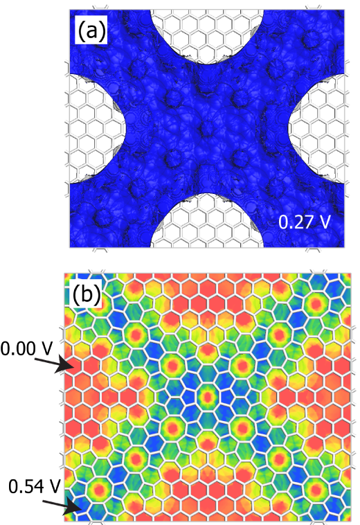
The electrostatic potential of the diamond network is shown in Fig. 19. Consistent with the results for isolated allotrope interfaces, potential surfaces lying furthest above the sheet are positive and localized on the ribbon network. Higher energy excited electrons should therefore be attracted to these conduction channels.
Perhaps not surprisingly, the orientation of intersecting ribbons impacts the electronic structure of the sheet. This is made clear by considering a second network of semiconducting ribbons which now partitions the graphene into rectangular islands. Figure 20(a) shows the planar, ground state geometry. The DOS of this system (panel b) indicates that the band gap is essentially lost. The HOMO state is now localized along the horizontal semiconducting ribbon (panel c), but the two states of immediately lower energy do not show localization along either ribbon orientation. This suggests that the two orientations have fundamentally different electronic properties which likely extends to their respective electron mobilities.
The electrostatic potential of the rectangular network, shown in Fig. 21, is very similar to that of the diamond networked sheet. Once again, potential surfaces lying furthest above the sheet are positive and localized on the ribbon network. Higher energy excited electrons should therefore be attracted to these conduction channels. The electrostatic contours of Fig. 21(c), though, show that the horizontal ribbon attracts electrons more strongly at a fixed height above the sheet.
5 Conclusions
Defect engineering offers a means of changing the electronic character of graphene without the need to introduce new atomic elements. An algebraic framework has been identified for the modification of lattices and is based on four basic actions which can be performed with a carbon dimer: bond rotation (STW defect); dimer addition (ISTW defect); dimer removal (divacancy defect); and no action (standard graphene dimer). These dimer actions can be combined to build a variety of localized defect structures; the current work has focused on the templating of elements to create extended defects. Two-dimensional templates can be used to create graphene allotropes. While most of these are good conductors, we have identified a defect structure which opens up a band gap of 1.2 eV. These allotropes can be created as conducting and semiconducting ribbons within graphene, extended one-dimensional defect structures. Their electronic character is largely preserved for even the thinnest ribbons, which offers the prospect of designing electronic components crafted entirely out of carbon.
6 Acknowledgements
We are pleased to acknowledge the use of computing resources provided through the Golden Energy Computing Organization (NSF Grant No. CNS-0722415) and the Renewable Energy MRSEC program (NSF Grant No. DMR-0820518) at the Colorado School of Mines. LDC thanks the Institute for Advanced Study at Tsinghua University where part of this work was completed.
References
- [1] Taisuke Ohta, Aaron Bostwick, Thomas Seyller, Karsten Horn, and Eli Rotenberg. Controlling the electronic structure of bilayer graphene. Science, 313(5789):951–954, 2006.
- [2] Gianluca Giovannetti, Petr A. Khomyakov, Geert Brocks, Paul J. Kelly, and Jeroen van den Brink. Substrate-induced band gap in graphene on hexagonal boron nitride: Ab initio density functional calculations. Physical Review B (Condensed Matter and Materials Physics), 76(7):073103, 2007.
- [3] Soon-Yong Kwon, Cristian V. Ciobanu, Vania Petrova, Vivek B. Shenoy, Javier Bareo, Vincent Gambin, Ivan Petrov, and Suneel Kodambaka. Growth of semiconducting graphene on palladium. Nano Letters, 9(12):3985 – 3990, 2009.
- [4] Yuanbo Zhang, Joshua P. Small, William V. Pontius, and Philip Kim. Fabrication and electric-field-dependent transport measurements of mesoscopic graphite devices. Applied Physics Letters, 86(7):073104, 2005.
- [5] Johan Nilsson, A. H. Castro Neto, F. Guinea, and N. M. R. Peres. Transmission through a biased graphene bilayer barrier. Physical Review B (Condensed Matter and Materials Physics), 76(16):165416, 2007.
- [6] L. Brey and H. A. Fertig. Electronic states of graphene nanoribbons studied with the dirac equation. Physical Review B (Condensed Matter and Materials Physics), 73(23):235411, 2006.
- [7] E. R. Mucciolo, A. H. Castro Neto, and C. H. Lewenkopf. Conductance quantization and transport gaps in disordered graphene nanoribbons. Phys. Rev. B, 79(7):075407, Feb 2009.
- [8] Jingwei Bai, Xing Zhong, Shan Jiang, Yu Huang, and Xiangfeng Duan. Graphene nanomesh. Nature Nanotechnology, 5:190 – 194, 2010.
- [9] Jorge O. Sofo, Ajay S. Chaudhari, and Greg D. Barber. Graphane: A two-dimensional hydrocarbon. Physical Review B (Condensed Matter and Materials Physics), 75(15):153401, 2007.
- [10] Dmitriy A. Dikin, Sasha Stankovich, Eric J. Zimney, Richard D. Piner, Geoffrey H. B. Dommett, Guennadi Evmenenko, SonBinh T. Nguyen, and Rodney S. Ruoff. Preparation and characterization of graphene oxide paper. NATURE, 448(7152):457–460, JUL 26 2007.
- [11] Lijie Ci, Li Song, Chuanhong Jin, Deep Jariwala, Dangxin Wu, Yongjie Li, Anchal Srivastava, Z. F. Wang, Kevin Storr, Luis Balicas, Feng Liu, and Pulickel M. Ajayan. Atomic layers of hybridized boron nitride and graphene domains. NATURE MATERIALS, 9(5):430–435, MAY 2010.
- [12] G. M. Rutter, J. N. Crain, N. P. Guisinger, T. Li, P. N. First, and J. A. Stroscio. Scattering and Interference in Epitaxial Graphene. Science, 317(5835):219–222, 2007.
- [13] Mark T. Lusk and L. D. Carr. Nanoengineering defect structures on graphene. Physical Review Letters, 100(17):175503, 2008.
- [14] Mark T. Lusk and L.D. Carr. Creation of graphene allotropes using patterned defects. Carbon, 47(9):2226 – 2232, 2009.
- [15] L. Carr M.T. Lusk, D.T. Wu. Graphene nanoengineering and the inverse-stone-thrower-wales defect. Physical Review B, 85:155444, 2010.
- [16] Lincoln D. Carr and Mark T. Lusk. Defect engineering: Graphene gets designer defects. Nature Nanotechnology, 5(5):316 – 317, 2010.
- [17] M. Sternberg, L. A. Curtiss, D. M. Gruen, G. Kedziora, D. A. Horner, P. C. Redfern, and P. Zapol. Carbon ad-dimer defects in carbon nanotubes. Phys. Rev. Lett., 96:075506, 2006.
- [18] Julio A. Rodriguez-Manzo and Florian Banhart. Creation of individual vacancies in carbon nanotubes by using an electron beam of 1 ådiameter. Nano Letters, 9(6):2285 2289, 2009.
- [19] F. Schedin, A. K. Geim, S. V. Morozov, E. W. Hill, P. Blake, M. I. Katsnelson, and K. S. Novoselov. Direct evidence for atomic defects in graphene layers. Nature, 430:870–873, 2007.
- [20] Koki Urita, Kazu Suenaga, Toshiki Sugai, Hisanori Shinohara, and Sumio Iijima. In situ observation of thermal relaxation of interstitial-vacancy pair defects in a graphite gap. Phys. Rev. Lett., 94(15):155502, Apr 2005.
- [21] Jayeeta AU Lahiri, You Lin, Pinar Bozkurt, Ivan I. Oleynik, and Matthias Batzill. An extended defect in graphene as a metallic wire. Nature Nanotechnology, 5(5):326–329, 2010.
- [22] L. Li, S. Reich, and J. Robertson. Defect energies of graphite: Density-functional calculations. Phys. Rev. B, 72(18):184109, Nov 2005.
- [23] A. Stone and D. J. Wales. Theoretical studies of icosahedral c60 and some related species. Chem. Phys. Lett., 128(1):501–503, 1986.
- [24] J. Kotakoski, A. V. Krasheninnikov, and K. Nordlund. Energetics, structure, and long-range interaction of vacancy-type defects in carbon nanotubes: Atomistic simulations. Phys. Rev. B, 74(24):245420, Dec 2006.
- [25] Gunn Kim, Byoung Wook Jeong, and Jisoon Ihm. Deep levels in the band gap of the carbon nanotube with vacancy-related defects. Applied Physics Letters, 88(19):193107, 2006.
- [26] M. Berthe, S. Yoshida, Y. Ebine, K. Kanazawa, A. Okada, A. Taninaka, O. Takeuchi, N. Fukui, H. Shinohara, S. Suzuki, K. Sumitomo, Y. Kobayashi, B. Grandidier, D. Stievenard, and H. Shigekawa. Reversible defect engineering of single-walled carbon nanotubes using scanning tunneling microscopy. Nano Letters, 7(12):3623–3627, 2007.
- [27] Y. Sugimoto, M. Abe, S. Hirayama, N. Oyabu, O. Custance, and S. Morita. Atom inlays performed at room temperature using atomic force microscopy. Nature Materials, 4:156, 2005.
- [28] Jianhui Yuan and K.M. Liew. Effects of vacancy defect reconstruction on the elastic properties of carbon nanotubes. Carbon, 47(6):1526 – 1533, 2009.
- [29] M. Sammalkorpi, A. Krasheninnikov, A. Kuronen, K. Nordlund, and K. Kaski. Mechanical properties of carbon nanotubes with vacancies and related defects. Phys. Rev. B, 70(24):245416, Dec 2004.
- [30] D. G. Allis and K. E. Drexler. Design and analysis of a molecular tool for carbon transfer in mechanosynthesis. J. Comput. Theor. Nanosci., 2:45, 2005.
- [31] D. Appelhans. Eight-membered carbon rings in graphene allotropes to enhance stability and generate semiconductors. M.S. Thesis, 2009.
- [32] D. J. Appelhans, Z. Lin, and M. T. Lusk. A two-dimensional carbon semiconductor. Physical Review B, 2010, submitted.
- [33] B. Delley. An all-electron numerical-method for solving the local density functional for polyatomic-molecules. Journal of Chemical Physics, 92(1):508–517, JAN 1 1990.
- [34] John P. Perdew and Yue Wang. Accurate and simple analytic representation of the electron-gas correlation energy. Phys. Rev. B, 45(23):13244 – 13249, Jun 1992.
- [35] G. Kresse and J. Hafner. Ab initio molecular dynamics for liquid metals. Phys. Rev. B, 47(1):558–561, Jan 1993.
- [36] G. Kresse and J. Hafner. Ab initio molecular-dynamics simulation of the liquid-metal–amorphous-semiconductor transition in germanium. Phys. Rev. B, 49(20):14251–14269, May 1994.
- [37] G. Kresse and J. Furthm ller. Efficiency of ab-initio total energy calculations for metals and semiconductors using a plane-wave basis set. Computational Materials Science, 6(1):15 – 50, 1996.
- [38] G. Kresse and J. Furthmüller. Efficient iterative schemes for ab initio total-energy calculations using a plane-wave basis set. Phys. Rev. B, 54(16):11169–11186, Oct 1996.
- [39] P. E. Blöchl. Projector augmented-wave method. Phys. Rev. B, 50(24):17953–17979, Dec 1994.
- [40] G. Kresse and D. Joubert. From ultrasoft pseudopotentials to the projector augmented-wave method. Phys. Rev. B, 59(3):1758–1775, Jan 1999.
- [41] John P. Perdew, J. A. Chevary, S. H. Vosko, Koblar A. Jackson, Mark R. Pederson, D. J. Singh, and Carlos Fiolhais. Atoms, molecules, solids, and surfaces: Applications of the generalized gradient approximation for exchange and correlation. Phys. Rev. B, 46(11):6671–6687, Sep 1992.
- [42] M. Shishkin and G. Kresse. Self-consistent gw calculations for semiconductors and insulators. PHYSICAL REVIEW B, 75(23):235102, JUN 2007.
- [43] M. C. Payne, M. P. Teter, D. C. Allan, T. A. Arias, and J. D. Joannopoulos. Iterative minimization techniques for ab initio total-energy calculations: molecular dynamics and conjugate gradients. Rev. Mod. Phys., 64(4):1045–1097, Oct 1992.
- [44] A. A. El-Barbary, R. H. Telling, C. P. Ewels, M. I. Heggie, and P. R. Briddon. Structure and energetics of the vacancy in graphite. Phys. Rev. B, 68(14):144107, Oct 2003.
- [45] K. S. Novoselov, A. K. Geim, S. V. Morozov, D. Jiang, Y. Zhang, S. V. Dubonos, I. V. Grigorieva, and A. A. Firsov. Electric Field Effect in Atomically Thin Carbon Films. Science, 306(5696):666–669, 2004.
- [46] Vincent H. Crespi, Lorin X. Benedict, Marvin L. Cohen, and Steven G. Louie. Prediction of a pure-carbon planar covalent metal. Phys. Rev. B, 53(20):R13303–R13305, May 1996.
- [47] H. Terrones, M. Terrones, E. Hern ndez, N. Grobert, J. C. Charlier, and P. M. Ajayan. New metallic allotropes of planar and tubular carbon. Phys. Rev. Lett., 84:1716–1719, 2000.
- [48] Hendrik J. Monkhorst and James D. Pack. Special points for brillouin-zone integrations. Phys. Rev. B, 13(12):5188–5192, Jun 1976.
- [49] Melinda Y. Han, Barbaros Ozyilmaz, Yuanbo Zhang, and Philip Kim. Energy band-gap engineering of graphene nanoribbons. Physical Review Letters, 98(20):206–805, 2007.
- [50] Eduardo V. Castro, María P. López-Sancho, and María A. H. Vozmediano. New type of vacancy-induced localized states in multilayer graphene. Phys. Rev. Lett., 104(3):036802, Jan 2010.
- [51] G. J. Ackland. Embrittlement and the bistable crystal structure of zirconium hydride. Phys. Rev. Lett., 80(10):2233–2236, Mar 1998.
- [52] Kyoko Nakada, Mitsutaka Fujita, Gene Dresselhaus, and Mildred S. Dresselhaus. Edge state in graphene ribbons: Nanometer size effect and edge shape dependence. Phys. Rev. B, 54(24):17954–17961, Dec 1996.