Spin transport through a quantum network: Effects of Rashba spin-orbit interaction and Aharonov-Bohm flux
Abstract
We address spin dependent transport through an array of diamonds in the presence of Rashba spin-orbit (SO) interaction where each diamond plaquette is penetrated by an Aharonov-Bohm (AB) flux . The diamond chain is attached symmetrically to two semi-infinite one-dimensional non-magnetic metallic leads. We adopt a single particle tight-binding Hamiltonian to describe the system and study spin transport using Green’s function formalism. After presenting an analytical method for the energy dispersion relation of an infinite diamond chain in the presence of Rashba SO interaction, we study numerically the conductance-energy characteristics together with the density of states of a finite sized diamond network. At the typical flux , a delocalizing effect is observed in the presence of Rashba SO interaction, and, depending on the specific choices of SO interaction strength and AB flux the quantum network can be used as a spin filter. Our analysis may be inspiring in designing spintronic devices.
pacs:
73.23.-b, 72.25.-bI Introduction
In recent times spin transport in low dimensional systems has drawn much attention both from theoretical as well as experimental point of view, due to its promising applications in the field of ‘spintronics’ spintronics . It is a newly developed sub-discipline in condensed matter physics, that deals with the idea of manipulating spin of the electrons in transport phenomena in addition to their charge, and holds future promises to integrate memory and logic into a single device. Since the discovery of Giant Magnetoresistance (GMR) effect gmr in Fe-Cr magnetic multilayers revolutionary advancement has taken place in data processing, device making and quantum computation techniques. Today generation of pure spin current is a major challenge to us for further development in quantum computation. A more or less usual way of realization trend1 ; trend2 of spin filters is by using ferromagnetic leads or by external magnetic field. But in the first case, spin injection from ferromagnetic leads is difficult due to large resistivity mismatch and for the second one the difficulty is to confine a very strong magnetic field into a small region, like, a quantum dot (QD). Therefore, attention is now being paid for modeling of spin filters using the intrinsic properties intrinsic1 ; intrinsic2 ; intrinsic3 ; intrinsic4 ; intrinsic5 ; intrinsic6 of the mesoscopic systems such as spin-orbit interaction or voltage bias. Studies on Rashba spin orbit interaction rashba1 ; rashba2 ; rashba3 ; rashba4 , which is present in asymmetric heterostructures has made a significant impact in semiconductor spintronics as far as the control of spin dynamics is concerned. It is generally important in narrow gap semiconductors and its strength can be tuned by electrostatic means, e.g., applying external gate voltages gate1 ; gate2 ; gate3 . Rashba SO interaction induces spin flipping through a mechanism known as D’yakonov-Perel’ Dyakonov mechanism, which is a slow spin scattering process in which spin precession takes place around the Rashba field during transmission.
Over the last few years quantum networks are becoming prospective candidates for studying transport phenomena because of the manifestation of several interesting features, like, quantum interference, interplay of AB flux and network geometry on electron localization, spin-orbit interaction induced delocalization, effect of disorder, electron-electron interaction, etc. In 2000, Vidal et al. have shown Hubbard interaction can destroy the localization induced by magnetic field in a diamond network vidal1 . In some other works vidal2 ; vidal3 they studied the general formalism to obtain conductance of any quantum networks and the effect of disorder and interaction. Latter in 2002, they considered Josephson-junction chain of diamonds in a magnetic field to show a local symmetry at half flux-quantum vidal4 . It may be interesting to study the effects of Rashba SO coupling and AB flux in such quantum networks. Depending on their topology these geometries exhibit various striking spectral properties, and the interplay between AB flux and Rashba SO strength can also be explored. In 2005, Bercioux et al. bercioux considered the effect of AB flux and Rashba SO interaction on the energy averaged conductances of a finite sized diamond chain. They observed that in such a network spin-orbit interaction or AB flux can induce complete localization, while the presence of both of them can lead to the effect of weak anti-localization. The possibility to use such a diamond network as a spin filter was explored by Aharony et al. in 2008 aharony . In 2009, there was another work by Chakrabarti et al. sil , where they have shown how such a diamond network can be implemented as a p-type or n-type semiconductor depending on the suitable choice of the on-site potentials of the atoms at the vertices of the network and the strength of magnetic flux penetrating each diamond plaquette. But the effect of spin-orbit interaction was not considered. Several other interesting theoretical works have been done considering this kind of geometry. Gulacsi et al. gul1 ; gul2 in 2007 shown the exact ground state of diamond Hubbard chain in magnetic field exhibits a wide range of striking properties, those are tunable by magnetic flux, electron density, etc. Peeters et al. considered quantum rings in presence of Rashba SO interaction and magnetic field to obtain various features of magnetoconductance peeters1 ; peeters2 ; peeters3 . In our present work, we wish to explore the spectral and transport properties of a diamond network in the presence of both AB flux and Rashba SO interaction. We calculate spin conserved and spin flip conductances using single-particle Green’s function formalism green1 within a tight-binding framework for a finite sized diamond chain, which is compatible with the analytical dispersion relation obtained by renormalization group method for an infinite diamond network. Analysis of the spin-dependent conductances, dispersion relation and the density of states (DOS) provides an insight about the effect of Rashba SO interaction and AB flux on the localization behavior of the electrons. Finally, we show that, for some specific choices of the external parameters this finite sized diamond network can achieve a high degree of spin polarization.
Our organization of the paper is as follows. Following a brief introduction (Section I), in Section II, we present the model and the theoretical formulation. Section III is on our work comprising an analytical form for the energy dispersion relation for an infinite diamond network, the numerical calculations of two-terminal conductance, DOS, discussion on delocalizing effect in presence of SO interaction and demonstration of spin filtering action for a finite sized diamond array. At the end, the summary of our work will be available in Section IV.
II Model and theoretical formulation
At the beginning of our theoretical formulation we start by describing the geometry of the quasi one-dimensional nanostructure through which spin transport properties are being investigated. In Fig. 1 we illustrate schematically the quantum network, in which the square loops are connected at the vertices (termed as Diamond Network (DN) or
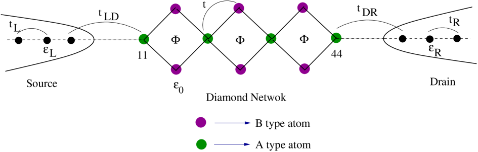
Diamond Chain (DC)). The diamond array is connected symmetrically to two semi-infinite one-dimensional (D) non-magnetic metallic leads, commonly known as source and drain which are characterized by the electrochemical potentials and under the non-equilibrium condition when a bias voltage is applied.
The full Hamiltonian for the complete system, i.e., source-DN-drain can be written as,
| (1) |
where, represents the Hamiltonian for the diamond network. corresponds to the Hamiltonian for the left (right) lead, i.e., source (drain), and is the Hamiltonian describing the chain-lead coupling.
We model the diamond network by the nearest-neighbor tight-binding Hamiltonian which in Wannier basis can be written as,
| (2) | |||||
where,
=
=
=
=
=.
Here is the site energy of each atomic site of the diamond
chain. For type of atoms , while for type
of atoms we call as (see Fig. 1).
The second and third terms represent the electron hopping along
and directions, respectively, where is the nearest-neighbor
hopping strength and is the phase factor
due to the magnetic flux threaded by each diamond plaquette. Here
we use double indexing to describe the location of lattice sites in the
diamond network, as illustrated in Fig. 2 for a single plaquette.
The fourth and fifth terms are associated with the spin dependent Rashba
interaction, where is the isotropic nearest-neighbor transfer
integral that measures the strength of Rashba SO coupling.
Similarly, the Hamiltonian for the two leads can be written as,
| (3) |
Here also,
=
=
where, is the site energy and is the
hopping strength between the nearest-neighbor sites in the left (right)
lead.
The diamond chain-to-lead coupling Hamiltonian is described by,
| (4) |
where, being the chain-lead coupling strength.
In order to calculate spin dependent transmission probabilities through the quantum network, we use single particle Green’s

function formalism. Within the regime of coherent transport and in absence of Coulomb interaction this technique is well applied.
The single particle Green’s function representing the full system for an electron with energy is defined as,
| (5) |
where .
The matrix representation for the Hamiltonian can be expressed as
| (6) |
where, , and are the Hamiltonian matrices for the left lead, diamond network and right lead, respectively. and are the coupling matrices between diamond network and the leads. Since there is no direct coupling between the leads themselves, the corner elements of are null matrices. A similar definition holds true for the Green’s function matrix as well.
| (7) |
The problem of finding in the full Hilbert space of can be mapped exactly to a Green’s function corresponding to an effective Hamiltonian in the reduced Hilbert space of diamond network and we have
| (8) |
where, and represent the contact self-energies introduced to incorporate the effects of semi-infinite leads coupled to the system. The self-energies are expressed by the relations,
| . | (9) |
Thus, the form of self-energies are independent of the nano-structure itself through which transmission is studied and they completely describe the influence of the two leads attached to the system. Now, the transmission probability of an electron with energy is related to the Green’s function as,
| (10) | |||||
where, = , = and . Here, and are the retarded and advanced single particle Green’s functions for an electron with energy . and are the coupling matrices, representing the coupling of the quantum network to the left and right leads, respectively, and they are defined by the relation,
| (11) |
Here, and are the retarded and advanced self-energies, respectively, and they are conjugate to each other. It is shown in literature by Datta et al. green1 that the self-energy can be expressed as a linear combination of a real and an imaginary part in the form,
| (12) |
The real part of self-energy describes the shift of the energy levels and the imaginary part corresponds to the broadening of the levels. The finite imaginary part appears due to incorporation of the semi-infinite leads having continuous energy spectrum. Therefore, the coupling matrices can easily be obtained from the self-energy expression and is expressed as,
| (13) |
Considering linear transport regime, conductance is obtained using two-terminal Landauer conductance formula,
| (14) |
Throughout our study we choose for simplicity.
III Numerical results and discussion
In this section we study spin dependent transport through a diamond chain in presence of Rashba spin orbit interaction and magnetic flux and investigate the interplay between them. An array of diamonds is a bipartite structure
with lattice sites having different co-ordination numbers. Electron localization plays a significant role even in the absence of disorder in this kind of geometry due to quantum interference effect. First we obtain analytically the dispersion relation for an infinite diamond chain in the presence of magnetic flux and Rashba interaction. Next, we simulate numerically various features of spin transport using a finite size diamond chain. Before analyzing the results first we specify the values of the parameters those are used in the numerical simulations. We consider that the two non-magnetic side-attached leads are made up of identical materials. The on-site energies in the two leads () are set to . Hopping strength between the sites in the leads is chosen as , whereas in the diamond chain it is set as . The Rashba strength () is chosen to be uniform along and directions and throughout the calculation its magnitude is considered as comparable to . Energy scale is fixed in unit of . Throughout the analysis we present all the results considering the chain-to-electrode coupling strength as .
III.1 Energy dispersion relation in presence of Rashba SO interaction and magnetic flux
The energy dispersion relation for an infinite diamond chain clearly depicts several significant features of this kind of topology. In order to study the - relation theoretically, first we map the quasi one-dimensional diamond network into a linear chain with modified site energy and hopping strength.
We start with the Schrodinger equation which can be cast in the form of a difference equation. For an arbitrary site (), where and denote the indexing along and directions, respectively, the difference equation can be expressed as
| (15) | |||||
where,
=
=
=
=
=;
=;
and
=
being the AB flux enclosed by each diamond plaquette,
being the wave function amplitude at the np-th site
with spin . , the elementary flux-quantum.
We begin the decimation technique by writing down the difference equations at the sites containing A and B type atoms (see Fig. 2). The equations are given below
| (16) |
and,
| (17) | |||||
Substituting , , and from Eq. (16) in Eq. (17) we get,
| (18) |
This represents the difference equation for an infinite linear chain with modified site energy and the forward and backward hopping strengths and , respectively. These quantities are expressed as follows.
As the translational invariance is preserved in this decimated infinite linear chain, the solution will be of Bloch form and can be written as,
| (20) |
being a short form of .
Using this form of , the difference equation for an arbitrary site can be expressed as,
| (25) | |||||
| (28) |
For the non-trivial solution of Eq. (LABEL:d7) we have the relation,
| (30) |
where, = .
Expanding Eq. (30) we obtain a -th degree polynomial in and solving it we get the - dispersion relation in terms of the parameters and . The solutions correspond to energy eigenstates which are linear combinations of up and down states.
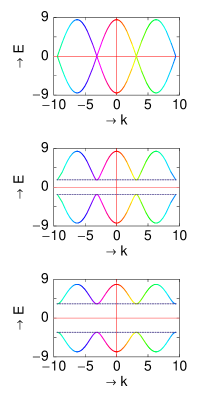
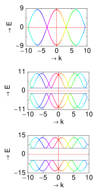
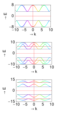
Following the above analytical treatment, in Fig. 3 we show the versus dispersion curves for some typical parameter values of and . The first column corresponds to the results for some specific values of AB flux in the absence of Rashba SO coupling, i.e., . It is observed that for zero magnetic flux the spectrum is degenerate and gapless, whereas a small non-zero flux opens a gap symmetrically around preserving the degeneracy. Here we choose and the gap appears symmetrically as long as is introduced, but the point is that for unequal values of and gap always appears even in the absence of (which is not shown in the figure). The width of the gap increases symmetrically with the rise in . In the second column of Fig. 3 we present the energy dispersion curves for the three different values of Rashba SO coupling strength keeping , where the upper, middle and lower spectra correspond to , and , respectively. The upper spectrum is gapless and degenerate as described earlier. For non-zero values of , the energy spectra get splitted vertically and all the degeneracies are removed except at the points , where , , , . The gap becomes widened with the increase in Rashba strength as clearly noticed from the middle and lower spectra. The above features seem to be more interesting when a non-zero magnetic flux is applied. In this case, each sub-band gets separated vertically as illustrated in the third column of Fig. 3. With a
sufficiently high magnetic flux () and Rashba strength () two additional gaps occur in the dispersion spectrum along with the previous one, and these gaps can be controlled externally by tuning the AB flux or the Rashba strength. We will show that these results are quite significant so far as the designing of nanoscale spintronic devices are concerned.
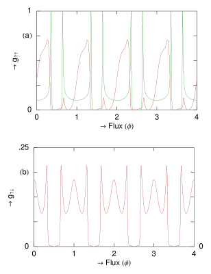
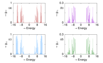
III.2 Variation of conductances with AB flux
In Fig. 4 we plot conductance-flux characteristics for a diamond network both in the presence and absence of Rashba SO interaction. The results are computed at a typical energy considering five diamond plaquettes, where the green and red curves correspond to and , respectively. It is observed that in the absence of Rashba coupling spin flip conductance drops exactly to zero for the entire range of (green curve in Fig. 4(b), coincides with the axis), while spin conserved conductance persists and it provides flux-quantum periodicity as a function of . Interestingly we see that completely vanishes at (see green curve of Fig. 4(a)) due to the complete destructive interference among the electronic waves passing through different arms of the plaquettes. On the other hand, in the presence of Rashba SO interaction both and have values for wide ranges of and a significant change in their amplitudes takes place compared to the case where . In the presence of the SO interaction, the oscillatory character of the conductances is still preserved providing traditional flux-quantum periodicity. The important feature is that even for non-zero value of , spin flip conductance disappears at . Since and exhibit exactly identical behavior to those mentioned for and , respectively, we do not display these results explicitly.
The above numerical results can be justified from the following mathematical analysis.
To illustrate the behaviors of AB oscillation both in the presence and absence of Rashba SO interaction, we consider an ideal D square loop threaded by an AB flux , as shown schematically in Fig. 5. Two semi-infinite one-dimensional leads are connected at the vertices P and Q of the square loop.

Rashba SO interaction is considered to be present only in the loop and not in the leads. If and describe the incoming and outgoing wave functions at the respective vertices P and Q, then can be obtained considering only st order tunneling processes as xie ,
| (31) |
where, . is the rotation operator defined by the relation,
| (32) |
where, is the spin precession angle. is the strength of Rashba SO interaction and represents the length of each side of the square loop. The wave functions and used in Eq. (31) are defined as follows.
and .
Following Eq. (32) the matrices and can be written as given below.
.
and
.
With these matrix forms we can express the wave functions and as linear combinations of and by expanding Eq. (31) as,
| (33) |
where, the co-efficients are functions of and .
Now the probability of getting an up spin electron at the point Q, for the incidence of an electron with up spin at the point P, i.e., the spin conserved transmission probability is proportional to , viz, . Similarly, the probability of getting a down spin electron with up spin incidence, i.e., the spin flip transmission probability is proportional to , viz, . After a few mathematical steps the quantities and are expressed as,
| (34) | |||||
and
| (35) |
In the absence of Rashba SO interaction and the above two equations can be simplified as follows.
| (36) |
and
| (37) |
With the last four mathematical expressions (Eqs. (34)-(37)) we can clearly justify the essential features those are presented in Fig. 4. In the absence of Rashba SO interaction, spin flip conductance vanishes for the entire range of (coincident green curve of Fig. 4(b) with axis) in accordance with Eq. (37). On the other hand, a oscillatory character of up spin conductance with periodicity in the absence of (green curve of Fig. 4(a)) follows from Eq. (36). The vanishing behavior of at the typical flux is also justified from Eq. (36). In the presence of SO interaction, both pure spin transmission and spin flip transmission get modified satisfying Eqs. (34) and (35), respectively. For finite value of , spin flip conductance always vanishes at obeying Eq. (35).
III.3 Conductance-energy characteristics
Now we focus our attention on the conductance-energy characteristics of a finite sized diamond network for some specific values of AB flux and Rashba SO interaction strength .
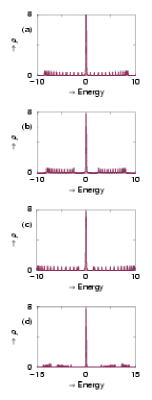
In Fig. 6 we plot up spin conductances () as a function of injecting electron energy () for a diamond network
considering identical plaquettes in the absence of Rashba interaction. The top, middle and bottom spectra correspond to AB flux , and , respectively. When , the spectrum is gapless (Fig. 6(a)). The presence of opens a gap and the width of the gap increases with the rise in as evident from
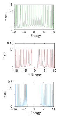
Figs. 6(b) and (c). This gap is symmetric around the energy with the choice . On the other hand, if the site energies and are unequal then a gap in the conductance spectrum appears (not shown in the figure) even in the absence of magnetic flux both for an infinite as well as for a finite sized diamond array. This gap will be symmetric across provided and are identical, and the width of the gap increases symmetrically about the center of the gap with the enhancement in . In this particular case we do not consider any Rashba interaction, and therefore, no spin flip transmission takes place.
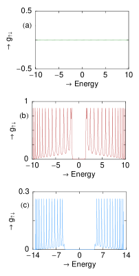
In Fig. 7 we show the conductance-energy characteristics of a diamond network with plaquettes for different values of in the absence of magnetic flux . The st, nd and rd rows correspond to the results when , and , respectively. The spin conserved conductances () are plotted in the first column, while in the second column spin flip conductances () are given. In absence of , gapless spectrum is observed for spin conserved conductance, while spin flip conductance vanishes for the entire energy range. For all other cases, a gap appears in the spectrum and its width can be regulated by tuning the Rashba coupling strength.
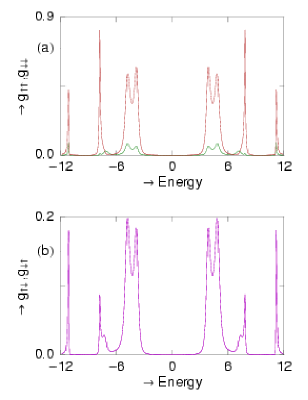
The most interesting features in the conductance-energy characteristics are observed when we consider the effects of both the AB flux and Rashba SO coupling . The results are shown in Fig. 8 for a diamond chain with identical diamond plaquettes for and . For sufficiently high AB flux and Rashba strength, two additional energy gaps occur at the flanks on both sides of the conductance spectrum in addition to the central gap. The energy gaps are positioned identically in all these spectra.
It is important to note that when anyone of and is zero and other is non-zero, becomes exactly identical to , and so is and . On the other hand, when both are non-zero, spin conserved conductances differ in magnitude, but the spin flip conductances remain identical. All these conductance-energy characteristics shown in Figs. 6-8 are compatible with the - diagrams presented in Fig. 3. The gaps of the conductance spectra of finite sized diamond chain compare well with those of the dispersion curves obtained earlier for an infinite sized diamond chain.
III.4 DOS-energy characteristics
To gain insight into the nature of energy eigenstates of such a quantum network we address the behavior of average density of states. It is expressed as,
| (38) |
where, being the total number of atomic sites in the diamond chain.
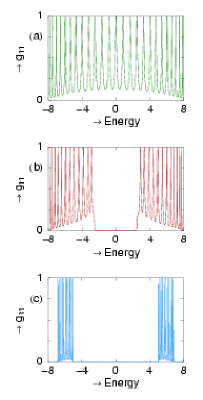
As illustrative examples, in Fig. 9 we present the variations of average density of states as a function of energy for a diamond chain
consisting of plaquettes for different values of AB flux and Rashba SO coupling strength . In (a), - spectrum is given when both and are fixed at zero. The spectrum does not exhibit any gap as expected when . A sharp peak is observed at the band center, i.e., at due to localized states. These localized states are highly degenerate and in general pinned at the energy . The existence of the localized state is a characteristic feature of diamond network as mentioned in an earlier work sil . In (b) and (c), energy gaps appear symmetrically around the central peak at by the AB flux and Rashba coupling strength , respectively. By tuning the AB flux or Rashba coupling strength , the width of the gap can be controlled. Finally, in (d) we display average DOS when both and are finite. In such situation two extra gaps appear together with the central ones. The localized states are still situated at the same place as earlier.
III.5 Effect of Rashba spin-orbit interaction on localization
In such a quantum network, AB flux can induce complete localization. At , conductance drops exactly to zero in the absence of Rashba SO interaction. This is due to the complete
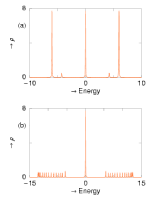
destructive interference between the electronic waves passing through different arms of the network. At , two more sharp peaks appear in the - characteristics due to localized states (Fig. 10(a)) in addition to the previous one pinned at . The positions of these localized states can be evaluated exactly and they are expressed mathematically as,
| (39) |
In the presence of Rashba spin orbit interaction, the interference is not completely destructive anymore at . The two additional peaks at the opposite sides of the central one disappear for non-zero Rashba strength as clearly seen from Fig. 10(b). Rashba spin-orbit coupling affects the spin dynamics significantly resulting in a non-zero conductance at .
III.6 Rashba induced semi-conducting behavior
Here we address how Rashba SO interaction can induce semi-conducting behavior in such a quantum network in the absence of . A similar type of semi-conducting nature controlled by AB flux has been established in such a system, where SO interaction was not considered sil . To establish our idea, in
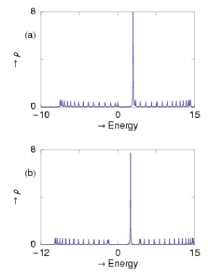
Fig. 11 we plot the average density of states as a function of energy considering plaquettes where and are set at and , respectively. When and are not same, the diamond network possesses an intrinsic gap in the energy spectrum even in the absence of and , as evident from Fig. 11(a). The sharp peak in the DOS is situated at the edge of the gap, and it actually corresponds to the localized states. By controlling the external gate potential, i.e., tuning the Rashba strength to a non-zero value, the width of the gap can be increased arbitrarily as shown in Fig. 11(b), keeping the position of the localized states invariant. Now, if the Fermi level is fixed at where we have localized states (see Fig. 11(b)), then for small Rashba coupling strength the gap between the localized level and the bottom of the right sub-band can be made small enough for the electrons to bridge. Therefore, the system behaves as a -type semiconductor. Similarly, if is fixed at and the Fermi level is set at the top of the left sub-band, then the system can be implemented equivalently as a -type semiconductor. In this case holes are created in the left sub-band. It is important to mention that when the site energies ( and ) are fixed at the same value, then also the system can be used as a semi-conductor depending on the electron concentration. The detailed analysis is available in Ref. sil .
III.7 Spin filtering action
With proper tuning of the external parameters like, magnetic flux and Rashba strength , a diamond network can achieve a high degree of spin polarization as discussed earlier in a theoretical work by Aharony et al. aharony . Here, we discuss this feature from a different point of view.
When there is no external magnetic field or magnetic flux, time reversal symmetry is not broken, and the Hamiltonian of the system remains
invariant under time reversal operation. Mathematically it is expressed as , where is the time reversal operator. The Rashba Hamiltonian () is usually written as,
| (40) | |||||
and , being the complex conjugation operator. The second quantized form of Eq. (40) is given by the fourth and fifth terms of Eq. (2). As electrons are spin- particles, so following Kramer’s theorem, each eigenstate is at least two-fold degenerate and spin is no longer a good quantum number in the presence of spin-orbit interaction. In many cases the degeneracy implied by Kramer’s theorem is merely the degeneracy between states of spin up and spin down, or something equally obvious. The theorem is non-trivial for a system with spin-orbit coupling in an unsymmetrical electric field, so that neither nor angular momentum is conserved. Kramer’s theorem implies that no such field can split the degenerate pairs of energy levels ballen .
However, the degeneracy can be removed by applying external magnetic flux or magnetic field as in this case time reversal symmetry is not conserved anymore and therefore spin polarization can be achieved. The degree of polarization of the transmitted electrons is conventionally defined as,
| (41) |
For our illustrative purpose, in Fig. 12 we plot the variations of conductances as a function of energy for a diamond network with three plaquettes considering and . A significant change is observed in the magnitudes of spin conserved conductances ( and ) (Fig. 12(a)), while the spin flip conductances ( and ) are identical as shown in Fig. 12(b). Therefore, applying a non-zero flux spin polarization is clearly obtained. Following Eq. (41) we calculate the degree of polarization for an arbitrary energy (say), and it is about .
IV Closing remarks
To conclude, in the present work we have explored spin dependent transport through an array of diamonds where Rashba SO interaction is present and each diamond plaquette is threaded by an AB flux . The diamond chain is directly coupled to two semi-infinite D non-magnetic metallic leads, namely, source and drain. We have adopted a discrete lattice model within the tight-binding framework to describe the system and present calculations based on Green’s function formalism. We have obtained analytical expression for the - dispersion relation for an infinite diamond network with Rashba SO interaction, and, show explicitly the interplay of spin-orbit interaction and magnetic flux on its band structure. This analysis also gives insight about the presence of spin dependent localized and extended eigenstates which crucially controls the spin dependent transport through such device. This analytical study, in fact, provides us a very good understanding about the transport behavior of spins across a finite sized array of diamonds. It has been clearly established that how delocalizing effect sets in due to Rashba SO interaction when the AB flux is . Quite interestingly we show that depending on the specific choices of SO interaction strength and AB flux, the quantum network can be utilized as a spin filter.
In the present work we have ignored the effects of temperature, electron-electron correlation, electron-phonon interaction, disorder, etc. Here, we set the temperature at K, but the basic features will not change significantly even at low temperature as long as thermal energy () is less than the average level spacing of the diamond chain. In this model it is also assumed that the two side-attached non-magnetic leads have negligible resistance. Our presented results may be useful in designing spin based nano electronic devices.
References
- (1) S. A. Wolf, D. D. Awschalom, R. A. Buhrman, J. M. Daughton, S. von Molnar, M. L. Roukes, A. Y. Chtchelkanova, and D. M. Treger, Science 294, 1488 (2001).
- (2) M. N. Baibich, J. M. Broto, A. Fert, F. N. Van Dau, F. Petroff, P. Etienne, G. Creuzet, A. Friederich, and J. Chazelas, Phys. Rev. Lett. 61, 2472 (1998).
- (3) W. Long, Q. F. Sun, H. Guo, and J. Wang, Appl. Phys. Lett. 83, 1397 (2003).
- (4) P. Zhang, Q. K. Xue, and X. C. Xie, Phys. Rev. Lett. 91, 196602 (2003).
- (5) Q. F. Sun and X. C. Xie, Phys. Rev. B 91, 235301 (2006).
- (6) Q. F. Sun and X. C. Xie, Phys. Rev. B 71, 155321 (2005).
- (7) F. Chi, J. Zheng, and L. L. Sun, Appl. Phys. Lett. 92, 172104 (2008).
- (8) T. P. Pareek, Phys. Rev. Lett. 92, 076601 (2004).
- (9) W. J. Gong, Y. S. Zheng, and T. Q. Lü, Appl. Phys. Lett. 92, 042104 (2008).
- (10) H. F. Lü and Y. Guo, Appl. Phys. Lett. 91, 092128 (2007).
- (11) Y. A. Bychkov and E. I. Rashba, Sov. Phys. JETP 39, 78 (1984).
- (12) T. P. Pareek and P. Bruno, Phys. Rev. B 65, 241305(R) (2002).
- (13) F. Mireles and G. Kirczenow, Phys. Rev. B 64, 024426 (2001).
- (14) N. Hatano, R. Shirasaki, and H. Nakamura, Phys. Rev. B 75, 032107 (2007).
- (15) G. Lommer, F. Malcher, and U. Rossler, Phys. Rev. Lett. 60, 728 (1988).
- (16) J. Nitta, T. Akazaki, H. Takayanagi, and T. Enoki, Phys. Rev. Lett. 78, 1335 (1997).
- (17) C. Hu, J. Nitta, T. Akazaki, H. Takayanagi, J. Osaka, P. Pfeffer, and W. Zawadzki, Phys. Rev. B 60, 7736 (1999).
- (18) M. I. D’yakonov and V. I. Perel’, Sov. Phys. JETP 33, 1053 (1971).
- (19) J. Vidal, B. Doucot, R. Mosseri, and P. Butaud, Phys. Rev. Lett. 85, 3906 (2000).
- (20) J. Vidal, G. Montambaux, and B. Doucot, Phys. Rev. B 62, R16294 (2000).
- (21) J. Vidal, P. Butaud, B. Doucot, and R. Mosseri, Phys. Rev. B 64, 155306 (2001).
- (22) B. Doucot and J. Vidal, Phys. Rev. Lett. 88, 227005 (2002).
- (23) D. Bercioux, M. Governale, V. Cataudella, and V. M. Ramaglia, Phys. Rev. B 72, 075305 (2005).
- (24) A. Aharony, O. E. -Wohlman, Y. Tokura, and S. Katsumoto, Phys. Rev. B 78, 125328 (2008).
- (25) S. Sil, S. K. Maiti, and A. Chakrabarti, Phys. Rev. B 79, 193309 (2009).
- (26) Z. Gulácsi, A. Kampf, and D Vollhardt, Phys. Rev. Lett. 99, 026404 (2007).
- (27) Z. Gulácsi, A. Kampf, and D Vollhardt, Progr. Theor. Phys. Suppl. 176, 1 (2008).
- (28) P. Földi, O. Kálmán, M. G. Benedict, and F. M. Peeters, Nano Lett. 8, 2556 (2008).
- (29) P. Földi, O. Kálmán, and F. M. Peeters, Phys. Rev. B 80, 125324 (2009).
- (30) B. Molnár, P. Vasilopoulos, and F. M. Peeters, Phys. Rev. B 72, 075330 (2005).
- (31) S. Datta, Quantum Transport: Atom to Transistor, Cambridge University Press, Cambridge (2005).
- (32) Z. Zhu, Q. -F. Sun, B. Chen, and X. C. Xie, Phys. Rev. B 74, 085327 (2006).
- (33) L. E. Ballentine, Quantum Mechanics: A Modern Development, World Scientific Publishing, (1998).