Electric-Field-control of spin rotation in bilayer graphene
Abstract
The manipulation of the electron spin degree of freedom is at the core of the spintronics paradigm, which offers the perspective of reduced power consumption, enabled by the decoupling of information processing from net charge transfer. Spintronics also offers the possibility of devising hybrid devices able to perform logic, communication, and storage operations. Graphene, with its potentially long spin-coherence length, is a promising material for spin-encoded information transport. However, the small spin-orbit interaction is also a limitation for the design of conventional devices based on the canonical Datta-Das spin-FET. An alternative solution can be found in magnetic doping of graphene, or, as discussed in the present work, in exploiting the proximity effect between graphene and Ferromagnetic Oxides (FOs). Graphene in proximity to FO experiences an exchange proximity interaction (EPI), that acts as an effective Zeeman field for electrons in graphene, inducing a spin precession around the magnetization axis of the FO. Here we show that in an appropriately designed double-gate field-effect transistor, with a bilayer graphene channel and FO used as a gate dielectric, spin-precession of carriers can be turned ON and OFF with the application of a differential voltage to the gates. This feature is directly probed in the spin-resolved conductance of the bilayer.
Graphene has attracted much attention since its first experimental fabrication Novoselov et al. (2004), due to its exceptional electronic properties linked to the Dirac physics of its low-energy quasiparticles Neto et al. (2009). Thanks to its extremely high mobility Geim and Novoselov (2007), graphene is also a promising material for nanoelectronics, where however the presence of a semiconducting gap is required. One-dimensional graphene-related structures like nanoribbons Bai et al. (2009) and carbon nanotubes Seidel et al. (2005) have been employed succesfully for nanoelectronic devices, but their practical applications are limited by the need of single-atom precision in the definition of their transversal width and radius, respectively. Carbon-based materials like epitaxial graphene on SiC Michetti et al. (2010) and bilayer graphene Fiori and Iannaccone (2009) have been shown to be promising for the realization of tunneling Field-Effect Transistors (FETs), while the gap is not sufficient for conventional FETs Cheli et al. (2009, ).
Spin-orbit coupling plays a crucial role in spintronics, providing a way to manipulate electron spin by means of an external field. This is at the heart of most proposed spintronic devices, such as the Datta-Das spin-FET Datta and Das (1990). However, theoretical studies have shown that spin-orbit coupling in graphene is extremely small Min et al. (2006); Huertas-Hernando et al. (2006). Therefore, conventional spintronics mechanisms are not applicable to graphene. On the other hand, graphene is attractive for spintronics because of its long spin-coherence time Tombros et al. (2007). Moreover, simulations show that magnetic doping Jayasekera et al. (2010) in graphene, or edge functionalization in GNRs Son et al. (2006); Cantele et al. (2009), lead to spin-splitted bands and potentially to a semi-metal dispersion relation, particularly attractive for spintronic applications Žutić et al. (2004).
An alternative approach can come from the exploitation of the interfacial proximity with a ferromagnetic oxide. Indeeed, it has been proposed that a spin splitting (acting as an effective Zeeman field) can arise in graphene due to Exchange Proximity Interaction (EPI) between electrons in graphene and localized electrons in a FO layer adjacent to the graphene layer Semenov et al. (2007); Huegen et al. (2008). The effective Zeeman splitting (which has been estimated to be of the order of meV Huegen et al. (2008)) acts on the spin of graphene carriers inducing a precession around the magnetization axis of the FO. The same mechanism was proposed for bilayer graphene, and the modification of the electronic structure and of the magnetoresistance as a function of relative angle between the magnetization axes of the upper and lower FO spacers has been investigated Semenov et al. (2008). The spin filtering properties of bilayer graphene with multiple magnetic barriers with EPI were also investigated in Ref. Dell’Anna and Martino, 2009. However, the control on the spin-transport properties exerted by an electric field, driven by gates, has not yet been the subject of investigation.
It is possible to induce an energy gap in bilayer graphene by applying an electric field perpendicular to the graphene plane Ohta et al. (2006); Castro et al. (2007); Oostinga et al. (2008); Zhang et al. (2009) . For small kinetic energy, first valence and conduction band wavefunctions are driven towards different planes of the bilayer by the applied field. This means that electrons in the first valence and conduction band have different probabilities to be found on the upper and lower plane. Therefore, we can devise a way to tune the spin-rotation of carriers in the bilayer graphene by reversing the gate voltage.
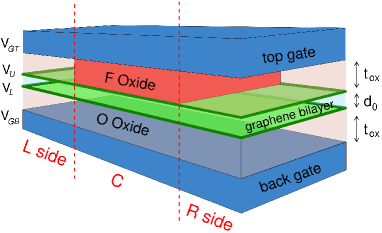
We consider a double gate bilayer graphene FET where a FO is used as the insulating layer between the bilayer graphene channel and the top gate, while an ordinary oxide (OO) is used as insulating layer for the bottom gate, as shown in Fig. 1. EPI interaction will mainly affect electrons on the upper graphene layer. By applying a direct or inverse differential voltage between the gates, we determine whether conduction electrons do or do not feel the EPI interaction, and whether the associated wavefunctions are quasi-localized either on the upper or on the lower plane. Consequently, we are able to switch on or off spin precession.
I Model
We discuss here in very generic terms the difference between an insulating material made of an ordinary oxide and of a FO. In both materials electrons reside in similarly localized wavefunctions, as it is proper of an insulating material, but in a FO they will be also characterized by a majority spin component. If we place a graphene sheet in proximity to a FO, rather than to a OO, in general we can expect a similar contribution for the direct Coulomb interaction between electrons in graphene and in the oxide, but a completely different contribution from the exchange interaction. Indeed, the exchange interaction requires “exchanged” electrons to have the same spin orientation, and therefore graphene electrons will feel a very different effective exchange proximity interaction (EPI) for majority and minority spin components with respect to the FO. Moreover, while the direct Coulomb interaction is long-ranged, EPI requires an overlap of the wavefunctions of “exchanged” particles. For this reason EPI interaction, as pointed out in Ref. Semenov et al., 2008, is essentially limited to the graphene layer placed in direct proximity to the FO, and it is negligible on more distant layers.
We assume here the simplest situation, in which a thin FO layer is deposited between the upper graphene plane and the top gate, with magnetization , and an OO layer is instead used as insulator between the lower graphene layer and the back gate (Fig. 1). The electronic states of bilayer graphene can be described, near the point, by the following Hamiltonian McCann (2006)
| (1) |
where and , with and the upper and lower layer potential, respectively, and is the value of the absolute elementary charge. In the future, let us denote with the index the variables relating to the upper (U) layer, and with the index those relating to the lower (L) layer. is the kinetic energy operator (with for the valley), is an effective energy term due to the EPI with the ferromagnetic insulators. We use the parameters eV Nilsson et al. (2008); Li et al. (2009), i.e. the bilayer interplane coupling, and m/s Barbier et al. (2009). Other interlayer coupling terms are neglected, in the spirit of Refs. Huegen et al., 2008; Semenov et al., 2008; Barbier et al., 2009, as they would not change the qualitative features of the phenomenon described in this work. The Hamiltonian acts on wavefunctions of the form
| (2) |
where , refer to the two inequivalent carbon atoms on the upper graphene layer, , to that of the lower layer. and are the channel dimensions along and directions. Now we distinguish the two spin components along the axis, perpendicular to the plane, therefore , with , , , , has to be regarded as a two-component spinor
| (3) |
The elements ,, , are diagonal in the spinor space, while off-diagonal terms can be due to the presence of an effective Zeeman field. If we imagine to put the upper graphene layer in contact with a ferromagnetic insulator having a polarization on the plane, the exchange interaction gives rise to an off-diagonal coupling in the spinor space of the kind
| (4) |
where is the versor of the magnetization vector . For simplicity, we assume for the upper layer a similar effective Zeeman coupling for the and sites, while EPI vanishes on the lower plane sites and .
II Bilayer Graphene
The idea of controlling spin rotation of bilayer graphene is essentially based on the plane-localization properties of the bilayer spinors, when a vertical field is applied. In particular, let us assume for a moment no EPI interaction, i.e. (). In this case the eigenvalues near the , or , point, are given by the formula McCann (2006)
| (5) |
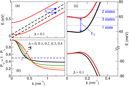
with , and with for the first () and second () conduction () or valence() band. The bilayer spinors, for a given and energy , are obtained by solving the linear system . In Fig. 2(a) we show the bilayer dispersion curve, compared with the graphene dispersion curves and , obtained by Eq. 5 by decoupling the two layers ().
In Fig. 2(b) we plot the projection of the first bilayer conduction band states () on the U plane. The behavior of the projection on the U plane can be easily understood from the bilayer dispersion curve. In fact, at , states of the first bilayer conduction band stand on the Dirac point of the U graphene layer. At , the and sublattices are not coupled by the kinetic term in the Hamiltonian in Eq. 1, therefore and sublattices are not mixed by and retain their original character. Correspondingly, the spinor of the first conduction band will have a weight on the sublattice. With increasing , the bilayer spinors have mixed contributions from the two planes and eventually, at sufficiently large , tends to a constant value. An explanation for this comes from the fact that for large , the bilayer conduction bands essentially originate from the mixing of only the n-type part of the Dirac cones for the U and L graphene sheets (shown in Fig. 2(a)), while contributions from the p-like part may be neglected. This leads to a two-level system with a fixed energy separation of , as plotted in Fig. 2(a), and fixed tunnel-coupling . The solutions of the two level system are , which correspond to the asymptotic behavior of bilayer conduction bands for large , and
| (6) |
for the first conduction band (), which explains the plateau in Fig. 2(b) at large . We note that, for a given , of the first conduction band corresponds to of the first valence band, and by reversing the potential of both layers one would perfectly exchange the projection properties of the two bands.
In Fig. 2(c), we plot the first conduction and valence band of a bilayer graphene subjected to EPI interaction as described by the Hamiltonian Eq. 1, with meV. When the EPI interaction is taken into account, electronic wavefuctions traveling on the U plane are subject to an effective Zeeman interaction, basically proportional to , that results in a spin splitting of the bilayer bands by . This proportionality clearly appears in Fig. 2(c), where we plot the conduction and valence bands of a bilayer graphene with a FO deposited on top of the U layer, considering a potential energy difference of eV between graphene layers. If we reverse , which can be realized by inverting the bias of top and back gates, the spin splitting of conduction and valence bands is inverted, as well as , and the Zeeman splitting at small will vanish in the conduction band. In a regime in which small states are responsible for transport through a FO-contacted bilayer region, we will therefore have a degree of control over the electron spin rotation induced by the effective Zeeman field.
III Transmission through a FO gated region
To calculate the spin rotation properties of our system we analyze the transmission through a region of the bilayer in which the EPI coupling is active, as is the case in Fig. 1. For simplicity, we imagine abrupt boundary conditions such that the contact with the FO is limited to the upper plane of the graphene bilayer from to . We consider an incoming conduction band electron from the left side (LS) () of given and therefore energy , with a chosen spin polarization. Elastic transmission through the active EPI zone conserves , because of the space homogeneity along the axis, but not the spin, and leads to reflected and transmitted components to the left and right side (RS) respectively (of and spin character).
In particular, the LS and RS are described by the Hamiltonian Eq. 1, with . We can here find, disregarding the spin which is here conserved, four possible values of the wavevector compatible with and energy : and , which are propagating modes, and , which can correspond alternatively to propagating modes or to evanescent modes, with a finite imaginary part Barbier et al. (2009). The number of propagating modes (with real wavevector) corresponds to the number of intersection points of the conduction bands with the horizontal line on Fig. 2(a). The remaining modes are evanescent. Therefore the total wavefunctions on the LS and RS can be written as
| (7) | |||||
| (8) |
where the matrices , and are built from the spinor set of the bilayer system in Eq. 1 without EPI. is the spin-polarization of the incoming particle and is a vector describing the component up and down with respect to the Z axis. Our calculation starts from fully polarized incoming particles, for which . For all matrices, rows run over the sublattices , while columns run over the left region output modes for , right region output modes for , and incoming modes for . The output coefficients are collected in
| (9) | |||||
| (10) |
with the tunneling coefficients for allowed modes in up or down spin orientation, and the reflection coefficients defined in a similar manner as .
In the central part of the system we have a mixing of spin components induced by the effective Zeeman splitting. Solving the secular equation for the Hamiltonian in Eq. 1 for a given energy and in-plane momentum , we obtain solutions for the wavevector with , …. The corresponding modes are described by the spinor where the index is used to specify that these states are for the system with Zeeman interaction. The scattering state in the central part of the system can be generally expressed as
| (11) |
The Dirac equation requires the continuity of spinors at the boundary and , which is now expressed by the following linear relations
| (12) | |||
| (13) |
with describing the phase accumulation of the different components of the scattering state by traveling through the C region. After elimination of , the problem is reduced to the solution of a linear system of the kind , with , which can be easily solved by standard numerical techniques. In practice, a source term , describing the incoming particle, pumps the linear system described through the dynamical matrix , which carries all the information about the transmission through the central region, and determines the output steady state described by .
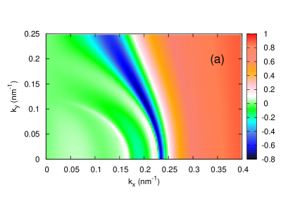
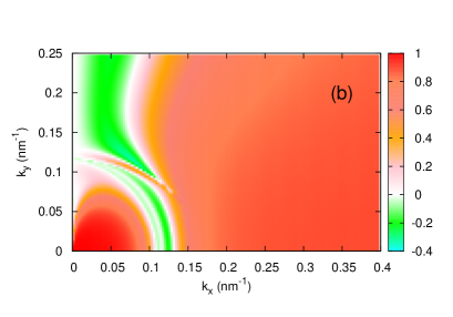
We consider the transmission of our system, which is given by the sum of the outgoing propagating components in the RS. We choose FO with magnetization along , so that in the C region we have spin-splitted bands (Y-SSB), eigenstates of , while we inject and detect in the LS and RS electron spin-polarized along . Note that as explained before, with direct gate bias, the conduction bands will be spin-splitted, while for a reverse bias the spin splitting is negligible. In Fig. 3, we show the spin differential transmission through the central region with FO deposited on the U layer, with meV and . is calculated as a function of the wavevector of the incoming particle in the LS. Fig. 3(a) is calculated with a direct potential energy difference between the graphene planes of eV. Indeed a marked resonance is observed with negative values of . Electrons of this wavevector are transmitted through the barrier with a spin rotation of . In Fig. 3(b), where eV is reversed, such a feature is absent and electrons preferentially preserve their spin orientation. The spin-transmission properties are therefore dramatically affected by changing between direct and reverse bias of the T and B gates. In particular this resonance falls into the mexican hat region of the upper Y-SSB (Fig. 2(c)), where three propagating states are active: two from the upper Y-SSB and one from the lower one. The resonance condition is given by the existence of two propagating modes, one from each of the two Y-SSBs, for which , with (here applies). In fact, an incoming particle, spin-polarized along , can be transmitted in the C region as a linear combination of two states from the two bands (eigenstates of ). These components, traveling through the C region, acquire a net phase difference of , which corresponds to a net spin-flip process. Note that the mexican hat-like dispersion makes it possible to have two propagating states with large , allowing the fulfillment of the resonance condition with as small as nm. Of course, choosing different values for leads to different positions of the spin-flip transmission resonance.
For an incoming particle of lower energy, only the lower Y-SSB contributes propagating components in the C region as shown in Fig. 2(c). The overall transmission probability has an upper limit of , because the propagating component is eigenstate of , and can be seen as a combination of half and half spin components. For the same reason, the spin differential transmission is close to zero. For an incoming particle of energy above the resonance, instead, there is one propagating component for each of the Y-SSBs (see Fig. 2(c)). However between these components is much smaller with respect to the resonance case and their phase difference accumulated by traveling through the region is negligible. Therefore both the spin differential transmission and the overall transmission are close to unity.
IV Conductance
A readily measurable property of the system is its conductance. We have therefore calculated the 2D conductance of the bilayer system with FO in the C region. In particular we are interested in the spin-flipped relative conductance , with . This is a measure of the efficiency of spin control in the proposed device. The 2D two-terminal conductance, which is defined by , is expressed as
| (14) |
with (accounting for the valley and spin degeneracy), the group velocity along the transport direction, the Fermi-Dirac distribution function and the electrochemical potential. Integration is performed over the Brillouin zone.
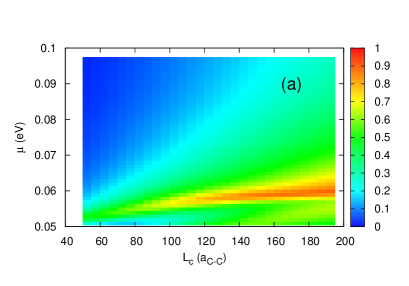
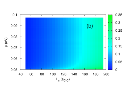
In Fig. 4 we show the spin-flip relative conductance as a function of the electrochemical potential for from to , at the temperature of K. Fig. 4(a) is computed with a direct gate bias of eV, while (b) shows the case with the reverse bias. The resonance present in (a), corresponding to an electrochemical potential for which the spin-flip affects more than of transmitted electrons, is completely absent in (b), where electrons tend to preserve their original spin. This calculation clearly demonstrates that we are able to control the spin-flip of carriers traveling through the system by changing the gate bias.
The total conductance is thermally activated as approaches the bottom of the conduction band of the LS region. As enters the 3-states spectral region in Fig. 2(c) the conductance spin properties are dominated by the behavior of the transmission probability in Fig. 3(a). This leads, with a direct bias, to a pronounced resonance of . A fundamental factor for the appearance of this resonance is that the spin differential transmission resonance in Fig. 3(a) is almost isotropic for small , similar to the LS dispersion curve, deviating only for large . Therefore, it is possible, with the appropriate electrochemical potential, to adjust the Fermi level to this transmission resonance. The states relevant to the conductance will therefore be quite well collimated on the spin-flip transmission resonance. As expected, an increase of the temperature leads to a broader state population, gradually blurring away this feature.
V Self-consistent analysis
To provide an indication of the real control that the gates exert on the system, and therefore of the observability of the phenomenon, we performed a self-consistent electrostatic analysis. Indeed, we can fix the absolute value of the chemical potential, but we cannot set the difference between the electrochemical potential and the bilayer graphene midgap. In other words, the value of the potential of the U and L layers of the graphene bilayer is the result of the self-consistent calculation, which depends on the gate voltages, taking into account the capacitive coupling with the gates. We study a double gate FET in which we can independently fix the top and back gate voltages ( and ). Alternatively we can give the average gate potential , which is responsible for rigidly shifting the bands (and therefore varying the electrochemical potential with respect to midgap), and the gate voltage difference which opens up the semiconducting gap of the graphene bilayer. To describe the electrostatics of the system we apply to the graphene bilayer the plane capacitor model described in Refs. Castro et al., 2008; Cheli et al., 2009. Another way to describe the charge on the U and L plane is band filling. In fact, the occuppation of each one of the graphene bilayer state is described by the Fermi-Dirac distribution, and the charge it carries can be distributed on the U and L plane according to and . The two descriptions of the system, electrostatics and statistics, should be consistent and their simultaneous solution fixes the U and L potentials, and therefore .
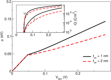
We focus our calculation on a system with eV, and analyze the control on the electrochemical potential with respect to the midgap of the graphene bilayer. In Fig. 5, we show as a function of the average gate potential , where a potential difference V and V has been applied for and nm respectively (values which lead to V). When the device is empty the electrochemical potential linearly increases with . As the electrochemical potential reaches the bottom of the conduction band, we can observe an abrupt change of slope. As the charge accumulates in the device, the variation of the electrochemical potential becomes more difficult, due to the increase of the quantum capacitance of the system Cantele et al. (1988). The spin-flip resonance region is easily reached with the tight double gate structure adopted here, which optimizes the electrostatic control. The considered oxide thicknesses are obtained with state-of-the-art semiconductor technology, and high-dielectric-constant oxides (the so called high-K dielectrics) can allow even better electrostatic control. In the inset of Fig. 5 we show the charge accumulated on the U and L plane. The charge shows an activation behavior in correspondence with the value of for which the electrochemical potential reaches the conduction band.
VI Conclusion
We have demonstrated that bilayer graphene FETs, in which a ferromagnetic insulator is used as a gate dielectric, is an interesting system for spin manipulation. In particular, we have shown that a good electric control of spin rotation can be achieved even in a 2D system without lateral confinement, at low temperature. We show that by switching between a direct and a reverse gate polarization, we can modulate the ratio of spin-flipped transmitted carriers from more than to less than . Therefore, the system itself acts as a tunable spin-flipping device and offers the possibility to devise spin-FETs based on bilayer graphene, exploiting the exchange proximity interaction with a ferromagnetic insulator, instead of the rather weak intrinsic spin-orbit coupling.
Acknowledgements.
P. M. and P. R. acknowledge financial support from the DFG via the Emmy Noether program. G. I. acknowledges financial support from the EC through the FP7 Nanosil NoE (contract n. 216171).References
- Novoselov et al. (2004) K. S. Novoselov, A. K. Geim, S. V. Morozov, D. Jiang, Y. Zhang, S. V. Dubonos, I. V. Grigorieva, and A. A. Firsov, Science 306, 666 (2004).
- Neto et al. (2009) A. C. Neto, F. Guinea, N. Peres, K. Novoselov, and A. Geim, Rev. Mod. Phys. 81, 109 (2009).
- Geim and Novoselov (2007) A. K. Geim and K. S. Novoselov, Nat. Mat. 6, 183 (2007).
- Bai et al. (2009) J. Bai, X. Duan, and Y. Huang, Nano Lett. 9, 2083 (2009).
- Seidel et al. (2005) R. V. Seidel, A. P. Graham, J. Kretz, B. Rajasekharan, G. S. Duesberg, M. Liebau, E. Unger, F. Kreupl, and W. Hoenlein, Nano Lett. 5, 147 (2005).
- Michetti et al. (2010) P. Michetti, M. Cheli, and G. Iannaccone, Appl. Phys. Lett. 96, 133508 (2010).
- Fiori and Iannaccone (2009) G. Fiori and G. Iannaccone, IEEE EDL 30, 1096 (2009).
- Cheli et al. (2009) M. Cheli, P. Michetti, and G. Iannaccone, in Proc. ESSERDC 2009 (2009), pp. 193–196.
- (9) M. Cheli, P. Michetti, and G. Iannaccone, accepted TED.
- Datta and Das (1990) S. Datta and B. Das, Appl. Phys Lett. 56, 665 (1990).
- Min et al. (2006) H. Min, J. Hill, N. Sinitsyn, B. Sahu, L. Kleinman, and A. MacDonald, Phys. Rev. B 74, 165310 (2006).
- Huertas-Hernando et al. (2006) D. Huertas-Hernando, F. Guinea, and A. Brataas, Phys. Rev. B 74, 155426 (2006).
- Tombros et al. (2007) N. Tombros, C. Jozsa, M. Popinciuc, H. T. Jonkman, and B. van Wees, Nature 448, 571 (2007).
- Jayasekera et al. (2010) T. Jayasekera, B. D. Kong, K. W. Kim, and M. Buongiorno Nardelli, Phys. Rev. Lett. 104, 146801 (2010).
- Son et al. (2006) Y.-W. Son, M. Cohen, and S. Louie, Nature 444, 347 (2006).
- Cantele et al. (2009) G. Cantele, Y.-S. Lee, D. Ninno, and N. Marzari, Nano Lett. 9, 3425 (2009).
- Žutić et al. (2004) I. Žutić, J. Fabian, and S. Das Sarma, Rev. Mod. Phys. 76, 323 (2004).
- Semenov et al. (2007) Y. Semenov, K. Kim, and J. Zavada, Appl. Phys. Lett. 91, 153105 (2007).
- Huegen et al. (2008) H. Huegen, D. Huertas-Hernando, and A. Brataas, Phys. Rev. B 77, 115406 (2008).
- Semenov et al. (2008) Y. Semenov, J. Zavada, and K. Kim, Phys. Rev. B 77, 235415 (2008).
- Dell’Anna and Martino (2009) L. Dell’Anna and A. D. Martino, Phys. Rev. B 80, 155416 (2009).
- Ohta et al. (2006) T. Ohta, A. Bostwick, T. Seyller, K. Horn, and E. Rotenberg, Science 313, 951 (2006).
- Castro et al. (2007) E. Castro, K. Novoselov, S. Morozov, N. Peres, J. L. dos Santos, J. Nilsson, F. Guinea, A. Geim, and A. C. Neto, Phys. Rev. Lett 99, 216802 (2007).
- Oostinga et al. (2008) J. Oostinga, H. Heersche, X. Liu, A. Morpurgo, and L. Vandersypen, Nature Mater. 7, 151 (2008).
- Zhang et al. (2009) Y. Zhang, T.-T. Tang, C. Girit, Z. Hao, M. C. Martin, A. Zettl, M. F. Crommie, Y. R. Shen, and F. Wang, Nature 459, 820 (2009).
- McCann (2006) E. McCann, Phys. Rev. B 74, 161403 (2006).
- Nilsson et al. (2008) J. Nilsson, A. C. Neto, F. Guinea, and N. Peres, Phys. Rev. B 78, 045405 (2008).
- Li et al. (2009) Z. Li, E. Henriksen, Z. Jiang, Z. Hao, M. Martin, P. Kim, H. Stormer, and D. Basov, Phys. Rev. Lett. 102, 037403 (2009).
- Barbier et al. (2009) M. Barbier, P. Vasilopoulos, F. Peeters, and J. P. Jr., Phys. Rev. B 79, 155402 (2009).
- Castro et al. (2008) E. Castro, N. Peres, J. L. dos Santos, F. Guinea, and A. C. Neto, Journal of Phys.: Conf. Series 129, 012002 (2008).
- Cantele et al. (1988) G. Cantele, Y.-S. Lee, D. Ninno, and N. Marzari, Appl. Phys. Lett. 52, 501 (1988).