Charged impurity scattering and mobility in gated silicon nanowires
Abstract
We study the effects of charged impurity scattering on the electronic transport properties of -oriented Si nanowires in a gate-all-around geometry, where the impurity potential is screened by the gate, gate oxide and conduction band electrons. The electronic structure of the doped nanowires is calculated with a tight-binding method and the transport properties with a Landauer-Büttiker Green functions approach and the linearized Boltzmann transport equation (LBTE) in the first Born approximation. Based on our numerical results we argue that: (1) There are large differences between Phosphorous- and Boron-doped systems, acceptors behaving as tunnel barriers for the electrons, while donors give rise to Fano resonances in the transmission. (2) As a consequence, the mobility is much larger in P- than in B-doped nanowires at low carrier density, but can be larger in B-doped nanowires at high carrier density. (3) The resistance of a single impurity is strongly dependent on its radial position in the nanowire, especially for acceptors. (4) As a result of subband structure and screening effects, the impurity-limited mobility can be larger in thin nanowires embedded in HfO2 than in bulk Si. Acceptors might, however, strongly hinder the flow of electrons in thin nanowires embedded in SiO2. (5) The perturbative LBTE largely fails to predict the correct mobilities in quantum-confined nanowires.
I Introduction
Silicon nanowires (SiNWs) have attracted significant interest as promising building blocks for nanotechnologies. They can be fabricated by bottom-up approaches Lieber03 ; PYang05 ; Thelander05 ; Schmidt10 or by techniques compatible with standard complementary metal-oxide semiconductor (CMOS) process.Pei02 ; Colinge04 ; Suk05 Recently, SiNWs with diameter below 12 nm have been manufactured with excellent structural properties, which opens new opportunities for the design of nanoscale devices and for the exploration of quantum transport phenomena in low-dimensional systems. SiNWs can be used to build gate-all-around transistors in which short channel effects are reduced thanks to a better gate control,Pei02 ; Colinge04 ; Suk05 ; Bescond04 ; Lundstrom06 and transistors based on arrays of vertically stacked SiNWs with diameter close to 10 nm have been recently reported.Bera06 ; Dupre08 ; Ng09
In this context, it is essential to understand the effects of quantum confinement on the transport properties of small SiNWs. It is well-known that the conductance would be quantized in ideal, ballistic nanowires. However, surface roughness, impurities and phonons, practically limit carrier mobilities in real devices. These scattering processes must be strongly influenced by confinement, and the physical approximations valid in bulk Si certainly break down in small enough nanowires. Recent theoretical works have therefore addressed the scattering of free carriers by phonons,Fonoberov06 ; Buin08 and by bulk and surface disorder in SiNWs.Markussen06 ; Lherbier07 ; Persson08 The scattering by dopants has also been studied with either density functional theory (DFT) Fernandez06 ; Fernandez06b ; Markussen07 ; Rurali08 or the semi-empirical effective mass Jin07 ; Oh08 ; Martinez09 ; Bescond09 ; Bescond10 approximation. Most DFT calculations reported so far Fernandez06 ; Fernandez06b ; Markussen07 have, however, considered neutral dopants. Indeed, the treatment of charged dopants within DFT is more problematic, because of the long range character of the Coulomb impurity potential, and because of intrinsic deficiencies in the present exchange-correlation functionals.Niquet10 The influence of a charged dopant on the transmission through a 2 nm diameter SiNW has nonetheless been discussed recently with DFT in Ref. Rurali08, . This work showed, in particular, that minority carriers are blocked by the impurities, but did not consider screening by the environment or free carriers, which is known to be essential from bulkConwell50 ; Sanborn92 , to nanowires.Jin07 There is, therefore, a clear need for a better assessment of the effects of impurities in nanowires with more realistic potentials.
In this work, we study the scattering of electrons by charged donor (phosphorous) and acceptor (boron) impurities in SiNWs. The scattering of electrons by acceptors occurs for example in -doped transistor channels in the inversion regime. The Coulomb potential of an impurity in a nanowire is strongly dependent on its dielectric environment. In (small) free-standing nanowires, the Coulomb potential is indeed almost unscreened due to the presence of surface polarization charges in the vicinity of the impurity. Consequently, the binding energy of the dopants is much enhanced with respect to the bulk (it increases as ), which leads to a significant decrease of the doping efficiency in small ( nm) nanowires.Diarra07 ; Diarra08 ; Li08 ; Bjork09 ; Yoon09 In the following, we consider SiNWs surrounded by an oxide layer and a metallic gate, i.e. a gate-all-around geometry typical of nanowire devices. In this case the impurity potential is efficiently screened by the gate, the binding energy remains close to its bulk value, and most of the donor impurities are ionized at room temperature (acceptors being usually charged negatively in the inversion regime).Diarra07 ; Diarra08
Only a few theoretical works have addressed the effect of charged impurities on the transport in gated SiNWs, with either the (perturbative) Kubo-Greenwood formulaJin07 or a (non-perturbative) Green function approach,Oh08 ; Martinez09 ; Bescond09 ; Bescond10 but using the effective mass approximation for the electronic structure. Our objective is to go beyond these approximations and to perform a systematic study as function of the type of impurity (donor or acceptor), its radial position in the wire, the diameter of the SiNWs and the nature of the oxide. For that purpose, we combine a tight-binding method for the electronic structure with a Landauer-Büttiker (LB) Green functions approach for transport. We take into account the screening of the impurity potential by the oxide, gate, and free electrons. We use the low-field mobility as a metric of the scattering strength of the impurities, which we calculate from the resistances of a representative set of single impurities. We compare Green functions with the linearized Boltzmann transport equation (LBTE) in the first Born approximation, where the impurity is treated as a perturbation.
The paper is organized as follows: We first review the methodology in section II, then evidence the main trends and conclusions in the particular case of a 2 nm thick HfO2 gate oxide in section III. We last discuss other gate oxides and thicknesses in section IV, and summarize our conclusions in section V.
II Methodology
We consider cylindrical hydrogen-passivated SiNWs oriented along the direction. The electronic structure of the nanowires is calculated with an accurate TB parametrizationBoykin04 previously validated by ab initio calculations and comparison with experimental data.Niquet06 Each impurity is modeled by a hydrogenic potential screened by the dielectric environment, as discussed in Refs. Diarra07, and Diarra08, . We assume in this respect that the SiNWs are surrounded by a conformal layer of SiO2 or HfO2 with thickness and a metallic gate (gate-all-around geometry). Image charge self-energy effects are included along the lines of Refs. Diarra08, and Niquet06, .
The impurity potential can also be screened by the free electrons. To account for that mechanism, we first compute the self-consistent conduction band wave functions of the homogeneous nanowire at the target carrier density . We then calculate the density-density response function of the conduction band electrons with these wave functions, and solve Poisson’s equation for the screened impurity potential in the linear-response approximation. This is equivalent to the so-called Random Phase Approximation (RPA) for the free carriers.Delerue05 We finally compute the impurity resistance with the Green functions approach and LBTE.
In the non-perturbative Landauer-Büttiker approach,Landauer57 the SiNWs are coupled to ideal semi-infinite leads and the total transmission probability is computed as a function of the electron energy from the Green function, which is evaluated with a standard decimation techniqueLherbier07 ; Grosso89 or a newly implemented “knitting” algorithmKazymyrenko08 (for diameters nm). We consider sufficiently diluted systems and/or a generic source of incoherence (e.g., phonons) so that interference effects induced by multiple scattering events involving more than one impurity can be neglected. The resistance of a single impurityMarkussen07 is then , where () is the conductance of the nanowire with (without) impurity at temperature and chemical potential . Both and are given by the finite temperature Landauer-Büttiker formula:
| (1) |
where is the quantum of conductance (assuming spin degeneracy) and is the Fermi-Dirac distribution function. We will see in the following that the resistance of an impurity strongly depends on its radial position in the nanowire. We therefore define a mean resistance averaged over a set of at least 16 impurity positions, from which we deduce the conductivity
| (2) |
and the mobility (where is the free carrier density, and the impurity concentration).
We also compute the mobility of the SiNWs within the LBTE in the first Born approximation, treating the impurity potential as a perturbation. This approach has been widely used to calculate the carrier mobility in various materials (see for example Ref. Conwell50, for bulk Si). The relaxation time of an electron with wavevector in subband and energy fulfills the following set of equations:
| (3) | |||||
where is the length of the wire, is the group velocity, spans all subbands, and is a square matrix element of the impurity potential . These matrix elements are computed with the unperturbed TB wave functions .Diarra07 ; Diarra08 The resistance of the impurity is then given by:
| (4) |
The average impurity resistance and mobility are finally defined as in the Landauer-Büttiker approach.
III Case study: 2 nm thick HfO2 gate oxide
In this section, we evidence the main trends and conclusions on gate-all-around SiNWs with a 2 nm thick HfO2 gate oxide. We first discuss the main features of the transmission, then the size dependence of the electron mobility, some variability issues and the screening by free carriers.
III.1 Transmission
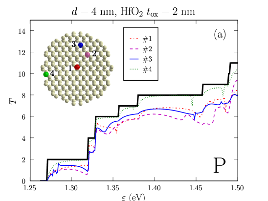
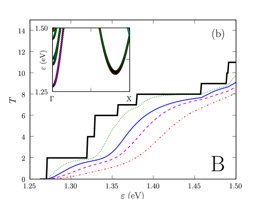
Figure 1 shows the total Landauer-Büttiker transmission as a function of energy, calculated for phosphorous (P) and boron (B) impurities in a 4 nm diameter SiNW. The carrier density is assumed to be low enough ( cm-3, see later discussion) so that screening by free electrons can be neglected. In the absence of impurity is equal to the number of open channels (subbands) at energy ; the onset of transport through a new subband gives rise (at zero temperature) to a plateau in the conductance as a function of gate voltage. In the presence of a charged P or B dopant, the transmission is reduced due to the scattering of the electrons by the impurity potential.
Two important effectsFernandez06 ; Markussen07 are clearly visible in Fig. 1: (i) The scattering strength strongly depends on the position of the impurity in the SiNW; (ii) The transmission behaves very differently for donors and acceptors. Indeed, the donor potential (Fig. 1a) is a quantum well whose (quasi-)bound states give rise to Fano resonances, which appear as asymmetric dips and peaks in the transmission. They are typical of quantum-confined waveguides and result from the interference of the carrier wave function with the quasi-bound states of the higher-lying subbands.Tekman93 ; Kim99 ; Vargiamidis05 The number, position and width of these Fano resonances depends on the position of the impurity in the SiNW. Although they are mostly washed-out by thermal broadening at room temperature, the Fano resonances have subtle effects on the mobility, as discussed below. On the other hand acceptors behave as tunnel barriers which give rise to the smoother, resonance-free transmission curves of Fig. 1b. The transmission is, on average, significantly smaller for B than for P impurities at low carrier density, in agreement with the above-given physical picture. The transmission in gate-all-around, B-doped nanowires remains, however, orders of magnitude larger than in free-standing SiNWs in vacuum (see Ref. Rurali08, ), where the impurity is completely unscreened.noteunscreened
III.2 Mobility
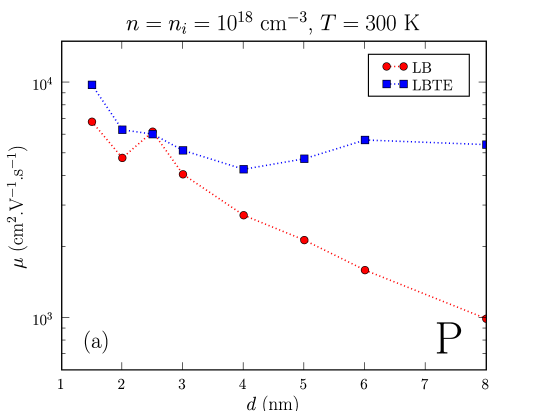
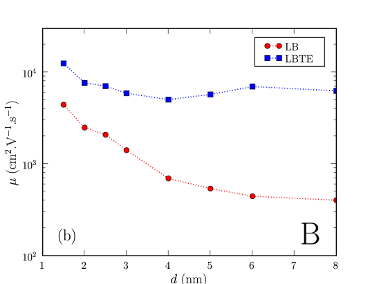
The electron mobility calculated with the LB and LBTE approaches is plotted in Fig. 2 as a function of the SiNW diameter, for both donors and acceptors ( cm-3). As expected, the Landauer-Büttiker mobility in B-doped SiNWs (inversion regime) is smaller than in P-doped SiNWs because the acceptor potential acts as a barrier for the electrons. In contrast, the LBTE mobilities are – almostnote1 – identical for P and B since the coefficients do not depend on the sign of the impurity potential (they are ), a serious weakness of the first Born approximation. There is an order-of-magnitude difference between the two approaches for acceptors, and at best an order-of-magnitude agreement for donors. The error made by the LBTE is larger for acceptors because the electrons can hardly go around the barrier raised by the impurity in a nanowire, a very unfavorable situation for a perturbative approach. Although neither bound nor quasibound states can be addressed by perturbation theory, thermal broadening often helps for donors. Overall, the LBTE in the first Born approximation does not appear to be reliable enough for the prediction of impurity-limited mobilities in SiNWs, even when the potential is shorter ranged than in bulk as in gate-all-around devices.
For the HfO2 gate oxide, the Landauer-Büttiker mobility mostly increases with decreasing wire diameter at given carrier density and impurity concentration . This trend might appear counter-intuitive, as confinement is expected to strengthen the interaction of the carriers with the impurities. It can be explained by a combination of three factors: First, the impurities are more efficiently screened by the gate and gate oxide in small SiNWs. This is especially sensitive for acceptors, because screening reduces the height and width of the barrier the electrons have to go through. Second, confinement increases the separation between conduction subbands, which reduces the number of channels available for inter-subband scattering (see the inset of Fig. 1b). Third, confinement also lifts the sixfold valley degeneracy of bulk Si, and splits the ground-state, twofoldnotevalley degenerate valleys at from the higher-lying, fourfoldnotevalley degenerate valleys at .Niquet06 The valleys therefore progressively empty with decreasing diameter, in favor of the valleys. This enhances the mobility because the valleys feature a lower transport mass than the valleys.Persson08 In this respect, we would like to point out that inter-valley scattering does not significantly limit the mobility, because the range of the impurity potential, although screened by the gate and conduction band electrons, is still much larger than the unit cell (large wave vectors – and thus very short-range potentials – are indeed required to transfer an electron between the and valleys). The small fluctuations of the mobility around the main trend visible in Fig. 2 are due to band structure and Fano resonance effects.
The mobility in B-doped SiNWs tends to level slightly below cm2.V-1.s-1 in the largest nanowires investigated in this study, while the mobility in P-doped SiNWs still shows a significant slope but bends upwards. The experimental room-temperature mobility in bulk, P- and As- doped silicon is cm2.V-1.s-1 at cm-3, and cm2.V-1.s-1 at low carrier density (phonon-limited mobility).Masetti83 Assuming that Matthiessen’s rule holds and that the phonon-limited mobility is weakly dependent on the carrier density, the impurity-limited mobility in bulk -type Si would therefore be cm2.V-1.s-1 at cm-3. More refined treatmentsSanborn92 ; Mole99 suggest a larger cm2.V-1.s-1. The mobility of minority electrons in -type Si is, of course, much less known but appears to be in the same range.Swirhun86 These data imply that (i) the impurity-limited mobility can be larger in thin gate-all-around devices than in bulk silicon, and (ii) that the impurity-limited mobility in B-doped SiNWs embedded in HfO2 might exhibit a shallow minimum in the nm range. We will further discuss these issues for different gate oxides and thicknesses in section IV.
III.3 Variability
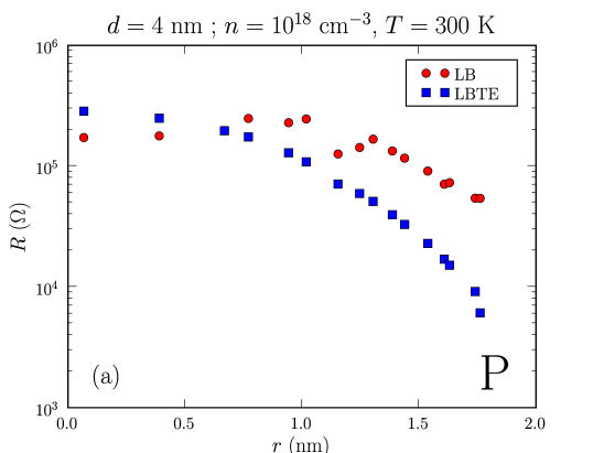
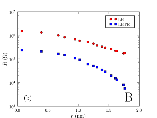
The resistance of single impurities in a 4 nm diameter SiNW is plotted as a function of their radial coordinate in Fig. 3, in both the LB and LBTE approaches ( cm-3). As expected from Fig. 1, the resistance of an impurity is strongly dependent on its radial position in the nanowire (the angular dependence being much weaker). It tends to decrease close to the surface as the impurity moves out of the main flow of electrons and is better screened by the gate. While the random fluctuation of the number of dopants in ultimate transistors is already considered as a major issue in the microelectronics industry,Kuhn08 our results show that the fluctuation of the impurity positions also contributes to the variability in thin SiNW transistors. The resistance of single B impurities is monotonously decreasing from the center to the surface of the SiNW. It spans around one order of magnitude (for diameters nm), due to the sensitivity of the tunneling current to the barrier height and width. The resistance of single P impurities is more weakly dependent on their radial position and might be non-monotonous. For example, the sharp feature around nm in Fig. 3a coincides with a rapid change in the distribution of Fano resonances in the first subband [see the magenta (#2) and blue (#3) curves in Fig. 1]. For both P and B, the difference between the LB and LBTE resistances is maximum at the surface, because the matrix elements of the potential, , decrease too fast in the first Born approximation when the impurity moves out of the electron flow.
III.4 Screening by free carriers
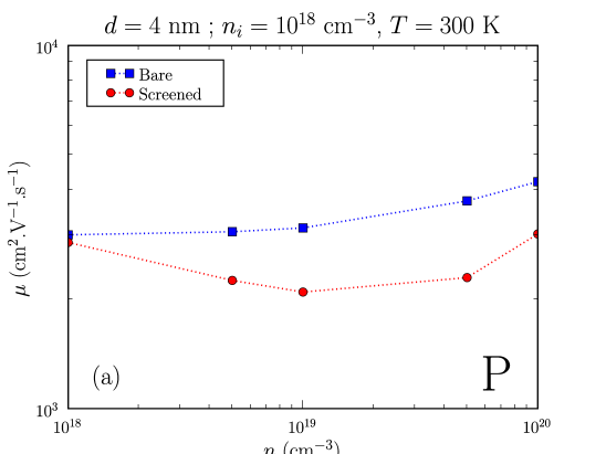
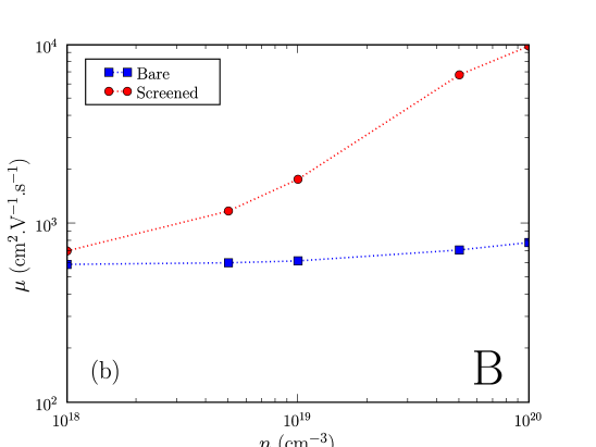
In practice, the carrier density can be modulated by the gate voltage. The Landauer-Büttiker mobility in a 4 nm diameter SiNW is plotted as a function of in Fig. 4, for both donors and acceptors with a concentration cm-3. The “bare” data does not take screening by the free electrons into account, while the “screened” data does. The trends evidenced in Fig. 4 are typical of the investigated diameter range.
At room temperature, the bare mobility is essentially constant in the whole cm-3 range, which shows that mobility is a relevant concept in long channels down to the smallest SiNWs. The bare and screened mobilities almost coincide at low carrier densities cm-3 where the impurities are mainly screened by the gate and gate oxide only. As the electron density is further increased, the free carriers effectively reduce the range and depth of the impurity potential. This strongly enhances, as expected, the mobility in B-doped SiNWs (by around one order of magnitude at cm-3). The mobility in P-doped nanowires remains, however, almost constant up to cm-3. It even features a shallow minimum around cm-3, which means that the conductivity increases sub-linearly with carrier density. This counter-intuitive trend results from the interplay between the impurity well and lateral quantum confinement, and from the complex behavior of Fano resonances. Indeed, as shown for example in Figs. 1 and 2 and in the appendix of Ref. Vargiamidis05, , the decrease of the depth (or width) of a well placed along a quantum-confined electron waveguide does not necessarily improve the background transmission through this waveguide. In addition, the Fano resonances of the first subband are pushed closer the edge of the second subband as the range of the potential decreases, which markdely affects the transmission profile around the Fermi energy. As a consequence, the mobility in B-doped nanowires can be larger than the mobility in P-doped nanowires at “high” carrier density cm-3. This again shows that screening – either by the dielectric environment or by the free carriers – can not be neglected when discussing the transport properties of SiNWs in the inversion regime.
IV Role of the gate oxide
In this section, we discuss the mobility in P- and B- doped SiNWs with different gate oxides and thicknesses.
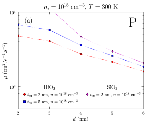
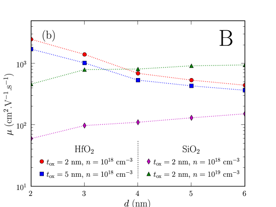
The room-temperature mobility in P- and B- doped SiNWs is plotted as a function of the nanowire diameter in Fig. 5, for a 2 nm and a 5 nm thick HfO2 gate oxide, as well as for a 2 nm thick SiO2 gate oxide. The impurity concentration is cm-3; The carrier density is cm-3 or cm-3. The impurity potentials are more shallow in HfO2 than in SiO2 (due to the larger dielectric constant), but get even shorter-ranged when the thickness of the oxide decreases (the range of the potential is, indeed, roughly proportional to the gate radius at low carrier densities).
The mobility in SiNWs embedded in HfO2 is weakly dependent on the oxide thickness. Indeed, a few nanometers of such a high- material are enough to screen the impurities almost completely, so that the effect of the gate becomes insignificant. Still, as expected, the mobility in B-doped SiNWs increases when decreasing the oxide thickness. However, the mobility in P-doped SiNWs slightly decreases with decreasing , again showing that a better screening does not necessarily come with an enhancement of the mobility in P-doped quantum-confined nanowires.
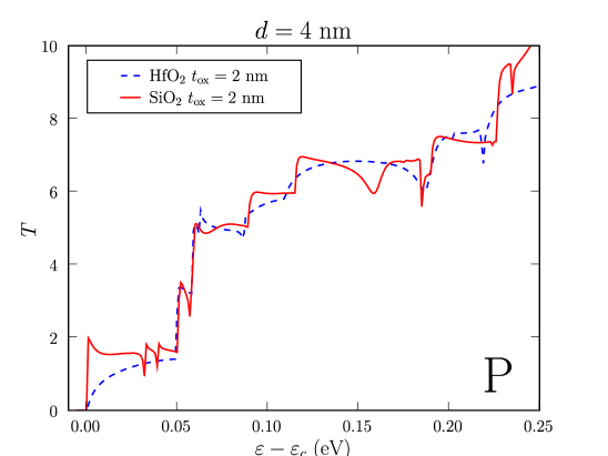
This is further evidenced by the SiO2 data. Again, the mobility in P-doped SiNWs increases (with respect to HfO2) despite the lower dielectric constant. The potential landscape around the impurity is indeed very different in SiO2 and HfO2 (see later discussion for B impurities), which leads to different background transmission profiles and Fano resonances. This is illustrated in Fig. 6 for a 4 nm diameter SiNW: while the transmission is small around the conduction band edge in HfO2, it is finite in SiO2, and shows more and stronger resonances in the first subbband. Still, the difference between SiO2- and HfO2-coated P-doped SiNWs decreases with increasing nanowire diameter as quantum confinement gets weaker and the transport becomes multi-band.
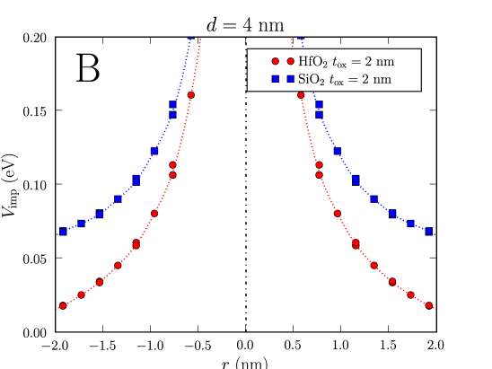
The mobility in B-doped SiNWs embedded in SiO2 is strongly hindered at low carrier densities. At variance with all previous cases, it increases with increasing nanowire diameter. The mobility in these nanowires is actually limited by the lateral extension of the barrier raised by the acceptor. This is illustrated in Fig. 7, which represents the potential of a B impurity in the cross section of a 4 nm diameter nanowire. In HfO2, the impurity potential is almost zero already at the surface of the nanowire, allowing for significant transmission even at low carrier energy. In SiO2, the potential is still sizeable at the surface of the nanowire, effectively preventing the flow of carriers throughout the whole cross section over meV above the conduction band edge, and quenching the mobility. As the nanowire diameter increases, the height of this residual barrier decreases (because there is more space around the impurity for the potential to decay), and the mobility increases. Also, this barrier can be significantly lowered by the free carriers, as evidenced by the cm-3 data in Fig. 5. Although this might increase the ratio of B-doped channels embedded in SiO2, we conclude from these results that the introduction of high- oxides is mandatory in ultimate nanowire devices to prevent strong impurity scattering.
V Conclusions
In conclusion, the effects of charged (P and B) impurities on the electron transport properties of -oriented gate-all-around SiNWs with diameters nm have been analyzed using the Landauer-Büttiker approach and the linearized Boltzmann transport equation (LBTE). The main results of our calculations are:
(1) Whereas the transmission in B-doped SiNWs presents a monotonous dependence on energy, the transmission in P-doped SiNWs shows a complex behavior with multiple Fano resonances.
(2) At low carrier density, the mobility is much larger in P-doped nanowires in accumulation than in B-doped nanowires in inversion.
(3) The resistance of single impurities (especially acceptors) strongly depends on their radial position in the nanowire, which may represent an important source of variability in ultimate transistors based on SiNWs.
(4) The mobility in P-doped quantum confined SiNWs does not necessarily increase when the impurities are better screened. In particular, the mobility is weakly dependent on the carrier density in P-doped SiNWs embedded in HfO2, while it rapidly increases with carrier density in B-doped SiNWs. As a consequence, the mobility can be larger in B- than in P-doped SiNWs at high carrier density.
(5) In SiNWs embedded in HfO2, the impurity-limited mobility increases with decreasing wire diameter, and can be larger in the smallest nanowires than in bulk Si. On the opposite, acceptors might severely quench the mobility in B-doped SiNWs embedded in SiO2. The use of high- gate oxides is therefore mandatory in ultimate SiNW devices to prevent strong impurity scattering.
(6) The error made by the perturbative LBTE with respect to the Landauer-Büttiker approach is usually very large in quantum-confined nanowires.
Acknowledgements
This work was supported by the EU Project No. 015783 NODE, by the French National Research Agency (ANR) projects PREEANS and QUANTAMONDE. The calculations were performed at the CCRT and CINES supercomputing centers.
References
- (1) C. M. Lieber, Mater. Res. Soc. Bull. 28, 486 (2003).
- (2) P. Yang, Mater. Res. Soc. Bull. 30, 85 (2005).
- (3) C. Thelander, H. A. Nilsson, L. E. Jensen, and L. Samuelson, Nano Lett. 5, 635 (2005).
- (4) V. Schmidt, J. V. Wittemann, and U. Gösele, Chem. Rev. 110, 361 (2010).
- (5) G. Pei, J. Kedsierski, P. Oldiges, M. Ieong, and E. C. C. Kan, IEEE Trans. Electron Devices 49, 1411 (2002).
- (6) P. Colinge, Solid-State Electron. 48, 897 (2004).
- (7) S. D. Suk, S.-Y. Lee, S.-M. Kim, E.-J. Yoon, M.-S. Kim, M. Li, C. W. Oh, K. H. Yeo, S. H. Kim, D.-S. Shin, K.-H. Lee, H. S. Park, J. N. Han, C. J. Park, J.-B. Park, D.-W. Kim, D. Park, and B.-I. Ryu, IEDM Tech. Digest 2005, 717 (2005).
- (8) M. Bescond, J. L. Autran, D. Munteanu, and M. Lannoo, Solid-State Electron. 48, 567 (2004).
- (9) M. Lundstrom and J. Guo, Nanoscale Transistors: Device Physics, Modeling and Simulation (Springer, 2006).
- (10) L. K. Bera, H. S. Nguyen, N. Singh, T. Y. Liow, D. X. Huang, K. M. Hoe, C. H. Tung, W. W. Fang, S. C. Rustagi, Y. Jiang, G. Q. Lo, N. Balasubramanian, and D. L. Kwong, IEDM Tech. Digest 2006, 551 (2006).
- (11) C. Dupré, A. Hubert, S. Bécu, M. Jublot, V. Maffini-Alvaro, C. Vizioz, F. Aussenac, C. Arvet, S. Barnola, J.-M. Hartmann, G. Garnier, F. Allain, J.-P. Colonna, M. Rivoire, L. Baud, S. Pauliac, V. Loup, P. Rivallin, B. Guillaumot, G. Ghibaudo, O. Faynot, T. Ernst, and S. Deleonibus, IEDM Tech. Digest 2008, 749 (2008).
- (12) R. M. Y. Ng, T. Wang, F. Liu, X. Zuo, J. He, and M. Chan, IEEE Electron Device Lett. 30, 520 (2009).
- (13) V. A. Fonoberov and A. A. Balandin, Nano Lett. 6, 2442 (2006).
- (14) K. Buin, A. Verma, A. Svizhenko, and M. P. Anantram, Nano Lett. 8, 760 (2008).
- (15) T. Markussen, R. Rurali, M. Brandbyge, and A.-P. Jauho, Phys. Rev. B 74, 245313 (2006).
- (16) A. Lherbier, M. P. Persson, Y. M. Niquet, F. Triozon, and S. Roche, Phys. Rev. B 77, 085301 (2008).
- (17) M. P. Persson, A. Lherbier, Y. M. Niquet, F. Triozon, and S. Roche, Nano Letters 8, 4146 (2008).
- (18) M. V. Fernández-Serra, Ch. Adessi, and X. Blase, Nano Lett. 6, 2674 (2006).
- (19) M. V. Fernández-Serra, Ch. Adessi, and X. Blase, Phys. Rev. Lett. 96, 166805 (2006).
- (20) T. Markussen, R. Rurali, A.-P. Jauho, and M. Brandbyge, Phys. Rev. Lett. 99, 076803 (2007).
- (21) R. Rurali, T. Markussen, M. Brandbyge, and A.-P. Jauho, Nano Lett. 8, 2825 (2008).
- (22) S. Jin, M. V. Fischetti, and T.-W. Tang, J. Appl. Phys. 102, 083715 (2007).
- (23) J. H. Oh, D. Ahn, Y. S. Yu, and S. W. Hwang, Phys. Rev. B 77, 035313 (2008).
- (24) A. Martinez, A. R. Brown, N. Seoane, and A. Asenov, Journal of Physics: Conference Series 193, 012047 (2009).
- (25) M. Bescond, M. Lannoo, F. Michelini, L. Raymond, and M. G. Pala, Microelectronics Journal 40, 756 (2009).
- (26) M. Bescond, M. Lannoo, L. Raymond and F. Michelini, J. Appl. Phys. 107, 093703 (2010).
- (27) Y. M. Niquet, L. Genovese, C. Delerue and T. Deutsch, Phys. Rev. B 81, 161301(R) (2010)
- (28) E. M. Conwell and V. F. Weisskopf, Phys. Rev. 77, 388 (1950); H. Brooks and C. Herring, Phys. Rev. 83, 879 (1951).
- (29) B. A. Sanborn, P. B. Allen, and G. D. Mahan, Phys. Rev. B 46, 15123 (1992).
- (30) M. Diarra, Y. M. Niquet, C. Delerue, and G. Allan, Phys. Rev. B 75, 045301 (2007).
- (31) M. Diarra, C. Delerue, Y. M. Niquet, and G. Allan, J. Appl. Phys. 103, 073703 (2008).
- (32) B. Li, A. F. Slachmuylders, B. Partoens, W. Magnus, and F. M. Peeters, Phys. Rev. B 77, 115335 (2008).
- (33) M. T. Björk, H. Schmid, J. Knoch, H. Riel, and W. Riess, Nature Nanotechnology 4, 103 (2009).
- (34) J. Yoon, A. M. Girgis, I. Shalish, L. R. Ram-Mohan, and V. Narayanamurti, Appl. Phys. Lett. 94, 142102 (2009).
- (35) T. B. Boykin, G. Klimeck, and F. Oyafuso, Phys. Rev. B 69, 115201 (2004).
- (36) Y. M. Niquet, A. Lherbier, N. H. Quang, M. V. Fernández-Serra, X. Blase, and C. Delerue, Phys. Rev. B 73, 165319 (2006).
- (37) C. Delerue and M. Lannoo, Nanostructures: Theory and Modelling (Springer, 2004).
- (38) R. Landauer, IBM J. Res. Dev. 1, 223 (1957); M. Büttiker and R. Landauer, Phys. Rev. Lett. 49, 1739 (1982).
- (39) G. Grosso, S. Moroni, and G. P Parravicini, Phys. Rev. B 40, 12328 (1989).
- (40) K. Kazymyrenko and X. Waintal, Phys. Rev. B 77, 115119 (2008).
- (41) E. Tekman and P. F. Bagwell, Phys. Rev. B 48, 2553 (1993).
- (42) C. S. Kim, A. M. Satanin, Y. S. Joe and R. M. Cosby, Phys. Rev. B 60, 10962 (1999).
- (43) V. Vargiamidis and H. M. Polatoglou, Phys. Rev. B 72, 195333 (2005).
- (44) We do, indeed, get the same results as in Ref. Rurali08, for unscreened impurities: The transmission of minority carriers is blocked over a few hundreds of meV around the band edges. However, the transport of minority carriers mostly happen in gated devices, so that the impurities are, in practice, screened by oxides, gates and free carriers.
- (45) The Coulomb potentials for P and B are not exactly equal in absolute value because they differ on the impurity site, corresponding to different chemical shifts.Diarra07 ; Diarra08
- (46) The and valleys are exactly two- and fourfold degenerate in the effective mass approximation only. In the tight-binding approach, intervalley couplings completely lift the degeneracies within the and valleys. This is for example visible in Fig. 1: The two steps around eV actually correspond to the valleys.
- (47) G. Masetti, M. Severi, and S. Solmi, IEEE Trans. Dev. Electron Dev. 30, 764 (1983).
- (48) P. J. Mole, J. M. Rorison, J. A. del Alamo and D. Lancefield, in Properties of Crystalline Silicon, ed. by Robert Hull (INSPEC, 1999).
- (49) S. E. Swirhun, Y. H. Kwark, and R. M. Swanson, IEDM Technical Digest 1986, 27 (1986).
- (50) K. J. Kuhn, C. Kenyon, A. Kornfeld, M. Liu, A. Maheshwari, W.-K. Shih, S. Sivakumar, G. Taylor, P. VanDerVoorn, and K. Zawadzki, Intel Technology Journal 12, 93 (2008).