Strain effect on quantum conductance of graphene nanoribbons from maximally localized Wannier functions
Abstract
Density functional study of strain effects on the electronic band structure and transport properties of the graphene nanoribbons (GNR) is presented. We apply a uniaxial strain () in the (nearest-neighbor) and (second nearest-neighbor) directions, related to the deformation of zigzag and armchair edge GNRs (AGNR and ZGNR), respectively. We calculate the quantum conductance and band structures of the GNR using the Wannier function in a strain range from to (minus and plus signs show compression and tensile strain). As strain increases, depending on the AGNR family type, the electrical conductivity changes from an insulator to a conductor. This is accompanied by a variation in the electron and hole effective masses. The compression in ZGNR shifts some bands to below the Fermi level () and the quantum conductance does not change, but the tensile causes an increase in the quantum conductance to near the . For transverse direction, it is very sensitive to strain and the tensile causes an increase in the conductance while the compressive decreases the conductance at first but increases later.
pacs:
71.70.Fk, 72.80.Rj, 73.61.WpI Introduction
The discovery of graphene in 2004 and its potential application in nanotechnology has attracted considerable interest Neto et al. (2009); Reina et al. (2009); Kim et al. (2009). The unique properties of graphene due to massless Dirac fermions, high surface to volume ratio, high crystal quality in 2D, and high mechanical strength recommend it as a promising material for technologies such as nanoelectromechanical systems (NEMS) and nanosensors Geim and Novoselov (2007); Novoselov et al. (2004, 2005, 2006). Use of graphene in nanodevices is accompanied by induced strains and stresses. These may originate from phonon-induced lattice vibrations, lattice mismatched film growth, or applied external stress, and it is therefore necessary to take them into account.
Recently, research has focused on strained graphene in order to study the effect of strain on the electronic structure properties Cadelano et al. (2009); Pereira et al. (2009); Pereira and Castro Neto (2009); Farjam and Rafii-Tabar (2009). Deformations in a graphene sheet affect its electron transport by decreasing its conductance at low densities, making electrons behave in the same way as in a nanoribbon or a quantum dot Pereira and Castro Neto (2009). Theoretical studies of the strain effects, followed by recent experiments, have attempted to understand and control the interplay between the strain and the electrical transport in graphene Kim et al. (2009); Bao et al. (2009).
In a nanoribbon, the wave function is localized in two dimensions. Because of the finite size of a GNR, Bloch orbitals cannot be used directly in electronic transport calculations, and quantum conductance should be computed via lattice Green’s function and localized orbital representation of the electronic states in real space. Here, we employ maximally localized Wannier functions (MLWF) to compute the electrical conduction properties Souza et al. (2001).
In this paper we perform an study of the strain effect on a flat GNR as the structural motif for carbon nanotubes, and other graphene-based materials Saito et al. (1998). We calculate the coherent transport properties of nanostructures from first principles by combining them with the Landauer approach Nardelli et al. (2001). The connection between first principles and Landauer approach is provided by using MLWF representation. Using MLWFs, we calculate the band structure and the quantum conductance of a GNR under various strains. The results show that the transport properties of a GNR depend on the strain. As the strain increases, depending on the AGNR family type, the electrical conductivity changes from an insulator to a conductor, and this is accompanied by a variation in the electron and hole effective masses. The compression in the ZGNR shifts some bands to below the and the quantum conductance does not change, but the tensile causes an increase in the quantum conductance to near the . For transverse direction, the ZGNR is very sensitive to the strain, and the tensile causes an increase in the conductance while the compressive decreases it at first, but increases later.
II computational details
First-principles DFT-based calculations, which have been successfully applied to the study of graphene Leenaerts et al. (2008), have been performed in this paper. All our DFT calculations were carried out with the PWSCF code Baroni et al. ; Giannozzi et al. (2009), within the local density approximation (LDA) and using the ultrasoft Rabe-Rappe-Kaxiras-Joannopoulos pseudopotentials Rappe et al. (1990). We use an MLWF basis set which can be obtained by a unitary transformation of the occupied ground-state plane wave eigenfunctions of the density functional theory with the cutoff energy of 340 eV. The total system consists of 12 and 18 C atoms (graphene supercell) in a slab geometry in two dimensions (Fig. 1) and with a distance of 14 Å between the adjacent layers. The sampling of the Brillouin zone is done using a Monkhorst-Pack grid Monkhorst and Pack (1976), which is tested to give converged results for all properties that are calculated. MLWFs are computed following the method of Marzari and Vanderbilt (MV) using code Marzari and Vanderbilt (1997); Mostofi et al. (2008). For entangled energy bands, the method of Souza, Marzari and Vanderbilt (SMV) is used Souza et al. (2001). The coordinate optimization is done via conjugate gradient molecular dynamics with geometry constrains in induced strain direction, and the maximum atomic displacement is limited to 0.1 Å for each molecular dynamics step in order to preserve the stability of calculations.
III results and discussion
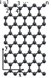
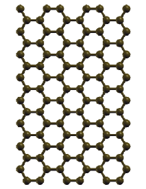
The structure studied in this work is made from a graphene sheet that is sheared along a zigzag or an armchair edges and passivated by hydrogen atoms (Fig. 1). Recently, the effects of edge and size on the GNR band structures and also the effect of charge transfer from substrate to a graphene layer have been studied Varchon et al. (2007); Finkenstadt et al. (2007). Here, we have neglected the charge transfer from substrate, and the edge and size effects, and have only considered the strain effects. We represent the deformation of the GNR by the strain () defined as where is the strain induced superlattice constant in the directions. To study the strain effects, we consider the longitudinal and transverse strains separately i.e., in the and directions.
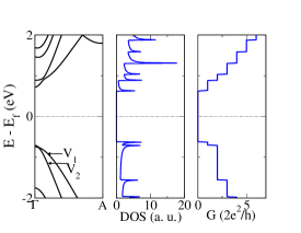
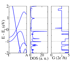
First we calculate the electronic structure of the AGNR at zero strain. An AGNR with widths = 9, 10, and 11 is chosen to represent three typical families corresponding to 3, 3+1, and 3+2 (Fig. 1), respectively, similar to the previous works Son et al. (2006); Wang et al. (2007). We present every family with key as -AGNR. Fig. 2 presents the band structures, the density of states and the quantum conductance of a 9-AGNR. Neglecting the edge effects, due to passivation, bonds, that create band dispersion in out of the basal plane, are responsible for band mixing. The band structure is spanned by the bonding combination of orbitals (the graphitic backbone) and orbitals ( and bands). The hopping integral of the bands dispersion near the determines the band gap, the transport property, and the effective mass of the charge carrier. As shown in Fig. 2, at point, there is a direct gap of 1.4 eV between the valence and conduction bands. In the valence band, the heavy hole band ( subband) is separated from the light hole band ( subband). Van Hove singularity in the density of states shows this band splitting.
Using retarded and advanced Green’s functions, based on the Landauer formalism, quantum conductance is computed. MLWFs, evaluated by a combination of plane-wave electronic structure, is applied for further conductance calculation. To construct the wave functions we select an energy window with eV around the (taken as the reference zero). This energy window contains all the occupied and empty states. Fig. 2 shows the quantum transport of the 9-AGNR and its value near the is zero. Here, conductance includes sum over all transmission possibilities that are between 0 and 1. Therefore, there are no channels to connect the two sides of the 9-AGNR near the .
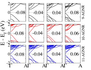
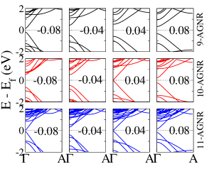
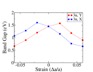
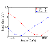
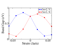
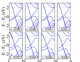
Fig. 3 shows the band structures of three families of AGNR under various uniaxial tensile () and compressive () strains. The band structures of the AGNR families are sensitive to the strain, and the band gap changes non-symmetrically for the tensile and the compressive strains as shown in Fig.4. For the 3 family in Fig.4(a) the tensile and the compressive increase the band gap at first and then reach a maximum value at a strain of about and , and finally the application of further strain decreases the band gap. Band gap variation for the 3+1 group is shown in Fig. 4(b). It suppressed to a narrow gap when the induced strain reaches and , while the compressive strain in direction and the tensile strain in direction increase the band gap to above 1 eV. Band gap variation for the 3+2 family is completely different, and has a maximum and a minimum (Fig. 4(c)). The tensile decreases the gap, while the compressive strain causes it to increase the gap. The corresponding maximum gap occurs at and and the minimum is at and . As shown in Fig. 4, all the behavior in the direction is inverse of that in the direction, and our results demonstrate that the band gap does not vanish under any condition.
Another result from Fig. 3(a) and 3(b) is the variation in the effective mass of fermions as the strain induced curvature of bands at point, that is related to the effective mass, changes. When the tensile strain becomes compressive, in addition to variation in the effective mass, the heavy hole band near the band edge ( subband) exchanges with the light hole band ( subband). The variation in the effective mass is different for =9 and 10, 11. The deformation of the 9-AGNR only causes a variation in the effective mass, but for the 10 and 11-AGNR family it can decrease the fermion’s effective mass to near zero (Fig. 3 for and ). In this case, dispersion relation near the is converted to quasi-linear by a narrow gap. In addition, band deformation, which depends on strain, results in two types of excitons; first type relates to heavy electron-hole, and the second corresponds to light electron-hole.
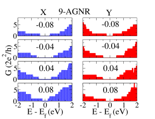
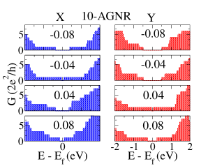
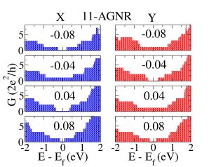
Fig.5 shows the quantum conductance of the 9, 10 and 11-AGNR under various induced and at T = 0 K. Only electrons at play a role in the quantum conductance. The 9 and 10-AGNR, at every induced strain, have zero conductance but for the 11-AGNR there are two special strains ( = -0.04 and = 0.04) wherein the ribbon conductance is nonzero due to a narrow gap. At finite temperature, every subbands near the can contribute to the quantum conductance. Current for a finite bias voltage () is given by Mujica et al. (1994):
| (1) |
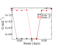
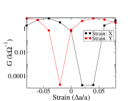
where is the Fermi-Dirac distribution function and is the chemical potential. At a finite temperature has a Gaussian peak that at T = 0 K becomes a Dirac delta function. We estimate that at room temperature the current can be approximated by integrating over . Fig. 6 shows the conductance () of an AGNR family versus strain at room temperature. Because of relatively high band gap of the 9-AGNR, it has a relatively low conductance at room temperature for a wide range of strains (Fig 6(a)). However, the 10 and 11-AGNR have transition between two conductance levels for the compressive and the tensile strains. Fig. 6(b) shows the conductance of a 10-AGNR that was computed from Eq. 1. For and , the AGNR is an insulator while for other strain values it is a conductor. As shown in Fig. 6(c) the conductance of the 11-AGNR for strain values of and decreases due to the increase of the band gap.
We now present the electronic structure of an ZGNR at zero strain. Fig. 7 presents the band structures, the density of states and the quantum conductance of an ZGNR. The band structure near the has a linear dispersion and the group velocity near this level is about . To calculate the conductance and the density of states we construct the wave functions in the energy window with eV around the that is taken to be the reference zero. Quantum transport of the ZGNR near the valence band edge is about .
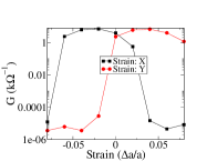
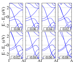
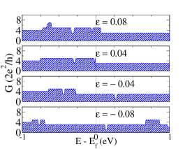
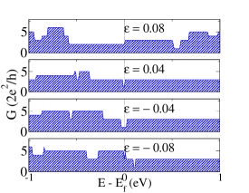
Fig. 8 shows the band structure of a ZGNR under various uniaxial strains. The induced cause an increase in the group velocity of the Dirac fermions from to maximum for the strain from -0.08% to 0.08% (Fig. 8(a)), but the induced cause an decrease in the group velocity from to minimum for the same strain range (Fig. 8(b)). The variation in the band structures influence the electrical conductance of the GNR. Fig. 8(c) and 8(d) show the quantum conductance of the ZGNR under various and . By comparing these results with those related to the relaxed ZGNR (Fig. 7) we find that the strain can increase the conductance of the ZGNR up to two times. The compressive shifts some bands to below the but doesn’t change the quantum conduction near the , while the tensile enhances it to . In the direction, the ZGNR is very sensitive to the strain and the tensile causes an increase in the conductance, while the compressive decreases it at first but increases later.
IV Conclusions
Density functional studies of strain effects on the electrical transport properties of the graphene nanoribbons are presented. By applying a uniaxial tensile strain in the and directions, the electronic properties of the graphene nanoribbons were studied. Using the Wannier functions, the band structure and density of states were calculated for different strains from to . It is observed that as the strain increases, depending on AGNR family type, the electrical conductivity changes from an insulator to a conductor, and this is accompanied by the variation in the electron and hole effective masses. Compressive in the ZGNR shifts some bands to below the and the quantum conductance does not change but the tensile causes an increase in the quantum conductance to near the . In the transverse direction, the ZGNR is very sensitive to the strain and the tensile causes an increase in the conductance while the compressive decreases it at first but increases later.
Acknowledgements.
H. R-T. acknowledges the support from Iran National Science Foundation. We thank Dr. M. Farjam for useful discussions.References
- Neto et al. (2009) A. H. C. Neto, F. Guinea, N. M. R. Peres, K. S. Novoselov, and A. K. Geim, Rev. Mod. Phys. 81, 109 (2009).
- Reina et al. (2009) A. Reina, X. Jia, J. Ho, D. Nezich, H. Son, V. Bulovic, M. Dresselhaus, and J. Kong, Nano. Lett. 9, 30 (2009).
- Kim et al. (2009) K. Kim, Y. Zhao, H. Jang, S. Lee, J. Kim, K. Kim, J. Ahn, P. Kim, J. Choi, and B. Hong, Nature 457, 706 (2009).
- Geim and Novoselov (2007) A. K. Geim and K. S. Novoselov, Nat. Mater. 6, 183 (2007).
- Novoselov et al. (2004) K. S. Novoselov, A. K. Geim, S. V. Morozov, D. Jiang, Y. Zhang, S. V. Dubonos, I. V. Grigorieva, and A. A. Firsov, Science 306, 666 (2004).
- Novoselov et al. (2005) K. S. Novoselov, A. K. Geim, S. V. Morozov, D. Jiang, M. I. Katsnelson, I. V. Grigorieva, and A. Dubonos, S. V .and Firsov, Nature 438, 197 (2005).
- Novoselov et al. (2006) K. S. Novoselov, E. McCann, S. V. Morozov, V. I. Fal Ko, M. I. Katsnelson, U. Zeitler, D. Jiang, F. Schedin, and A. K. Geim, Nat. Phys. 2, 177 (2006).
- Cadelano et al. (2009) E. Cadelano, P. L. Palla, S. Giordano, and L. Colombo, Phys. Rev. Lett. 102, 235502 (2009).
- Pereira et al. (2009) V. M. Pereira, A. H. Castro Neto, and N. M. R. Peres, Phys. Rev. B 80, 045401 (2009).
- Pereira and Castro Neto (2009) V. M. Pereira and A. H. Castro Neto, Phys. Rev. Lett. 103, 046801 (2009).
- Farjam and Rafii-Tabar (2009) M. Farjam and H. Rafii-Tabar, Phys. Rev. B 80, 167401 (2009).
- Bao et al. (2009) W. Bao, F. Miao, Z. Chen, H. Zhang, W. Jang, C. Dames, and C. Lau, Nat. Nanotechnol. 4, 562 (2009).
- Souza et al. (2001) I. Souza, N. Marzari, and D. Vanderbilt, Phys. Rev. B 65, 035109 (2001).
- Saito et al. (1998) R. Saito, G. Dresselhaus, and M. S. Dresselhaus, Physical properties of carbon nanotubes (Imperial College Press, 1998).
- Nardelli et al. (2001) M. B. Nardelli, J. L. Fattebert, and J. Bernholc, Phys. Rev. B 64, 245423 (2001).
- Leenaerts et al. (2008) O. Leenaerts, B. Partoens, and F. M. Peeters, Phys. Rev. B 77, 125416 (2008).
- (17) S. Baroni, S. de Gironcoli, A. Dal Corso, and P. Giannozzi, PWscf (Plane-Wave Self-Consistent Field) codes.
- Giannozzi et al. (2009) P. Giannozzi, S. Baroni, N. Bonini, M. Calandra, R. Car, C. Cavazzoni, D. Ceresoli, G. Chiarotti, M. Cococcioni, I. Dabo, et al., J. Phys. Condens. Mat. 21, 395502 (2009).
- Rappe et al. (1990) A. M. Rappe, K. M. Rabe, E. Kaxiras, and J. D. Joannopoulos, Phys. Rev. B 41, 1227 (1990).
- Monkhorst and Pack (1976) H. J. Monkhorst and J. D. Pack, Phys. Rev. B 13, 5188 (1976).
- Marzari and Vanderbilt (1997) N. Marzari and D. Vanderbilt, Phys. Rev. B 56, 12847 (1997).
- Mostofi et al. (2008) A. Mostofi, J. Yates, Y. Lee, I. Souza, D. Vanderbilt, and N. Marzari, Comput. Phys. Commun. 178, 685 (2008).
- Varchon et al. (2007) F. Varchon, R. Feng, J. Hass, X. Li, B. N. Nguyen, C. Naud, P. Mallet, J. Y. Veuillen, C. Berger, E. H. Conrad, et al., Phys. Rev. Lett. 99, 126805 (2007).
- Finkenstadt et al. (2007) D. Finkenstadt, G. Pennington, and M. J. Mehl, Phys. Rev. B 76, 121405 (2007).
- Son et al. (2006) Y. W. Son, M. L. Cohen, and S. G. Louie, Phys. Rev. Lett. 97, 216803 (2006).
- Wang et al. (2007) Z. F. Wang, Q. Li, H. Zheng, H. Ren, H. Su, Q. W. Shi, and J. Chen, Phys. Rev. B 75, 113406 (2007).
- Mujica et al. (1994) V. Mujica, M. Kemp, and M. Ratner, J. Chem. Phys. 101, 6849 (1994).