Josephson effect in Graphene SNS Junction with a Single Localized Defect
Abstract
Imperfections change essentially the electronic transport properties of graphene. Motivated by a recent experiment reporting on the possible application of graphene as junctions, we study transport properties in graphene-based junctions with single localized defect. We solve the Dirac-Bogoliubov-de-Gennes equation with a single localized defect superconductor-normal(graphene)-superconductor (SNS) junction. We consider the properties of tunneling conductance and Josephson current through an undoped strip of graphene with heavily doped -wave superconducting electrodes in the limit . We find that spectrum of Andreev bound states are modified in the presence of single localized defect in the bulk and the minimum tunneling conductance remains the same. The Josephson junction exhibits sign oscillations.
pacs:
74.45.+c, 74.50.+r, 73.23.Ad, 74.78.NaI Introduction
Recent exciting developments in transport experiments on graphene has stimulated theoretical studies of superconductivity phenomena in this material, which has been recently fabricated Nov-1 ; Zhan-1 . A number of unusual features Klein-1 of superconducting state have been predictedAb-1 ; Wil-1 which are closely related to the Dirac-like spectrum of normal state excitationBen-A ; Lee-1 ; Susu-1 ; Osip-1 . In particular, the unconventional normal electron dispertionHir-1 has been shown to result in a nontrivial modification of Andreev reflection and Andreev bound states in Josephson junctionsGlaz-1 with supercomducting graphene electrodesMai-1 ; Ash-1 .
Other interesting consequences of the existence of Dirac-like quasiparticles can be understood by studying superconductivityShir-1 in grapheneMou-1 ; Khv-1 ; Ale-1 ; Mor-1 ; Fog-1 . It has been suggested that superconductivity can be induced in graphene layer in the presence of a superconducting electrode near it via proximity effect Ben-1 ; Volk-1 ; Tit-1 .
In this work, we study Josephson effect and find bound state in grapheneMahdi-1 for tunneling SNS junction with the presence of a single localized defectMou-2 . In this study, we shall concentrate on SNS junction with normal region thickness , where is the superconducting coherence length, and width which has an applied gate voltage across the normal regionMou-3 ; Sal-1 . In the frame of the limit cosidered by Kulik we investigate tunneling conductance in SNS junctions with presence a single localized defect and find that Andreev levels are modified, the minimum tunneling conductance remains the sameKul-1 ; And-1 ; Le-1 .
II Josephson effect in superconductor/normal(graphene)/superconductor junctions with a single localized defect
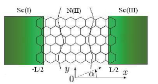
We consider a SNS junction with a single localized defect which is involved in a graphene sheet of width lying in the plane extends from to while the superconducting region occupies (see Fig. 1). The SNS junctions can then be described by the Dirac-Bogoliubov-de-Gennes (DBdG) equationsBen-2 ,
Here , , are the component wave functions for the electron and hole spinors, the index denote or for electrons or holes near and points, takes values for , denotes the Fermi energi, and denote the two inequivalent sites in the hexagonal lattice of graphene, and the Hamiltonian is given by
| (1) |
In Eq. 1, denotes the Fermi velocity of the quasiparticles in graphene and takes values for . The Pauli matrices act on the sublattice index. The excitation energy is measured relative to the Fermi level(set at zero). The electrostatic potential and pair patential have step function profiles, as in the case of a semiconductor two-dimensional electron gas Volk-2 ; Fag-1 ; Gla-1 : , for . We assume non-interacting electrons in the normal region, therefore, , for x L/2. The reduction of the order parameter in the superconducting region on approaching the SN interface is neglected; i.e., we approximate parameter as we have done it above. As discussed by Likharev Lik-1 , this approximation is justified if the weak link has length and width much smaller than . There is no lattice mismatch at the NS interface, so the honeycomb lattice of graphene is unperturbed at the boundary, the interface is smooth and impurity free. Zero magnetic field is assumed.
Solving the DBdG equations, we gain the wave-functions in the superconducting and the normal regions. In region , for the DBdG quasiparticles moving along the direction with a transverse momentum and energy , the wave-functions are given by
The parameters , , , are defined by , , , and denotes region , for and for correspondently. Further we assumed that the Fermi wave length in the superconducting region much smaller than the wave length in the normal region and . Since , this regime of a heavily doped superconductor corresponds to the limits , , .
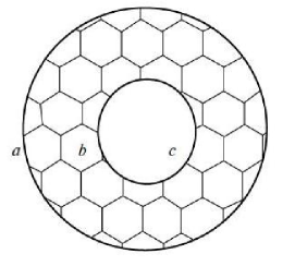
Now we analyze the spectral properties of a graphene ring. Formally we find solutions for graphene ring and then extending ring in the scale, match external boarder of ring with superconducting regions of junction and fix internal part implying which as defect.For that we devide the region into three areas: (see Fig. 2). We solve the DBdG equations for the area , while area is the area where placed defect and area would be extended and matched with superconducting regions. The two valleys decouple, and we can solve equations separately for each valley, , . The term proportional to in Hamiltonian is a mass term confining the Dirac electrons in the area . Rewrite the Hamiltonian in the cylindrical coordinates and since commutes with , its electron-eigenspinors are eigenstates of Ben-ring ,
with eigenvalues , where is a half-odd integer, and is the Bessel function of order. In the plane denotes moving direction of correspondent quasiparticle, for the quasiparticle moving toward and for the quasiparticle moving toward direction correspondently. Further we are interested in to find zero energy statesTit-1 . In this case the DBdG equations posses a general symmetry with respect to the change in the sign of energyYs-1 ,
| (2) |
where we denote and . Thus, for a set of zero modes (,) enumerated by a certain index we should have,
| (3) |
In the same manner as for electron hole-spinors have view,
with the definitions
| (4) | |||
| (5) |
| (6) | |||
| (7) |
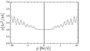
The angle is the angle of incidence of the electron (having longitudinal wave vector ), and is the reflection angle of the hole (having longitudinal wave vector ) Asa-1 ; Bhat-1 . To obtain an analytical approximation of the spectrum, we use the asymptotic form of the Bessel functions for large . This indeed is the desired limit as , where is the defect radius (the radius of the area ) and determine for all eigenvalues . In this limit we impose the infinite mass boundary conditions at , for which in the area with in the and areas consequently (see Fig. 3). Half-odd integer values reflect the Berry’s phase of closed size of a single localized defect in graphene.
To obtain the subgap () Andreev bound states, we now impose the boundary conditions at the graphene. The wave-functions in the superconducting and normal regions can be constructed as
| (8) | |||
| (9) |
where are the amplitudes of right and left moving DBdG quasiparticles in region and and are the amplitudes of right(left) moving electrons and holes, respectively, in the normal regionMai-1 . These wave functions must satisfy the boundary conditions,
| (10) |
Since the wave vector parallel to the interface and different wave vectors in the -direction are not coupled, we may solve the problem for a given and we can consider each transverse mode separately. To leading order in the small parameter we may substitute , . After some algebra we obtain equation
| (11) | |||
Eq. 11 differs from equation obtained for SNS junction without a single defect. Eliminating second term in Eq. 11 we could immediately yield reduction of the equation and it earns a essential form for weak SNS junctionsTit-1 . The solution of Eq. 11 is a single bound state per mode,
where
| (12) | |||
| (13) |
| (14) | |||
| (15) |
We don’t have a simple analytic expression for the -dependance but we obtained modified Andreev levels with the presence a single localized defect in the bulk. The conductance of the graphene strip is expressed through the transmission probability by the Landauer formula,
| (16) |
where is given by =Int. Substitution transmission probability into Eq. 16 gives the conductance (normalized per mode) versus Fermi energy (see in Fig. 3).
III Josephson current
The Josephson current at zero temperature is given by
| (17) |
where the factor of 4 accounts for the twofold spin and valley degeneracies. Substitution of into Eq. 17 gives the supercurrent due to the discrete spectrum
| (18) |
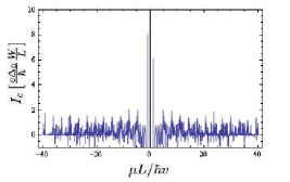
Contributions to the supercurrent from the continuous spectrum are smaller by a factor and may be neglected in the short-junction regimeBen-A . For the summation over may be replaced by an integration. The resulting Josephson current upon substitution is plotted as a function of in Fig. 4.
IV CONCLUSION
In conclusion, we have shown that a Josephson junction in graphene can carry a nonzero supercurrent even if the Fermi level is tuned to the point of zero carrier concentration. At this Dirac point, the current-phase relationship has a resonant behaviour due to single localized defect. This unusual ”quasidiffusive” behaviour of the Josephson effect in undoped graphene should be observable in submicrometer scale junctions. It is found that the current has a peak-like structure, with alternating signs of the peaks. The resulting nonequilibrium Josephson current for a given phase difference thus oscillates as a function of chemical potential, i.e the junction displays so-called -behaviour.
V ACKNOWLEDGMENT
Authors thank Prof. H.H. Lin for fruitful discussions and an anonymous referee for interesting comments and suggestions which allowed us to improve this work. We acknowledge support from the National Center for Theoretical Sciences in Taiwan.
References
- (1) K.S. Novoselov, A.K. Geim, S.V. Morozov, D. Jiang, M.I. Katsnelson, I.V. Grigorieva, S.V. Dubonos, and A.A. Firsov, Nature 438, 197 (2005).
- (2) Y. Zhang, Y.-W. Tan, H.L. Stormer, and P.Kim, Nature 438, 201 (2005).
- (3) P. Kleinert, Physica B: Cond. Matt. 404, 4015-4017 (2009); Dima Bolmatov, Chung-Yu-Mou, Physica B: Condensed Matter 405, 2896-2899 (2010); P. Kleinert, epriint: arXiv:0802.1271v1.
- (4) D. A. Abanin, S. A. Parameswaran, and S. L. Sondhi, Phys. Rev. Lett. 103, 076802 (2009); B. zyilmaz1, P. Jarillo-Herrero1, D. Efetov, D. A. Abanin, L. S. Levitov, and P. Kim, Phys. Rev. Lett. 99, 166804 (2007); D. A. Abanin, P. A. Lee, and L. S. Levitov, Phys. Rev. Lett. 96, 176803 (2006).
- (5) P. Ghaemi, F. Wilczek, arXiv:070 9.2626v1.
- (6) C. W. J. Beenakker and H. van Houten, Phys. Rev. Lett. 66, 3056 (1991).
- (7) Q.-H. Wang and D.-H. Lee, Phys. Rev. B 67, 20511 (2003).
- (8) S. Saito and Alex Zettl, CARBON NANOTUBES: QUANTUM CYLINDERS OF GRAPHENE,( Elsevier, Oxford, 2008).
- (9) D. V. Kolesnikov and V. A. Osipov, JETP Lett. 87, 419 422 (2008).
- (10) H. Kawai, Y. Yoshimoto, O. Narikiyo, Y. Hanawa, A. Imamura, Surface Science 602, 3010-3017 (2008).
- (11) J. Koch, V. Manucharyan, M. H. Devoret, and L. I. Glazman, Phys. Rev. Lett. 103, 217004 (2009).
- (12) M. Maiti and K. Sengupta, Phys. Rev. B 76, 054513 (2007).
- (13) P. Ghaemi, Fa Wang, and Ashvin Vishwanath, Phys. Rev. Lett. 102, 157002 (2009).
- (14) P. M. Shirage, K. Kihou, K. Miyazawa, C.-H. Lee, H. Kito1, H. Eisaki, T. Yanagisawa, Y. Tanaka, and A. Iyo, Phys. Rev. Lett. 103, 257003 (2009).
- (15) H.H. Lin, T. Hikihara, H.T. Jeng, B.L. Huang, and C.Y. Mou, X. Hu, Phys. Rev. B 79, 035405 (2009).
- (16) D.V. Khveshchenko, J. Phys.: Condens. Matter 21, 075303 (2009).
- (17) I.L. Aleiner, D.E. Kharzeev, and A.M. Tsvelik, Phys. Rev. B 76, 195415 (2007).
- (18) A.F. Morpurgo, F. Guinea, Phys. Rev. Lett. 97, 196804 (2006).
- (19) M.M. Fogler, D.S. Novikov, and B.I. Shklovskii, Phys. Rev B 76, 233402 (2007).
- (20) C.V.J. Beenakker , Phys. Rev. Lett., 97, 067007 (2006).
- (21) A.F. Volkov, P.H.C. Magnee, B.J. van Wees, and T.M. Klapwijk, Physica C 242, 261 (1995).
- (22) M. Titov and C.W.J. Beenakker, Phys. Rev. B 74, 041401(R) (2006).
- (23) M. Zarea, N. Sandler, Physica B: Cond. Matt. 404, 2694-2698 (2009).
- (24) B.L. Huang and C.Y. Mou, EPL 88, 68005 (2009); D. Bolmatov, Chung-Yu Mou, JETP 110, 612-616 (2010).
- (25) S.T. Wu and C.Y. Mou, Phys. Rev. B 67, 024503 (2003).
- (26) E. Zhao and J.A. Sauls, Phys. Rev. Lett. 98, 206601 (2007).
- (27) I.O. Kulik and A. Omelyanchuk, JETP Lett. 21, 96 (1975); Sov.Phys. JETP 41, 1071 (1975).
- (28) A.F. Andreev, Zh. Eksp. Teor. Fiz. 46, 1823 (1964).
- (29) P.A. Lee, Phys. Rev. Lett. 71, 1887 (1993).
- (30) C.W.J. Beenakker, cond-mat/0604594.
- (31) A.F. Volkov, P.H.C. Magnee, B.J. van Wees, and T.M. Klapwijk, Physica C 242, 261 (2006).
- (32) G. Fagas, G. Tkachov, A.Pfund, and K. Richter, Phys. Rev. B 71, 224510 (2005).
- (33) M.G. Vavilov, I.L. Aleiner, and L.I. Glazman, Phys. Rev. B 76, 115331 (2007).
- (34) A review of superconducting weak links is K. K. Likharev, Rev. Mod. Phys. 51, 101 (1979).
- (35) P. Recher, B. Trauzettel, A. Rycerz, Ya.M. Blanter, C.W.J. Beenakker, and A.F. Morpurgo, Phys. Rev. B 76, 235404 (2007).
- (36) A.P. Isaev and O.V. Ogievetsky, J. Phys. A: Math. Theor. 42, 304017 (2009); S. I. Bastrukov, P.-Y. Lai, I. V. Molodtsova, H.-K. Chang, D. V. Podgainy, SRL 16, 5-10 (2009).
- (37) Y. Asano, T. Yoshida, Y. Tanaka, and Alexander A. Golubov, Phys. Rev. B 78, 014514 (2008).
- (38) S. Bhattacharjee and K. Sengupta, Phys. Rev. Lett. 97, 217001 (2006).