Current-voltage (I-V) characteristics of armchair graphene nanoribbons under uniaxial strain
Abstract
The current-voltage (I-V) characteristics of armchair graphene nanoribbons under a local uniaxial tension are investigated by using first principles quantum transport calculations. It is shown that for a given value of bias-voltage, the resulting current depends strongly on the applied tension. The observed trends are explained by means of changes in the band gaps of the nanoribbons due to the applied uniaxial tension. In the course of plastic deformation, the irreversible structural changes and derivation of carbon monatomic chains from graphene pieces can be monitored by two-probe transport measurements.
pacs:
72.80.Vp, 62.25.-g, 77.80.bnI Introduction
Graphene, as a (2D) monolayer honeycomb structure of carbon, has attracted a great deal of interest since its successful preparation in 2004.gra2004 Due to its unique mechanical, structural and electronic properties, graphene have been realised as an important material for numerous theoretical investigations and promising applications. Among these are charge carriers behaving as massless Dirac fermions,dirac Klein tunneling,klein1 ; klein2 ballistic transport at room temperature,ballistic1 ; ballistic2 and anomalous quantum Hall effects.qhe From experimental points of view, field-effect transistorstransistor1 ; transistor2 , micromechanical resonatorsresonator , gas sensorsgas_sensor of graphene have already been proposed. Most of these are directly related with its transport properties.
Earlier transport studies predict that spin-valve devices based on graphene nanoribbons can exhibit magnetoresistance values that are thousands of times higher than previously reported experimental values.magnetorezistance Unusual effects of dopings on the transport properties of graphene nanoribbons were also reported.doping1 ; doping2 ; hasan Nevertheless, the transport properties of graphene nanoribbons under uniaxial tension have not been fully explored even from the theoretical points of view. While the effect of strain on the electronic properties of graphene is becoming an active field of study,neto the transport properties and I-V characteristics of nanoribbons under local or uniform strain is of crucial interest for development of future device applications.
In this study, based on state-of-the-art first-principles quantum transport calculations, we investigate the effects of uniaxial strain on the current-voltage (I-V) characteristics of graphene nanoribbons. We showed that elastic strain can alter the electron transport properties dramatically. In some cases, under a 10% strain, the current can change as much as 400-500 %. However, the variation of current with strain is sample specific. Even more remarkable is that the chain formation of carbon atoms from the graphene nanoribbonsiijima ; mehmet_kopma undergoing a plastic deformation can be monitored through I-V characteristics showing negative differential resistance.
II MODEL AND METHODOLOGY
Geometry relaxations and electronic structures are calculated by using SIESTA package,siesta which uses numerical atomic orbitals as basis sets and Troullier-Martin typeTM norm-conserving pseudopotentials. The exchange-correlation functional of the generalized gradient approximation is represented by the Perdew-Burke-Ernzerhof approximation.pbe A 300 Ryd mesh cut-off is chosen and the self-consistent calculations are performed with a mixing rate of 0.1. The convergence criterion for the density matrix is taken as 10-4. Brillouin zone (BZ) sampling of the calculations have been determined after extensive convergence analysis. The conjugate gradient method is used to relax all the atoms until the maximum absolute force was less than 0.05 (eV/Å). Interactions between adjacent graphene layers is hindered by a large spacing of 10 Å.
The electronic transport properties are studied by the non-equilibrium Green’s function (NEGF) techniques, within the Keldysh formalism, based on density functional theory (DFT) as implemented in the TranSIESTA (Ref. transiesta, ) module within the SIESTA (Ref. siesta, ) package. A single -plus-polarization basis set is used. Test calculations with larger basis set and mesh cut-off were also performed, which give almost identical results. The current through the contact region was calculated using Landauer-Buttiker formula,buttiker
| (1) |
where G) is the unit of quantum conductance and is the transmission probability of electrons incident at an energy E through the device under the potential bias . The electrochemical potential difference between the left and right electrodes is .
III I-V characteristics under elastic strain
The band gaps of armchair graphene nanoribbons (AGNRs), which we consider in this study, depend on their widths,cohen_prl which are conventionally specified according to the number of dimer lines, in their primitive unit cell. AGNR()’s are grouped into three families, namely family having smallest band gaps, the family having medium band gaps, and family having largest gaps, where is an integer. Band gaps of each family decrease with increasing and eventually goes to zero as . AGNRs are nonmagnetic direct band gap semiconductors, which can, however, be modified by vacanciesmehmet_delik and impurities.haldun_tm
The NEGF technique used to study the electronic transport employs a two-probe system; semi-infinite left- and right-electrode regions are in contact with a confined central scattering region. A two-probe system, specific to AGNR with , but representative of any , is shown in Fig. 1 (a). Both electrodes and the central region are made from AGNR(). Periodic boundary conditions were imposed on the plane perpendicular to the axis of the nanoribbon. The carbon atoms at the edges are saturated with H atoms. The central region contains primitive unit cells, with a total length of 21.76 Å (). The length of the central region is sufficient enough to avoid an abrupt change in electronic structure while progressing from the electrode region to the strained region of interest.
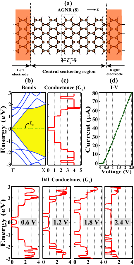
We first consider the electronic transport properties of the unstrained two-probe system presented in Fig. 1 (a). To provide for an intuitive understanding of the transport phenomena, the band structure of the electrodes or the scattering region in their primitive unit cell are shown in Fig. 1 (b). The lowest conduction and highest valance bands originate from - and -states, respectively. Unlike the perfect 2D graphene, where - and -bands cross at the -corners of BZ, AGNR(8) is a direct band gap material having 0.20 eV band gap value. The calculated zero-bias transmission spectrum is given in Fig. 1 (c), which apparently mimics the band structure of AGNR(8). There is a region of zero-transmission with a width of eV and located around the Fermi level, coinciding with the band gap of AGNR(8). Likewise, the step-like behavior of the spectrum is related with the available conductance channels due to bands. The current as a function of the applied bias voltage is presented in Fig. 1 (d). For this type of calculations, we increased in steps of 0.1 V and used the converged density matrix of the previous state as an initial guess for the next step. Applying a bias voltage shifts the Fermi level of the left-electrode with respect to the Fermi level of the right-electrode. The current starts flowing once the top of the valence band of the left-electrode matches in energy with the bottom of the conduction band of the right-electrode, as expected from the T(E, ) for low-bias values. The T(E,) does not alter much with the bias, since it is a uniform system and no significant permanent charge migrations should occur. This is evident from the linear response of the current to the bias voltage for values of eV. As the calculation of the current is very time consuming, the bias range is limited from 0 to 2.5 V. In Fig. 1 (e) the transmission spectrums for bias voltages of 0.6 V, 1.2 V, 1.8 V and 2.4 V are also presented. As readily seen, the transmission T(E,) contributing to the current always keep near 1 G0, and the higher values in transmission values move further away from the Fermi energy. This is due to the fact that as the bands of the leads move up or down in energy scale with the varying bias, only a single conduction channel is open, or in other words, only one band crosses the energy of interest, at either one or both of the leads. This holds true for the bias voltages we consider in this study and as a result, we see a linear current response to voltage for zero-strain.

Earlier, we have investigated the elastic and plastic deformation of graphene and its nanoribbons under uniaxial tension.mehmet_kopma Mechanical properties were revealed from the strain energy, ; namely, the total energy at a given uniaxial strain minus the total energy at zero-strain. Here, the uniaxial strain is , where and are equilibrium and stretched lattice constants of the nanoribbon, respectively. The tension force, and the force constant are obtained from the strain energy. Calculated elastic constants were in good agreement with available experimental data obtained from graphene.gr_exp Here we consider the I-V characteristics of AGNR(8) under a uniform uniaxial tension of the central scattering region for . The strain is introduced as follows: The electrode atoms are fixed in their equilibrium positions while the length of the central region is increased uniformly by . Subsequently, the structure of the central region is fully optimized in a larger supercell containing also unstrained electrode regions. In this respect, our study reveals the effect of a local strain in a long unstrained nanoribbon. The total energy of the system is recalculated. The strain energy , is obtained according to above definition. versus the elongation , as well as plot for AGNR(8) system is given in Fig. 2 (a). The segment of AGNR(8) in the central scattering region undergoes an elastic deformation up to strain values , where the honeycomb-like structure is maintained, and the system returns to its original configuration if the tension is released. However, for higher values of strain, the system deforms plastically, where irreversible structural changes occur and the strain energy suddenly drops. Further information for this type of elastic and plastic deformation can be found in Ref.mehmet_kopma, .
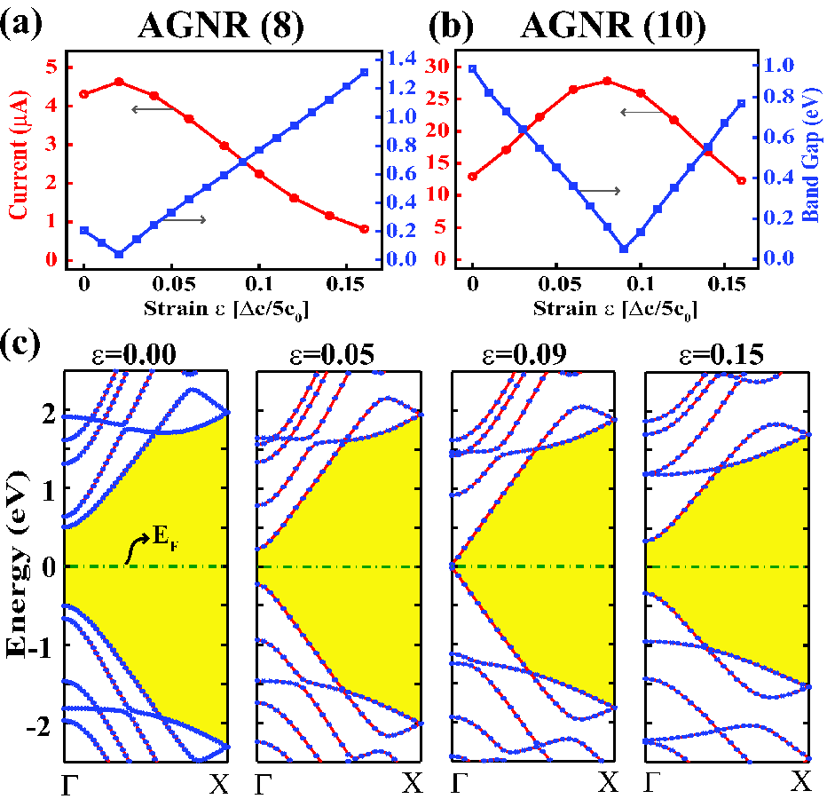
In Fig. 2 (b)-(d), we present the I-V plots of stretched nanoribbons. The electrode regions are identical to the no-strain case, but the central region under strain causes the changes. Once again, due to the band gap of the electrodes of 0.2 eV in AGNR(8), no current is observed up to a bias voltage of 0.2 V. The current response to bias voltage is linear for low strain, but becomes increasingly non-linear for higher strain. It is important to notice that higher strain in the central region induces stronger non-uniformity on its geometry and thus on its electronic structure as compared to the electrodes. Equilibrium charge transfer may occur and alter the systems response to the non-equilibrium perturbation. This will result in a varying T(E,) for different values of . It is informative to compare the current values for systems under different strain at a given bias voltage. For example, at =2 V, the current is around 62 at . It increases to 65 at , but steadily decreases for higher strain, having values of 28 at and 12 at . One also notes that the I-V curve in Fig. 1 (d), which is almost linear for , starts to lose its linearity for higher values of strain as seen from Fig. 2 (b).
Other ribbons such as AGNR(6) and AGNR(10) whose I-V characteristics are given in Fig. 2 (c) and (d). AGNR(6) belongs to the family and it has a larger band gap (1.04 eV) as compared to AGNR(8). As a result, we do not observe a current until 1 eV as seen from Fig. 2 (c). The current steadily decreases until , then starts to increase as seen from Fig. 2 (c). AGNR(10) is another system which has a band gap value around 1.00 eV and its I-V characteristics are given in Fig. 2 (d). In contrast to AGNR(6), the current first increases until and then starts to decrease for higher strain values. All these results in Fig. 2 (b),(c), and (d) show that the current passing through nanoribbons is very sensitive to the strain values and the behaviors of I-V curves are sample specific.
The increase and decrease of the currents given in Fig. 2 due to the changes in the strain is directly related with the electronic structure of the central scattering region, which is modified as a result of changes in atomic structure under tension.mehmet_kopma ; hakem In Fig. 3 (a) we show the variation of current and band gap of AGNR(8) with applied uniaxial strain. Here current values are extracted from Fig. 2 (b) for 2 V bias voltage. As seen from the plots, there is an inverse relationship between the current and band gap values. Any increase in the band gap decreases the current and vice versa. The same analysis performed for AGNR(10) in Fig. 3 (b) also confirms this relationship. The changes in the band structures of AGNR(10) can also be followed from Fig. 3 (c), where the lowest conduction and highest valence bands approach to each other until and then move away for higher values of strain. The band gap variations occur due to different nature of bands around the conduction and valence band edges exhibiting different shifts with strain. In particular, note that - and -bands of AGNR(10) cross linearly at -point by closing the band gap. This is the realization of massless Dirac Fermion behavior in a nanoribbon, which is semiconductor under zero-strain.mehmet_kopma In a simple model, an electron is ejected from the left electrode at an energy value lower than the shifted valence band maximum, for available ranges within the bias voltage. It is incident upon the central region, with lower chemical potential, and tunnels through to the right electrode, still lower in energy. The smaller the band gap value for the central region, the larger the number of possible states that participate in the tunneling, thus the larger is the value of the current.
IV Transport properties of AGNR(8) under plastic deformation
While the elastic deformation imposes changes in the band gap and current values, the onset of plastic deformation results in dramatic changes in the structure. After yielding, the modification of honeycomb structure is somehow stochastic and sample specific. It depends on the conditions, such as the defects in the sample, the temperature effects and the rate of stretching. However, it has been shown theoreticallymehmet_kopma that under certain circumstances a long carbon atomic chaintongay (identified as cumulene having double bonds and polyyne with alternating triple and single bonds) can form in the course of plastic deformation of graphene, unless the edges of AGNR is not terminated with hydrogen. Upon further stretching, each carbon atom of graphene implemented to chain results in a stepwise elongation of the chain between two graphene pieces. Monatomic carbon chain, which was derived experimentally from graphene,iijima can be a potential nanostructure for various future applications. The important issue we address here is how these sequential structural changes reflects the transport properties.
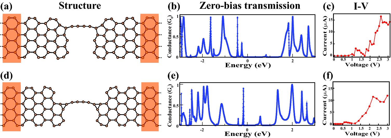
In Fig. 4 (a) we present the atomic structure of a two-probe graphene nanoribbon system which is formed after the plastic deformation of AGNR(8) nanoribbon. A short chain containing 4 carbon atoms between the graphene flakes is formed in the scattering region and its zero-bias transmission spectrum is presented in Fig. 4 (b). This spectrum is composed of peaks rather than step-like levels as in Fig. 1 (c). The calculated I-V plot in Fig. 4 (c) also contains some peaks, which may lead to negative differential resistance.cohen_differential Similar situation also exists for a longer chain in Fig. 4 (d), which occurred at a more advanced stage of plastic deformation whereby the nanoribbon in the central region is more stretched than in Fig. 4 (a). At the end, two more carbon atoms are included to the chain. The differences between zero-bias transmission curves in Fig. 4(b) and (e) occur because of the energy level diagram and their positions relative to Fermi levels are different. Also, the I-V curve corresponding to two carbon chains of different lengths occurring in subsequent stages of stretching are rather different. We note that the conductance of the longer carbon chain in Fig. 4(d) and the corresponding current values (I) of a given bias voltage (V) can be higher than the shorter chain in Fig. 4(a). This paradoxical situation is related with the fact that some energies of the channels can be closer to the Fermi level as the length of the chain increases.lang Further stretching of the system shown in Fig. 4(d) can produce longer carbon chain structures. The length of these chains can be as long as 10 carbon chains. As found for the structures in Fig. 4(a) and Fig. 4(d), the I-V characteristics of the longer carbon chains will be different and will allow one to monitor the structural changes. Finally the plastic deformation terminates upon breaking of the chain.
V Conclusion
We have shown that the transport properties of the segment of an armchair graphene nanoribbon in a two-probe system can be modified with uniaxial strain. The current under a fixed bias can change several times with applied uniaxial strain. However, these changes are sample specific and related with strain induced changes in the electronic structure near the band gap. Irreversible structural changes and the formation of monatomic carbon chain between graphene pieces in the advanced stages of plastic deformation can be monitored through two-probe transport experiments. We believe that our findings are of crucial importance for recent active studies aiming to reveal the effects of strain on the electronic properties of graphene. Also our results suggest that these systems can be used as nanoscale strain gauge devices.
VI Acknowledgement
Part of the computations have been provided by UYBHM at Istanbul Technical University through a Grant No. 2-024-2007. S.C. acknowledges financial support from The Academy of Science of Turkey (TUBA).
References
- (1) K. S. Novoselov, A. K. Geim, S. V. Morozov, D. Jiang, Y. Zhang, S. V. Dubonos, I. V. Grigorieva, A. A. Firsov, Science 306, 666 (2004).
- (2) K.S. Novoselov, A.K. Geim, S.V. Morozov, D.Jiang, M.I. Katsnelson, I.V. Grigorieva, S.V. Dubonos, and A.A. Firsov, Nature (London) 438, 197 (2005).
- (3) M. I. Katsnelson, K. S. Novoselov, and A. K. Geim, Nature Phys. 2, 620 (2006).
- (4) A. F. Young and P. Kim, Nature Physics 5, 222 (2009).
- (5) D. Gunlycke, H. M. Lawler, and C. T. White, Phys. Rev. B 75, 085418 (2007).
- (6) X. Du, I. Skachko, A. Barker and E. Y. Andrei, Nature Nanotechnology 3, 491 (2008).
- (7) K. S. Novoselov, Z. Jiang, Y. Zhang, S. V. Morozov, H. L. Stormer, U. Zeitler, J. C. Maan, G. S. Boebinger, P. Kim, and A. K. Geim, Science 315 (5817), 1379.
- (8) X. Wang, Y. Ouyang, X. Li, H. Wang, J. Guo, and H. Dai, Phys. Rev. Lett. 100, 206803 (2008).
- (9) Y.-M. Lin, C. Dimitrakopoulos, K. A. Jenkins, D. B. Farmer, H.-Y. Chiu, A. Grill, and Ph. Avouris, Science 327 (5966), 662.
- (10) J. Scott Bunch, Arend M. van der Zande, Scott S. Verbridge, Ian W. Frank, David M. Tanenbaum, Jeevak M. Parpia, Harold G. Craighead, and Paul L. McEuen, Science 315 (5811), 490.
- (11) F. Schedin, A. K. Geim, S. V. Morozov, E. W. Hill, P. Blake, M. I. Katsnelson, and K. S. Novoselov, Nature Materials 6, 652 (2007).
- (12) W. Y. Kim, and K. S. Kim, Nature Nanotechnology 3, 408 (2008).
- (13) B. Biel, X. Blase, F. Triozon, and S.Roche, Phys. Rev. Lett. 102, 096803 (2009).
- (14) Qimin Yan, Bing Huang, Jie Yu, Fawei Zheng, Ji Zang, Jian Wu, Bing-Lin Gu, Feng Liu, and, Wenhui Dua, Nano Letters 2007 7 (6), 1469-1473
- (15) H. Şahin and R. T. Senger, Phys. Rev. B 78, 205423 (2008).
- (16) V. M. Pereira and A. H. Castro Neto, Phys. Rev. Lett. 103, 046801 (2009).
- (17) C. Jin, H. Lan, L. Peng, K. Suenaga, and S. Iijima, Phys. Rev. Lett 102, 205501 (2009).
- (18) M. Topsakal and S. Ciraci, Phys. Rev. B 81, 024107 (2010).
- (19) J. M. Soler, E. Artacho, J. D. Gale, A. Garcia, J. Junquera, P. Ordejon, and D. Sanchez-Portal, J. Phys.: Condens. Matt. 14, 2745 (2002).
- (20) N. Troullier and J. L. Martins, Solid State Commun. 74, 613 (1990).
- (21) J. P. Perdew, K. Burke and M. Ernzerhof, Phys. Rev. Lett. 77, 3865 (1996).
- (22) We used the software-package SIESTA-3.0-b as distributed by the SIESTA group (͑www.uam.es/siesta), which implements the method described in: M. Brandbyge, J.-L. Mozos, P. Ordejon, J. Taylor, and K. Stokbro, Phys. Rev. B 65, 165401 (2002).
- (23) S. Datta, in Electronic Transport in Mesoscopic Systems, edited by H. Ahmed, M. Pepper, and A. Broers Cambridge University Press, Cambridge, England, 1995.
- (24) Y.W Son, M. L. Cohen and S. G. Louie, Phys. Rev. Lett. 97, 216803 (2006).
- (25) M. Topsakal, E. Akturk, H. Sevinçli, S. Ciraci, Phys. Rev. B 78, 235435 (2008).
- (26) H. Sevincli, M. Topsakal, E. Durgun and S. Ciraci, Phys. Rev. B, 77, 195434 (2008).
- (27) C. Lee, X. Wei, J.W. Kysar, J. Hone, Science 321, 385 (2008).
- (28) Y. Lu, and J. Guo, Nano Res, 3, 189 (2010).
- (29) S. Tongay, R.T. Senger, S. Dag and S. Ciraci, Phys. Rev. Lett. 93, 136404 (2004)
- (30) K. H. Khoo, J. B. Neaton, Y. W. Son, M. L. Cohen, and S. G. Louie, Nano Letters 8, 2900 (2008).
- (31) N. D. Lang and Ph. Avouris, Phys. Rev. Lett. 81, 3515 (1998).