Charged defects in graphene and the ionicity of hexagonal boron nitride in direct images
Abstract
We report on the detection and charge distribution analysis for nitrogen substitutional dopants in single layer graphene membranes by aberration-corrected high-resolution transmission electron microscopy (HRTEM). Further, we show that the ionicity of single-layer hexagonal boron nitride can be confirmed from direct images. For the first time, we demonstrate by a combination of HRTEM experiments and first-principles electronic structure calculations that adjustments to the atomic potentials due to chemical bonding can be discerned in HRTEM images. Our experiments open a way to investigate electronic configurations in point defects or other non-periodic arrangements or nanoscale objects that can not be studied by an electron or x-ray diffraction experiment.
I Introduction
The elastic scattering of high-energy electrons within a material, as detected by electron diffraction, electron holography or high resolution transmission electron microscopy (HRTEM), probes the distribution of the internal electrostatic potential KirklandEMcomputing ; Buseck_HRTEMandAssoc of a sample. This potential is given by the Coulomb potential of the nuclei, screened by the electrons. The dominant contribution to the electrostatic potential comes from the core region, i.e. the region close to the nucleus. However, only the valence electrons participate in chemical bonds and are rearranged depending on the atomic configuration. Therefore, HRTEM images are usually dominated by structural information, i.e. the position of the atoms rather than the electronic configuration. The effect of bonding on HRTEM image contrast has been explored in previous studies AbInitioHRTEMGeming98 ; AbInitioInterfaceTEMMogck04 ; DengMarksBonding06 ; DengGlowingDefects07 ; however, it was concluded that the predicted effects would be difficult to detect experimentally. This has led to the assumption that conventional (independent atom model, IAM) HRTEM image simulation is sufficient for structural and elemental identification. The effect of binding electrons has been detected experimentally in electron diffraction experiments SpenceBondMap99 ; CBEMoribe02 , but so far was not discerned in TEM images. However, diffraction experiments are limited to periodic structures and sufficiently large samples. Here, we study these chemical shifts for a point defect, the nitrogen dopant NdopedGr09 in graphene Novoselov2004Sci ; GeimGrapheneReview07 , and few-nm sized hexagonal boron nitride mono-layer membranes MeyerBNnl09 ; IijimaBN09 ; ZettlHbn2009 ; KrivanekBNnature10 . The precisely defined sample geometries in terms of thickness (one layer), amorphous adsorbates and defects (none in the selected regions), along with very high sample stability and therefore unprecedented signal to noise ratios (by using lower acceleration voltages to avoid sample damage) enable sufficiently accurate measurements DengMarksBonding06 . Both, HRTEM experiments and first-principles electronic structure calculations, show that the IAM is not sufficient for accurate TEM image simulations of these materials. Our experiments open a new way to study electronic configurations, in particular for point defects, other non-periodic arrangements, or nanoscale objects that can not be analyzed in a diffraction experiment.
II Methods summary
We prepared nitrogen doped graphene membranes by following the CVD methods for graphene synthesis CVDKimNature09 ; CVDCopperRuoff09 ; CVDNiHyeJin10 , with the addition of small amounts of ammonia as nitrogen source NdopedGr09 during the growth. We have used both the CVD growth on nickel substrates and on copper substrates, and in both cases the addition of ammonia into the reaction has led to nitrogen doped graphene sheets. We transfer the CVD grown graphene sheets to commercial TEM grids as described previously CVDNiHyeJin10 . Single-layer hexagonal boron nitride is prepared and imaged as described previously MeyerBNnl09 . TEM imaging is carried out using an image-side aberration corrected Titan 80-300, operated at 80kV. The spherical aberration is set to ca. 20m and a defocus of (Scherzer defocus) and (Graphene lattice in the second extremum of the contrast transfer function (CTF)) is used. Drift-compensated averages of 20-40 CCD exposures are used. Post-filtering of the images is needed to discover the N substitution defects in our experimental data. Shown here is the example of a Fourier filter that removes the periodic components of the graphene lattice, and a simple gaussian low-pass filter chosen so that the graphene lattice contrast is reduced to ca. 0.5% (in this case the N substitution and graphene lattice appear with similar contrast). TEM image simulations for the bonded atomic configuration follows the procedure pioneered by Deng and Marks DengMarksBonding06 with some modifications. In brief, a relaxed atomic configuration is obtained using the VASP DFT code Kresse96 which is well-suited to perform large scale geometry optimizations in graphene-like systems from first principles Kuenzel2009 . Then, the WIEN2k DFT code WIEN2k2001 is used to obtain the all-electron self-consistent electron density and corresponding electrostatic potentials for this configuration. The TEM image simulation is then based on projections of this electrostatic potential, and follows the approximations for thin specimen as in Chapter 3 of Ref. KirklandEMcomputing . Further details of the sample preparation and characterization, DFT calculations, potential calculations, TEM image simulation, further TEM images, and a detailed analysis of residual aberrations are described in the supplementary information.
III Nitrogen doped graphene
Nitrogen doped graphene in our case refers to a substitutional doping, i.e. a small fraction of carbon atoms (ca. 0.1%) was replaced by nitrogen during synthesis. This configuration has been considered in many previous works (e.g. NsubstDistAndCH05 ; NsubstCNTbondlength07 ), and it was found that the C-N bond length in this configuration is nearly identical to the C-C bond length in graphene (with differences less than 2pm). Our own DFT-relaxed configuration (Fig. 1a) is in agreement with these earlier works, and is used for all TEM simulations of this defect.
Fig. 1 shows calculated TEM images with and without the inclusion of bonding effects. Images labeled as “IAM” (Fig. 1b-i) are based on the so-called independent atom model. In this model, the potential and charge distribution of the specimen is calculated as a superposition of potentials and charge densities that have once been calculated for an isolated atom of each element. This is the conventional model for TEM image simulation. We show here two different imaging conditions (defocus and ), and two filters (which are needed to discover the defect in experimental data), as described in the methods. Remarkably, the nitrogen substitution defect is expected to be practically invisible (less than 0.1% contrast) within the IAM, i.e., when bonding effects are not taken into account. On the contrary, charge densities and potentials obtained from the DFT calculation naturally contain the electronic configuration of the bonded situation (corresponding images are labeled with “DFT”). TEM image simulations based on the accurate electrostatic potential from the DFT calculation are shown in Fig. 1k-r. Here, we expect a detectable signal when using the DFT based potentials for TEM image simulation: The N substitution is now visible as a weak dark spot, best seen in the filtered images. In the comparison, there is even a change of sign, i.e, a (very weak) white spot in the Fourier filtered images of the IAM (Fig. 1d,h) while there is a stronger (and detectable) dark spot according to the DFT model (Fig. 1m,q).
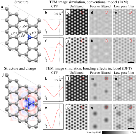
There is a remarkable focus dependence in the DFT based image contrast, shown here by the two different defocus values and . Defocus value represents a standard condition where spherical aberration and defocus are tuned to obtain a single pass-band in the contrast transfer function (CTF, Fig. 1b) that ends approximately at the information limit LentzenReview06 . In this case, shown in Fig. 1b-e, the nitrogen substitution is expected to produce a weak dark spot (0.3% contrast); which is still difficult to detect since it is both a weak and narrow signal. Using a larger defocus (), however, both width and amplitude of the signal increases (Fig. 1f-i). This focus behaviour is contrary to what would be expected for a point scatterer, such as an ad-atom or a charge that is localized on one atom. For this reason, detection of the nitrogen substitution defect in graphene is easier (requiring significantly lower electron doses per area) when using the larger defocus settings.
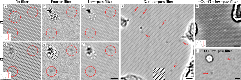
Experimentally, we identify single-layer graphene areas in the nitrogen doped, CVD grown graphene sheets by an electron diffraction analysis as described previously MeyerGrapheneNature07 ; MeyerGrapheneSSC07 . We record long image sequences, >30 exposures with a pixel size of and ca. counts per pixel, for each value of defocus. Importantly, the graphene structure and defects of interest remain stable throughout the long exposure and associated high dose. Then, a drift compensated average of 39 (Fig. 2a-c) or 34 (Fig. 2d-f) exposures provides the very high signal to noise ratio images that are further analyzed. As predicted by the DFT model, they exhibit a weak dark contrast in the larger defocus images (Fig. 2d-f), but disappear in the noise as the focus is set to the optimum (Scherzer defocus) conditions (Fig. 2a-c). Fig. 2a-f are from a nitrogen doped sample synthesized on a nickel surface. Fig. 2g shows an example from N doped graphene grown on copper. Fig. 2h shows two nitrogen substitutions imaged with reversed contrast transfer (negative Cs, positive defocus), where the substitution atoms are revealed as weak white spots. Finally, Fig. 2i shows an alternative way to fabricate atomic substitutions in graphene: Here, an un-doped graphene sample was briefly exposed to higher energy electrons (300kV, ca. ), and subsequently imaged at 80kV to prevent further damage. After such a treatment, we also find nitrogen substitution defects. A likely mechanism is a substitution of beam-generated vacancies by atoms from the residual gas. However, we note that also a variety of other defects is generated by this approach.
The focus dependence of the nitrogen defect in graphene deserves further discussion. As noted above, a contrast that becomes both wider and stronger with larger defocus is contrary to expectations for a point scatterer, such as an ad-atom or a localized charge. It means that the experimentally accessible information, after removing the periodic component of the graphene lattice, contains predominantly lower spatial frequency information. This information is cut off by the CTF (Fig. 1b,k) in the optimum-focus () image of the aberration-corrected microscope. At the larger defocus, the CTF (Fig. 1f, o) shows oscillations but includes more of the lower spatial frequencies, thus revealing the charge associated with the nitrogen defect. It is important to note that we can draw this conclusion already from the experimental data, rather than only from the calculated charge distribution (as also shown below): The focus dependence confirms from experimental data, that the signal we detect here is not localized on the substitution atom, but spread onto a larger area.
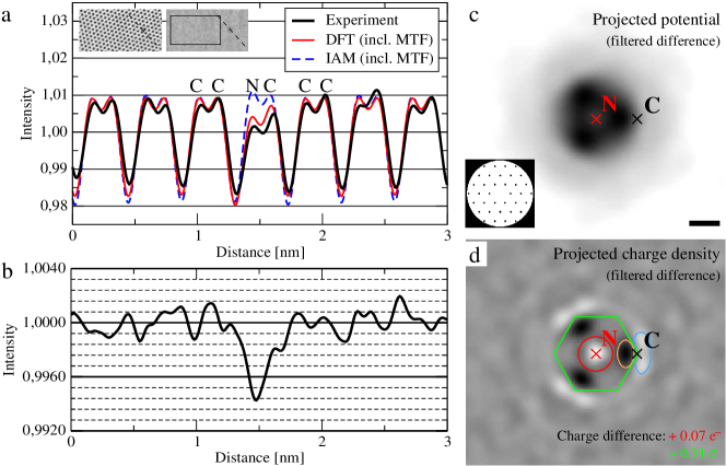
A quantitative comparison between the simulation and experiment is shown in Fig. 3. For this comparison, the modulation transfer function (MTF) of the CCD camera was measured and applied to the simulated images, following the procedure of Ref. ThustMTF09 . In addition, a small ( FWHM) gaussian blur was applied to both, unfiltered experimental data and simulation, in order to reduce the pixel noise in the experimental data. As can be seen in Fig. 3a, a good match of the experimental profile and the DFT based simulation is found. We then remove the periodic component of the graphene lattice, in order to estimate the noise level in this image. We obtain a standard deviation of 0.0008 in this case and a signal of the nitrogen substitution that is 7x above this noise (Fig. 3b).
While the TEM image depends directly on the electrostatic potentials, it is useful to look at both, the projected potentials and charge density of the calculations, in order to understand how the charges are re-arranged in the bonded configuration. Fig. 3c shows the difference in projected potentials, with the periodic components of the graphene removed (the unfiltered images are given in the supplement). Importantly, there is a spatially extended dark signal, with a diameter of ca. (twice the C-N bond length) in the projected potential. Fig. 3d shows the difference in projected charge densities, again with the periodic components removed. Here, one can see that the most dominant effect in the charge distribution is not on the nitrogen atom itself, but the dipole-shaped rearrangement of the electrons on the nearest-neighbour carbons around the nitrogen defect.
As a side remark, we note that the nitrogen defect is reactive NsubstDistAndCH05 , in comparison to the inert carbon surface. In some cases, we observe a repeated trapping and de-trapping of contamination atoms on the nitrogen defect in long image sequences (see supplementary information). The ad-atoms on the nitrogen defects are surprisingly stable, such that a few atomically resolved images can be obtained before the configuration changes under the beam. The reactivity of the nitrogen substitution might therefore be useful for the potential application of graphene as a TEM substrate, as it allows to trap objects while only minimally affecting its transparency.
IV Results and Discussion: Hexagonal Boron Nitride
We now turn to the calculations and measurements for the single-layer hexagonal boron nitride membranes. Hexagonal boron nitride (hBN) is a periodic structure with well known partially-ionic character PaulingBNandGrPNAS1966 . However, single-layer hBN membranes as obtained in a TEM are only a few nanometer in size MeyerBNnl09 ; IijimaBN09 ; ZettlHbn2009 ; KrivanekBNnature10 and therefore too small for an analysis by electron or x-ray diffraction. By using the direct image, we can choose a nanometer-sized area, which is in addition free of any defects.
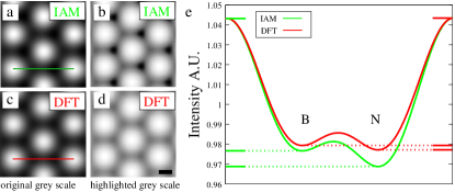
The conventional independent atom model (IAM) TEM simulation is shown in Fig. 4a+b, while Fig. 4c+d shows the TEM image simulation for the DFT based electrostatic potentials for the bonded configuration. The difference between the IAM and DFT model has important implications: The IAM based simulation predicts a significant contrast difference for the two elements, already with only (1-100 reflection) resolution. Thus, based on the IAM one would expect a different contrast for the B and N sites as soon as lattice resolution is achieved. The DFT based simulation, on the other hand, predicts a practically symmetric image in this case. It has to be considered as a coincidence that the elemental discrimination is not possible (at this resolution) when using the DFT based TEM simulation. We can interpret the DFT result in such a way that, due to the ionicity of h-BN, the contrast difference that is expected for neutral atoms is almost exactly canceled: The accumulation of electron charge on the N site, already noted by Pauling in Ref. PaulingBNandGrPNAS1966 , leads to a stronger screening of its core potential and thus a reduced contrast for this element (Fig. 4e, see also supplementary info). Thus, we can confirm the DFT prediction and verify the ionicity of single-layer hBN from HRTEM images, even though we can not assign the B and N sublattices.
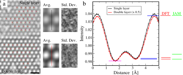
For the experimental case, the separation of intrinsic contrast (i.e., that of the sample) and effects of optical aberrations (from the microscope) is difficult and technical, and therefore discussed in more detail in the supplementary information. At this point, we only show the comparison between single-layer and bi-layer hBN. For a bi-layer, a symmetric profile is expected due to the symmetry of the projected structure (B is above N). Hence, any asymmetry in the bi-layer profile represents residual electron optical aberrations only. Assuming identical imaging conditions for all points of the sample, the comparison between a single-layer and bi-layer region would show the “intrinsic” contrast difference in the mono-layer, if present. The experimental result is shown in Fig. 5: Fig. 5a shows the direct image (average of 21 exposures), with 35 selected unit cells indicated in both areas, and their average and standard deviation. Fig. 5b shows the corresponding intensity profiles. Shown here as error bar is the standard deviation as mean deviation of individual unit cells from their average. The statistical uncertainty of the configuration average is again much lower (by a factor of ). Hence, statistical noise is not a significant source of error in these measurements.
However, the imaging conditions do vary across the field of view, and can easily differ already in regions separated by a few nanometer by an amount that is significant for this study. We describe in detail in the supplementary information how the variation of imaging conditions across the field of view can be measured for this particular material, and how differences in imaging conditions between single-layer and bi-layer reference are minimized. This degree of control for imaging conditions was not demonstrated in the previous HRTEM studies of this material IijimaBN09 ; ZettlHbn2009 . With a very high precision, the intensity profiles of the single-layer and double-layer hBN regions are exactly identical. We estimate an experimental error of 3% contrast difference between B and N (relative to the total modulation), based on comparisons of separated regions with the same thickness. This result is in agreement with the DFT calculation, but in contrast to the IAM prediction of 10% relative contrast difference. In other words, the ionic character of single layer h-BN is confirmed from a direct measurement, while the neutral-atom (IAM) charge distribution can be ruled out.
V General remarks and conclusions
As we have shown, details of the electronic configuration can be detected in high signal to noise ratio TEM images with carefully controlled conditions. One key ingredient is the fabrication of samples with precisely defined geometries DengMarksBonding06 , and a reduction of radiation damage in order to allow sufficiently high signal to noise ratios. Graphene and hBN are special in that they are easy to prepare in such well defined geometries, and maintain their crystalline surface configurations even under ambient conditions. We note that much larger chemical shifts than detected here have been predicted for a variety of materials in Refs. DengMarksBonding06 ; DengGlowingDefects07 , but could not be measured with common TEM sample preparation methods. The obvious implication is that one would need new ways of sample preparation and transfer, in order to study these effects in most other materials.
At the same time, our results also show that bonding effects have to be taken into account for structural and elemental analysis, in cases where small differences in elemental contrast are important. For example, based on the IAM one would assume that the identification of the B and N sublattices in hBN single layers is possible in bright-field high-resolution TEM images, already with resolution. However, based on the more accurate DFT potentials, one has to conclude that this is not possible. The experiment confirms this prediction, once instrumentation errors are suffiently well adressed. Hence, the question of which element forms the stable mono-vacancies in h-BN surfaces under TEM observation MeyerBNnl09 ; IijimaBN09 ; ZettlHbn2009 , remains unclear (a recent scanning-TEM study identified the two sub-lattices, but did not report the typical defects that are found in TEM observations KrivanekBNnature10 ). For the case of N doped graphene, the situation is quite different: Based on IAM, one would expect that a N substitution in graphene can not be detected. It is exclusively the effect of binding electrons that makes it possible to see nitrogen substitutions in graphene. Nitrogen substitutions in graphene - possibly beam-induced - also provide an alternative explanation to the weak dark contrast observed in Ref. MeyerAdatomsNat08 : The DFT based calculation predicts a ca. 0.6% dark contrast for the Scherzer image of the uncorrected microscope, in agreement with the observations (nitrogen substitutions had been ruled out based on IAM calculations with atomic configurations from the literature NsubstDistAndCH05 ; NsubstCNTbondlength07 ). As a further remarkable point, the contrast of the N defect is primarily due to a change in the electronic configuration on the neighbouring carbons, rather than on the nitrogen atom itself. Further, it is due to a higher moment (a dipole) in the charge on these atoms. Hence, it is also not possible to model these effects by using modified scattering factors for partly ionized atoms.
In conclusion, we have shown that it is possible to obtain insights into the charge distribution in nano-scale samples and non-periodic defects from TEM measurements with extremely high signal to noise ratios. For our examples of the nitrogen substitutions in graphene and hexagonal BN layers, we can assign experimentally observed features to details in the simulated electron distribution. We can detect a single light substitution atom in graphene, which is possible only due to an electronic effect. In the case of hBN, the charge redistribution leads to a loss of elemental contrast. Instead, the partial ionization of the material is experimentally confirmed for the single layer. One key ingredient here is the extraordinary stability of the samples under the low-voltage electron beam, which allows to obtain extremely high signal to noise ratios from long exposures. Further, the precisely defined, ultra-thin sample geometry enables a straightforward analysis. The DFT based TEM image calculation is irreplacable for the interpretation of experimental results in these materials, and can provide insights beyond the structural configurations.
Author contributions
J.C.M., A.C. and S.K. carried out TEM experiments. J.C.M., S.K. and A.C. analyzed the data. S.K. carried out DFT calculations and TEM simulations based on WIEN2k. A.C. contributed to TEM simulations, discussions, and analysis. H.-J.P., V.S., S.R. and J.S. developed the synthesis of N doped graphene. D.K. and A.G. carried out DFT calculations using VASP. G. A.-S. contributed to TEM simulations. T.I. and U. S. made Auger spectroscopy measurements. U.K. supervised part of the work. J.C.M. conceived and designed the study, and wrote the paper. S.K. and U.K. co-wrote the paper.
Acknowledgments
We gratefully acknowledge financial support by the German Research Foundation (DFG) and the Ministry of Science, Research and the Arts (MWK) of the state Baden-Wuerttemberg within the SALVE project and by the DFG within research project SFB 569. T.I. acknowledges the JSPS Postdoctoral Fellowship for Research Abroad. G.A-S. acknowledges the support of CONACyT-DAAD scholarship
References
- [1] E. J. Kirkland. Advanced Computing in Electron Microscopy. Plenum Press, New York, 1998.
- [2] P. R. Buseck, J. M. Cowley, and L. Eyring. High-Resolution Transmission Electron Microscopy. Oxford University Press, 1988.
- [3] T. Gemming, G. Mobius, M. Exner, F. Ernst, and M. Ruehle. Ab-initio hrtem simulations of ionic crystals: a case study of sapphire. J. Micr., 190:89, 1998.
- [4] S. Mogck, B. J. Kooi, J. Th. M. De Hosson, and M. W. Finnis. Ab initio transmission electron microscopy image simulations of coherent ag- mgo interfaces. Phys. Rev. B, 70:245427, 2004.
- [5] B. Deng and L. D. Marks. Theoretical structure factors for selected oxides and their effects in high-resolution electron-microscope (hrem) images. Acta Cryst. A, 62:208, 2006.
- [6] B. Deng, L. D. Marks, and J. M. Rondinelli. Charge defects glowing in the dark. Ultramicroscopy, 107:374, 2007.
- [7] J. M. Zuo, M. Kim, M. O’Keefe, and J. C. H. Spence. Direct observation of d-orbital holes and cu-cu bonding in cu2o. Nature, 401:49, 1999.
- [8] S. Shibata, H. Sekiyama, K. Tachikawa, and M. Moribe. Chemical bonding effect in electron scattering by gaseous molecules. J. Mol. Struct., 641:1, 2002.
- [9] D. Wei, Y. Liu, Y. Wang, H. Zhang, L. Huang, and G. Yu. Synthesis of n-doped graphene by chemical vapor deposition and its electrical properties. Nano Lett., 9:1752, 2009.
- [10] K. S. Novoselov, A. K. Geim, S. V. Morozov, D. Jiang, Y. Zhang, S.V. Dubonos, I.V. Grigorieva, and A.A. Firsov. Electric field effect in atomically thin carbon films. Science, 306:666, 2004.
- [11] A. K. Geim and K. S. Novoselov. The rise of graphene. Nature materials, 6:183, 2007.
- [12] J. C. Meyer, A. Chuvilin, G. Algara-Siller, J. Biskupek, and U. Kaiser. Selective sputtering and atomic resolution imaging of atomically thin boron nitride membranes. Nano Lett., 9:2683, 2009.
- [13] C. Jin, F. Lin, K. Suenaga, and S. Iijima. Fabrication of a freestanding boron nitride single layer and its defect assignments. Phys. Rev. Lett., 102:195505, 2009.
- [14] N. Alem, R. Erni, C. Kisielowski, M. D. Rossell, W. Gannet, and A. Zettl. Atomically thin hexagonal boron nitride probed by ultrahigh-resolution transmission electron microscopy. Phys. Rev. B, 80:155425, 2009.
- [15] O. L. Krivanek, M. F. Chisholm, V. Nicolosi, T. J. Pennycook, G. J. Corbin, N. Dellby, M. F. Murfitt, C. S. Own, Z. S. Szilagyi, M. P. Oxley, S. T. Pantelides, and S. J. Pennycook. Atom-by-atom structural and chemical analysis by annular dark-field electron microscopy. Nature, 464:571, 2010.
- [16] K. S. Kim, Y. Zhao, H. Jang, S. Y. Lee, J. M. Kim, K. S. Kim, J.-H. Ahn, P. Kim, J.-Y. Choi, and B. H. Hong. Large-scale pattern growth of graphene films for stretchable transparent electrodes. Nature, 457:706, 2009.
- [17] X. Li, W. Cai, J. An, S. Kim, J. Nah, D. Yang, R. Piner, A. Velamakanni, I. Jung, E. Tutuc, S. K. Banerjee, L. Colombo, and R. S. Ruoff. Large-area synthesis of high-quality and uniform graphene films on copper foils. Science, 324:1312, 2009.
- [18] H. J. Park, J. C. Meyer, S. Roth, and V. Skakalova. Growth and properties of few-layer graphene prepared by chemical vapor deposition. Carbon, 48:1088, 2010.
- [19] G. Kresse and J. Furthmüller. Efficient iterative schemes for ab initio total-energy calculations using a plane-wave basis set. Phys. Rev. B, 54:11169, 1996.
- [20] Daniela Künzel, Thomas Markert, Axel Groß, and David M. Benoit. Bis(terpyridine)-based surface template structures on graphite: a force field and dft study. Phys. Chem. Chem. Phys., 11:8867–8878, 2009.
- [21] P. Blaha, K. Schwarz, G. K. H. Madsen, D. Kvasnicka, and J. Luitz. WIEN2K: An Augmented Plane Wave and Local Orbitals Program for Calculating Crystal Properties. Vienna University of Technology, Vienna, Austria, 2001.
- [22] Z. H. Zhu, H. Hatori, S. B. Wang, and G. Q. Lu. Insights into hydrogen atom adsorption on and the electrochemical properties of nitrogen-substituted carbon materials. J. Phys. Chem. B, 109:16744, 2005.
- [23] S. H. Lim, R. Li, W. Ji, and J. Lin. Effects of nitrogenation on single-walled carbon nanotubes within density functional theory. Phys. Rev. B, 76:195406, 2007.
- [24] M. Lentzen. Progress in aberration-corrected high-resolution transmission electron microscopy using hardware aberration correction. Microscopy and Microanalysis, 12:191, 2006.
- [25] J. C. Meyer, A. K. Geim, M. I. Katsnelson, K. S. Novoselov, T. J. Booth, and S. Roth. The structure of suspended graphene sheets. Nature, 446:60, 2007.
- [26] J. C. Meyer, A. K. Geim, M. I. Katsnelson, K. S. Novoselov, D. Obergfell, S. Roth, C. Girit, and A. Zettl. On the roughness of single- and bi-layer graphene membranes. Solid State Communications, 143:101, 2007.
- [27] A. Thust. High-resolution transmission electron microscopy on an absolute contrast scale. Phys. Rev. Lett., 102:220810, 2009.
- [28] L. Pauling. The structure and properties of graphite and boron nitride. Proc. Natl. Acad. Sci., 56:1646, 1966.
- [29] J. C. Meyer, C. O. Girit, M. Crommie, and A. Zettl. Imaging and dynamics of light atoms and molecules on graphene. Nature, 454:319, 2008.
- [30] J. C. Meyer, C. O. Girit, M. F. Crommie, and A. Zettl. Hydrocarbon lithography on graphene membranes. Appl. Phys. Lett., 92:123110, 2008.
- [31] B. W. Smith and E. Luzzi. Electron irradiation effects in single wall carbon nanotubes. J. Appl. Phys., 90:3509, 2001.
- [32] John P. Perdew, Kieron Burke, and Matthias Ernzerhof. Generalized gradient approximation made simple. Phys. Rev. Lett., 77:3865, 1996.
- [33] P. E. Blöchl. Projector augmented-wave method. Phys. Rev. B, 50:17953, 1994.
- [34] G. Kresse and D. Joubert. From ultrasoft pseudopotentials to the projector augmented-wave method. Phys. Rev. B, 59:1758, 1999.
- [35] V. L. Solozhenko and T. Peun. Compression and thermal expansion of hexagonal graphite-like boron nitride up to 7 gpa and 1800 k. Journal of Physics and Chemistry of Solids, 58(9):1321 – 1323, 1997.
- [36] L.-M. Peng and J. Cowley. Errors arising from numerical use of the mott formula in electron image simulation. Acta Cryst. A, 44:1, 1988.
- [37] P. A. Doyle and P. S. Turner. Relativistic hartree-fock x-ray and electron scattering factors. Acta Cryst. A, 24:390, 1968.
- [38] P. Thévenaz, U.E. Ruttimann, and M. Unser. A pyramid approach to subpixel registration based on intensity. IEEE Transactions on Image Processing, 7(1):27, January 1998.
Supplementary information
VI Synthesis of N doped graphene
Nitrogen doped graphene is prepared by Chemical Vapor Deposition (CVD) with nickel (Ni) or copper (Cu) as a catalyst. It mostly follows the procedure which has been developed for pristine graphene and results in high quality graphene [16, 17] and graphene membranes [18], with the addition of ammonia as nitrogen source during part of the synthesis [9]. The experimental procedure for nitrogen doped graphene growth using both catalysts is same except reaction time (3 min for Ni and 20 min for Cu).
In detail, a Ni or Cu film with 300 nm of thickness was coated onto a substrate using an electron beam evaporator. The metal coated substrate was located on the middle of a quartz tube and heated to 1000 °C at a 40 °C/min heating rate, under a flow of argon (500 sccm) and hydrogen (500 sccm). The metal film on /Si was annealed further at 1000 °C for 20 min. A mixture of gases with a composition ( = 200:500:2500 sccm) was introduced at 980 °C for 3 min (Ni) or 20 min (Cu). Then, the sample was cooled down at a rate of ca. 6.7 °C/min. During cooling, ammonia was introduced instead of within the temperature range of 800 °C to 400 °C (introducing ammonia at higher temperatures destroyed the metal layers). The sample is then further cooled down to room temperature under Ar (200 sccm) and (500 sccm) flow. For transferring the doped graphene layers onto a TEM grid, poly(bisphenol A carbonate) (PC) was dissolved in chloroform (solid content : ~ 15 wt%). The PC/chloroform solution was spin-coated onto the graphene/metal//Si substrate with 500 rpm for 2 min. The PC was deposited onto the substrate homogeneously with ~10 m of thickness. The graphene/PC film was released free-stranding by chemical etching of the Ni layer with a (1 M) solution, followed by a concentrated HCl solution. The etching time varied depending on the substrate size from 30 min to 12 h. The graphene/PC film was rinsed several times with DI-water and dried with nitrogen gas. It was then placed onto the TEM grid, and the PC was dissolved using chloroform. Before inserting into the microscope, in order to further reduce adsorbed contamination, the TEM grid with graphene layer was heated in air to 200 °C for 10 minutes.
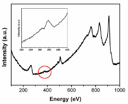
The presence of nitrogen in the doped samples was verified by Auger spectroscopy (Fig. 6). A small signal at the N KLL energy is found (enlarged as inset in Fig. 6), which is not present in undoped reference samples. The other lines in the spectra correspond to carbon, oxygen (presumably physisorbed after air exposure) and copper, and are also found in the undoped graphene reference samples. Auger spectroscopy was performed using a JEOL JAMP-7810 scanning Auger microprobe at 15keV.
VII Additional images for N doped graphene
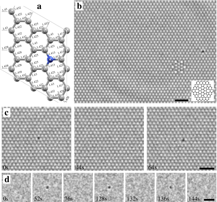
Fig. 7a shows the DFT relaxed configuration of N doped graphene as used in all simulations. Fig. 7b-d shows some additional observations from nitrogen doped graphene. Fig. 7b shows an example of an unexpected defect configuration that was frequently found in the nitrogen doped samples that were synthesized on the Ni surface. It consists of seven hexagons that are rotated by 30°, connected to the graphene lattice by six pentagons and heptagons. Due to its peculiar appearance we will refer to it as flower defect. Its formation mechanism remains unclear at this time. Remarkably, the flower defect is not a reconstructed vacancy; i.e., it contains the same number of atoms as the ideal graphene sheet.
We note that the nitrogen defect is reactive [22], at least in comparison to the inert carbon surface. Frequently, the nitrogen substitution defects have isolated ad-atoms trapped on top at the beginning of the observation, which then detach under electron irradiation after a few exposures and thus reveal the isolated nitrogen substitution defects. These ad-atoms are trapped on the nitrogen atom or its neighbouring carbons. In some cases, we observe a repeated trapping and de-trapping of contamination atoms on the nitrogen defect in long image sequences. The sequence in Fig. 7c is recorded at Scherzer defocus and shows direct structure images. An ad-atom is present initially, desorbs in intermediate images, and another ad-atom is again trapped in the same place (within one nearest neighbour). Sequence (d) is recorded at the larger defocus (-18nm, optimized for N substitution detection), the lattice is filtered out. Here, several events are observed where an ad-atom is trapped on the same position. Indeed, this dynamics provides an independent confirmation of the nitrogen defect in this position: The repeated trapping of ad-atoms in the same position (within one nearest neighbour) proves that there must be some kind of reactive defect within the single layer graphene sheet at this point. However, the intermediate frames appear identical to undisturbed graphene within the noise level of single exposures, which allows only substitutions of similar atomic number (B, N, O) as alternatives to carbon. Then, given the intentional presence of nitrogen during synthesis of these samples, we can identify these defects as nitrogen substitutions. For the nitrogen substitution analysis as shown in the main article, we have to use averages from several exposures. For this purpose, we only use parts of the image sequences where no ad-atom is visible in all individual exposures.
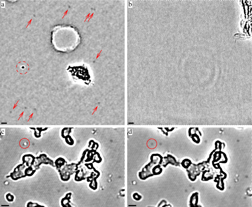
In Fig. 8 we show further TEM images of nitrogen substitutions in graphene. Fig. 8a,b shows the comparison of a nitrogen doped sample and an un-doped reference graphene sample. In this case, Fig. 8a shows a graphene sheet grown on a Ni surface in presence of ammonia, and Fig. 8b shows a graphene sample that was prepared by mechanical cleavage [30] (and not irradiated above the knock-on threshold [31]). Fig. 8c,d shows a sample that was also prepared by mechanical cleavage, briefly irradiated with 300keV electrons (with a dose of ca. ). The sample shown in Fig. 2i of the main article was left in the microscope vacuum between irradiation and imaging (ca. 2 hours later), while the sample in Fig. 8c,d was exposed to air. In both cases, we observe nitrogen substitution defects. A likely mechanism is a substitution of irradiation-induced vacancies by nitrogen atoms. Indeed, the sequence in Fig. 8c,d shows one example where a vacancy defect converts into a nitrogen substitution defect during observation. All images in Fig. 8 are averages of ca. 40 exposures, recorded at a defocus of and a gaussian low-pass filter was applied such that the graphene lattice is almost suppressed but still discernible. Also, we note in the larger-area views (Fig. 8a,b) that the imaging conditions are close to ideal only near the amorphous adsorbates that are used for fine tuning. The contrast of the nitrogen substitution is only weakly dependent on small residual non-round aberrations. Therefore, this topic is discussed in more detail below in the context of hexagonal boron nitride images, where it is important for the analysis.
VIII Details of the VASP DFT simulation
Spin-polarized DFT calculations were carried out with the Vienna ab initio simulation package (VASP) [19]. The structure of the substitution defects in graphene was relaxed using the exchange-correlation functional by Perdew, Burke and Ernzerhof (PBE) [32]. Ionic cores were represented by the projector augmented-wave (PAW) method [33, 34]. An energy-cutoff of 400 eV was used for the calculations. With these parameters, the pure graphene layer has a relaxed C-C-distance of 1.424 Å. For the calculations of the defect structure, a supercell of the hexagonal graphene unit cell was used (lattice constant: 9.868 Å). We employed a large k-point mesh with a Gaussian smearing of 0.1 eV for the k-point summation in order to ensure well-converged geometries of the considered structures. Different initial configurations with the nitrogen atom slightly displaced in different directions all resulted in the same relaxed structure. The relaxation process was stopped when all forces were smaller than 0.002 eV Å-1.
IX Details of WIEN2K DFT simulation
The all-electron WIEN2K DFT simulation is used to obtain the electron charge density and electrostatic potential, for a structure with fixed atomic coordinates. For boron nitride we use the literature value of [35] (separation between B and N atoms of ), and for nitrogen doped graphene we use the relaxed configuration described above (see Fig. 7a). We have evaluated the required number of k-points and size of the base set (RKMAX) by convergence tests. To this end, we have not only tested a convergence of the total energy and electric field gradient, but also of our value of interest, the projected potential values. For the results shown in the main article, we used 54 k-points with 15x15x3 division for the hBN results. For the nitrogen substituted graphene supercell, we used 8 k-points with 4x4x1 division and RKMAX=8. The muffin-tin radius is set automatically by WIEN2K to create spheres that touch with the nearest neighbours. All other values are left to the defaults of the WIEN2K software (version 9.1).
X Image simulation based on WIEN2K results
X.1 Overview
For the TEM image simulation, it is important that all electrons are included in the simulation, and not only valence electrons. For this reason, we extract the electrostatic potentials from the WIEN2K results. This software was also used by Deng and Marks in Ref. [5]. However, they used X-ray scattering factors calculated by WIEN2K and transformed them to electron scattering factors using a modified version of the Mott-Bethe formula [36], while we extract potentials directly from WIEN2K. The advantage of our approach is the simplicity and in principle the possibility to carry out multi-slice simulations (not needed for our samples), while the drawback is a very fine required sampling of the potential and associated high computing time. The WIEN2K software calculates the electrostatic potential created by all electrons and all core charges. This potential is stored in a file called case.vcoul and contains the Coulomb potential in a lattice harmonics representation and as Fourier coefficients. The utility program lapw5 can be used to obtain linescans and 2d slices of this potential file. A large number of 2d slices is then extracted to obtain the 3d potential. We then calculate the projected potential in the direction of view of the TEM (i.e., normal to the graphene or hBN layers), and simulate the effect of the microscope as described further below.
X.2 Electrostatic potentials
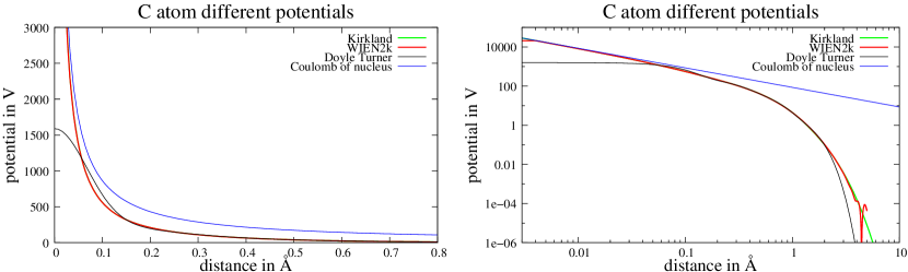
The aim of the next section is to clarify that the potential extracted from WIEN2K can be used directly for TEM image simulation. As a first test, we compare the results for an isolated atom with existing isolated-atom potentials. In Fig. 9 we see the comparison between the WIEN2K starting potential and two different isolated atom potentials by Doyle and Turner [37] and Kirkland [1]. The WIEN2K potential was obtained by defining a rectangular unit cell of with a single carbon atom inside. The starting charge density and the corresponding potential files were calculated and a linescan with a resolution of was created using the utility program lapw5. Far from the core the WIEN2K potential becomes constant but not zero. The linescans were shifted in z-direction (until the smallest value was equal zero) to obtain the WIEN2K potential in the common normalization. One factor that complicates this normalization is the fact that the WIEN2K potential starts to oscillate in the vacuum region, which is probably caused by the limited size of basis functions. However, the oscillations and deviations occur only in vacuum regions where the potential is very small and therefore do not affect our results. From the graphs in Fig. 9, we see that the WIEN2K and Kirkland potential agree very well in the core region where, in contrast to the Doyle Turner potential, both of them are divergent.
The excellent agreement of the isolated-atom potential from WIEN2K to the Kirkland potentials shows that the WIEN2K potentials are well suited for TEM simulation, and small changes from bonding should not affect this point. As a further useful fact, we found that the starting potentials from WIEN2K (i.e., results obtained with zero iterations of the DFT computation) are practically indistinguishable from the Kirkland potentials. In other words, the WIEN2K DFT simulation uses the independent-atom electron distribution as starting configuration. This provides an easy way to obtain an independent-atom (conventional) TEM simulation result for comparison with the DFT based result: Simulated images based on potentials extracted with zero iterations in WIEN2K correspond to the conventional (IAM) TEM simulation, while bonding effects are taken into account after the DFT based changes in the electronic configuration have been computed. In this way we can compare IAM and DFT results in a way that uses precisely the same algorithms and settings for modeling the effect of the microscope.
An important point that remains in working directly with the electrostatic potential in an equidistant 3-d grid is that we are making a discretization of a function that has poles at the positions of the nuclei. In this case, sampling points around the nucleus may not adequately represent the integrated potential of the corresponding volume element. In the extreme case, a sampling point may fall onto the position of the nucleus and thereby contribute an infinite value, multiplied with a finite volume element. To overcome this problem, we sample the electrostatic potential at a much higher spatial resolution than needed for image simulation, and use a global cut-off parameter for the potential to avoid infinite contributions. In other words, we mitigate the effect of the “bad pixel” at the position of the nucleus by using a very fine sampling, and subsequent averaging (this averaging or smoothing is inevitably part of the TEM simulation for the much lower realistic experimental resolution in the following step). Then, the main question is what sampling (points per Å) is needed, and how much error one has to expect as a result. To get an idea of the numbers, sampling at 30 points per Å and required (experimental) resolution of only means that there are volume elements within a cube, of which only one, which includes the nucleus, is affected by the cutoff. In this respect, it is important to note that the cut-off is implemented on the 3-D potential, and not the (2-D) projected potential which serves as input for the simulation.
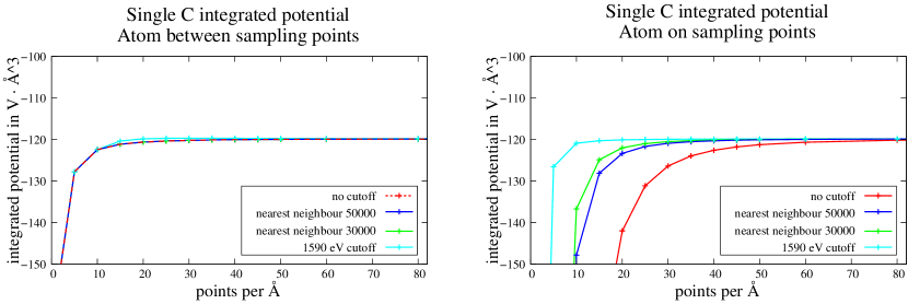
The required number of points is determined in a convergence test, where we use the integrated potential of the atom as the figure of merit. This is reasonable since, at the rather low experimental resolution (compared to the sampling in the simulation), only the integral value from the core region of the atom is relevant. In Fig. 10, we show the integrated potential for an isolated atom after extracting the potential with different sampling and different cutoff values. Also, the nucleus was placed onto the sampling point and in-between for comparison. As cut-off method, we use a nearest-neighbor cutoff, meaning that the potential value is reduced to that of the nearest pixel if it exceeds 30000 or 50000 volts, and a fixed cutoff of 1590V (maximum of the Doyle-Turner potential for carbon). If we use no cut-off, one would expect an infinite value if the atom is on the sampling point (an infinite value multiplied with a finite volume element numerically) but the maximum output value from lapw5 is (i.e., effectively another cutoff due to the numerical value range). Even with this extreme variation of values for the volume element that includes the nucleus, the integrated potential precisely arrives at for the highest sampling. In other words, the value of this one volume element does not matter if simply a sufficiently high sampling is used. The value is also in a very good agreement with the integrated potential from the Doyle-Turner parameters [37] of (which can be integrated analytically). Further, we can conclude that a sampling of 25-35 ppÅ is sufficient for our purposes if we use a reasonable cut-off algorithm. For the results presented here, we use a sampling rate of 104 ppÅ (hBN) and 52 ppÅ (N doped graphene unit cell) with the 50 kV nearest-neighbour cutoff.
As a further cross-check, we note again that we can obtain both the conventional (IAM) and DFT-based TEM simulation from the starting and final electron distribution in WIEN2K. For both cases, we use precisely the same sampling, integration, and positions of the nuclei with respect to the sampling points. Effects from poor sampling of the potential close to the nucleus, if present, would occur in both cases with the same magnitude (the positions of the nuclei are the same, and the electron charge density does not contain singularities). Hence, any sampling effects would show up in the comparison of our IAM result to other IAM simulation codes, based e.g. on Doyle-Turner potentials (which avoid the singularity), and this is not the case.
X.3 TEM image simulation
The previous section described how to obtain accurate electrostatic potentials on the atomic scale for a given structure in a way that includes the effects of chemical bonding. The first part of a TEM image simulation is now to model the effect of the sample on the electron beam. Since our samples consists of a single atomic layer, we use a single projection of the electrostatic potential. Then, the effect of the sample is simply a phase shift in the electron wave which is proportional to the projected electrostatic potential
where and is the wavefunction before and behind the sample, respectively,
is the projected potential, and the interaction parameter (where both electron mass and wavelength depend on the electron energy; is the electron charge, is the Planck constant). The projected potential is calculated numerically from the 3-D potential obtained from WIEN2K as described above.
The second part of the TEM image simulation is to model the effect of the microscope, which follows the standard approach as in Chapter 3 of Ref. [1]. We use a spherical aberration of 20m, an acceleration voltage of 80kV, a focal spread of 5nm, and a convergence angle of 0.5 mrad. The two defocus values are (Scherzer defocus) and (graphene lattice in the second extremum of the contrast transfer function (CTF)). The corresponding phase plates (including damping envelopes ) are shown in Fig. 11a,b. Experimentally, imaging conditions can be verified from the thin amorphous adsorbates that cover some parts of the graphene sheet. Fig. 11e,f shows the Fourier transform from such adsorbates, recorded in the same images and only a few nm away from our features of interest. For focus value , the single, continuous pass-band with the graphene lattice spacing at the outer rim is clearly visible in Fig. 11a,c,e. For focus value , a single dark ring in the power spectrum, just inside the graphene lattice spacing, is expected and confirmed in the experimental data (Fig. 11b,d,f).
XI TEM Data acquisition and processing
TEM imaging was carried out using an image-side spherical-aberration corrected Titan 80-300, operated at 80 kV, with the exception of Fig. 8c,d (50 kV) and Fig. 17 (100 kV). The extraction voltage of the source was reduced from its standard value (ca. 4 kV) to 2 kV, in order to obtain a lower energy spread. Images were recorded on the CCD camera (1k x 1k, Gatan MSC 742) or the CCD camera within the Gatan Imaging Filter (GIF), a 2k x 2k camera (Model US1000). The GIF camera was operated in a 2x binning mode in order to obtain a faster read-out; i.e. we were effectively using it as another 1k x 1k camera. In both cases, we use a sampling of 5 pixels per Angstrom (referring to the binned pixel size for the GIF camera).
Image sequences are recorded with ca. counts per pixel, 1 second exposure time, and ca. 2 second intervals. Effects of slightly uneven illumination are removed by normalization (division) to a copy of each image with a very large Gauss blur ( FWHM) applied. In this way, the long-range variations of the uneven illumination are removed, and at the same time the mean intensity is normalized to 1 throughout the image. The image data is upscaled to a 2x higher sampling ( pixel size) prior to image alignment, to avoid interpolation artefacts. Image registration is done with the Stackreg-plugin [38] for the ImageJ software, which provides sub-pixel accuracy for image alignment. In addition, Fig. 5a of the main article was rotated to be aligned with the crystal orientation.
XII Additional calculation results for nitrogen doped graphene
Although the TEM image depends directly on the electrostatic potentials, it is instructive to look at both, the projected potentials and the charge densities for IAM and DFT calculation. These two properties are related to each other via Poisson’s equation in the three-dimensional volume (however, note that we are showing the projected charge densities and potentials here). The difference between the IAM and DFT results shows how charges are re-arranged upon bond formation. Fig. 12a and b show a projection of the charge density, for the IAM and the DFT calculation, respectively. The change from a spherical charge distribution (IAM, Fig. 12a) to the charge distribution that is smeared out over the bonds (Fig. 12b) is apparent in the comparison of these two images. Fig. 12c shows the difference in the projected electron charge densities. In order to estimate a degree of ionization, it is necessary to define a volume surrounding each atom (i.e., an area in the projected charge density), and any choice here is of course arbitrary. First, we measure the excess charge on the nitrogen atom itself, by choosing a surface that cuts between the C and N atom (red circle in Fig. 12c). Here, the change is only as compared to a neutral atom (in agreement with a previous calculation [22]). Remarkably, the nitrogen atom itself is almost neutral and in fact is charged with the wrong sign to explain a dark contrast. Also, all carbon atoms are nearly neutral when choosing such a cylindrical boundary around the atoms. However, a hexagon shaped boundary through the nearest carbons (yellow in Fig. 12c) shows a difference of in this larger region (including the central circle). This reduced electron density, or positive net charge (reduced screening of the core potential) spread over a larger area, explains the smooth dark contrast associated to the nitrogen substitution. This charge is then mostly screened over a further atomic distance (blue hexagon). Further insight can be gained by removing the periodic components of this difference image, shown in Fig. 12d: From this image, it is clear that the most dominant effect is a dipole-shaped rearrangement of the electrons on the nearest-neighbour carbons around the nitrogen defect. Again, this delocalized charging effect agrees with the smooth appearance of the nitrogen defect in graphene as predominantly lower frequency components in the high-resolution experimental images. We can thus conclude that, in our experiment, the nitrogen substitution can be detected and appears the way it does mostly because of a charging effect on its neighbouring carbon atoms.
A similar analysis is shown for the projected potentials in Fig.12e-h. Here, the potential differences are given as relative differences (DFT-IAM)/DFT. In the comparison of the projected potentials, it should be noted that already for ideal graphene, the mean inner potential is reduced by 15% in the DFT result as compared to the IAM. The important insight here is that we obtain an extended region around the nitrogen defect where the projected potential is higher than in the surrounding graphene, visible in Fig. 12g,h as extended dark area.
XIII Additional calculation results for hexagonal Boron Nitride
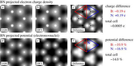
We analyze again both the projected potential and charge distribution, shown for hBN in Fig. 13. In the charge density, the change from a roundish (IAM, Fig. 13a) to a triangle-shaped distribution (DFT, Fig. 13b) is apparent in the comparison. Fig. 13c shows the difference in the projected electron charge densities. If we split the unit cell into two equal areas as indicated by the triangles in Fig. 13c, we find that 0.2 electrons shift from the boron to the nitrogen atom due to bonding (note that this value of partial ionization depends strongly on how these volumes are defined). In the projected potentials, we find that already the mean inner potential (the volume average of the potential) is 14% lower in the DFT result as compared to IAM (this difference might be detectable e.g. by electron holography). In the DFT result, the core potentials are screened over a shorter distance than in IAM, resulting in a slight reduction of atomic contrast and a sharper appearance of the atoms. However, this effect is stronger on the N site, leading to a practically cancelled contrast difference between B and N at our experimental conditions. The accumulation of charge on the nitrogen site is in agreement with the analysis of h-BN in the literature [28]. Again, the experimental TEM data confirms this ionic character of h-BN for the single layer, and rules out the neutral atomic configuration.
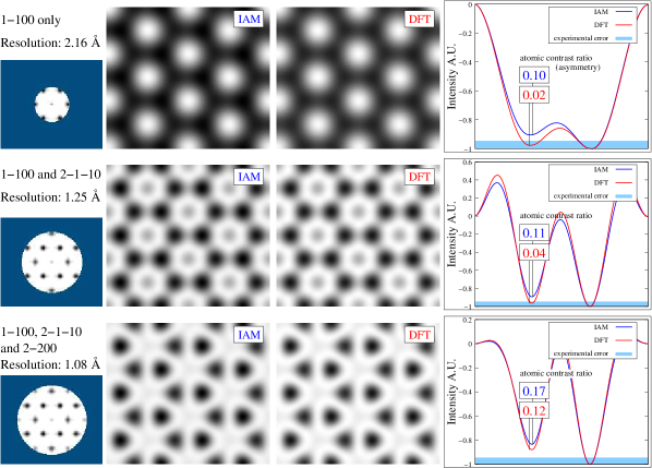
Based on the accurate electrostatic potentials from the all-electron DFT calculation, we briefly discuss the requirements for identifying the B and N sublattices in hBN single layer TEM images. For simplicity we show here the projected electrostatic potentials, limited to a specific resolution by apertures as indicated. In the real experimental case, the effect of the microscope would have to be modeled on top of this by an additional Fourier filter. However, at a given spatial resolution there can not be more information in the final image, than is already present in the projected potentials.
The analysis is very simple if only the first Bragg reflection (1-100, corresponding to ) is transferred. In general, the image of the hexagonal structure in this case is characterized by three values, the contrast on the three sub-lattices (B site, N site, hole in the hexagon). Further, the double-layer image can be used to verify the effects of residual aberrations. The IAM simulation with this aperture in Fig. 14 illustrates that it is in principle possible to have a different contrast for B and N sites at this resolution, even though the atomic separation is only . It has to be considered as a coincidence that the ionic character of the material leads to a practically symmetric contrast in the DFT based simulation. Importantly, our experiment confirms that no distinction between B and N sites is possible at this resolution, even with very high signal to noise ratio.
The situation is not changed by including the reflection into the image. This reflection can not carry any “which-atom” information already for symmetry reasons. It corresponds to a spacing in a hexagonal structure that adds the same contributions to the B and N sites (the relative numbers in Fig. 14 are slightly different due to the chosen normalization).
Only after including the (2-200) reflection, we expect a clear difference between B and N sites based on the DFT model. Also, the relative difference between IAM and DFT based simulation is smaller. This is reasonable, since at higher resolution there is more contribution from electrons scattered close to the nucleus, where bonding effects play a smaller role. Importantly, we note that a correct identification of B and N sites requires that the reflection (rather than just the as expected from IAM) is included into the image without any uncontrolled phase shifts. Hence, even if the beam could be transferred in an experiment (it corresponds to a scattering angle of 40mrad at 80kV), it is not obvious how one could separate the effects of electron optical aberrations from the intrinsic effect of the sample. As shown below, this is a complicated task already with only the first reflection, where one can use the bi-layer hBN regions as reference.
XIV Residual aberrations vs. intrinsic contrast
For the case of hexagonal boron nitride, it is important to verify and compensate the effects of residual, non-round aberrations. In thin hBN samples, it is frequently possible to find a “reference” structure for this purpose just next to the single-layer membrane, which is a region of double-layer hBN. For the bi-layer area, a symmetric contrast for the two sub-lattices must be present already due to the symmetry of the material (B is above N in adjacent layers). The asymmetry in the experimental intensity profiles for the bi-layer region therefore shows exclusively the effect of residual aberrations. In a simplistic approximation, one might assume identical imaging conditions for these different regions of the sample, imaged simultaneously and separated by a few nm. However, this has never been verified with a sufficient precision.
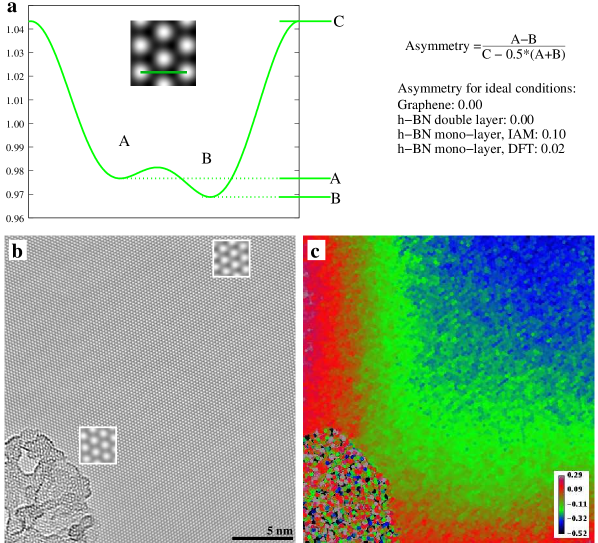
Fig. 15 shows a quantitative analysis of this point. We define an “Asymmetry” value as the relative contrast difference between the two atomic sites, normalized to the total modulation. Under ideal imaging conditions, a symmetric profile (Asymmetry of zero) would be expected for double-layer (or even-layered) hexagonal boron nitride regions, as well as for single-layer graphene. For single-layer hBN, one would expect an asymmetry of 0.10 from the independent-atom model, and 0.024 from the DFT based result. For triple-layer hBN, this relative asymmetry is expected as 0.033 from IAM, and 0.008 from DFT. Hence, it is also possible to discern between IAM and DFT from a single-layer - triple-layer comparison. We have implemented an automated method to measure this asymmetry for every unit cell (available as plug-in for the ImageJ software). The algorithm first locates all the intensity maxima, which represent the centers of the graphene or hBN hexagons. Then, it measures the intensity at these maxima (value C), as well as the intensity on the atomic sites A and B (at a given distance and orientation relative to the hexagon centers). As shown in Fig. 15, the asymmetry value does vary considerably over the field of view, as can be easily verified using images from large clean areas of single layer graphene.
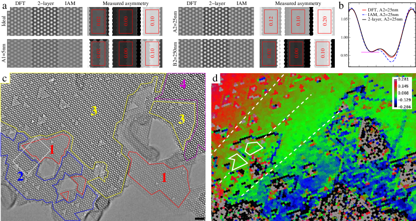
Now, we verify how the asymmetry for hBN depends on residual electron optical aberrations. We have tested all parameters up to third order aberrations. As examples, Fig. 16a shows simulated images for hBN in the presence of astigmatism (A1), two-fold astigmatism (A2), and coma (B2). As expected, the asymmetry depends on some of these values. However, the difference in the asymmetry from single-layer to bi-layer hBN is not sensitive to these effects. Thus, one would always expect a sharp step in the asymmetry value when going from (n) to (n+1) layers in hBN according to IAM, and almost no difference in the DFT model, independent of small residual aberrations.
Fig. 16b shows the intensity profiles for the example with a two-fold astigmatism of 25nm. Here, the bi-layer profile was rescaled by a factor of 1/2, and the left sublattice was shifted to the same position. We then compare the contrast on the other sublattice (as in the experimental analysis, Fig. 5 of the main article). We find that contrast difference in this comparison is the same as under ideal imaging conditions, independent of small non-round aberrations. Hence, the exact agreement between single-layer and (rescaled) bi-layer hBN, as found in the experiment, confirms the DFT model and rules out the IAM, independent of small residual aberrations.
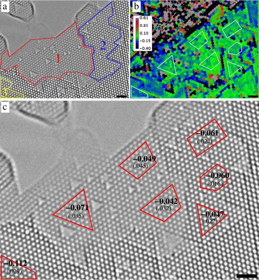
Fig. 16c shows the image of a larger area of ultra-thin hBN, with the image section that was used in the main article indicated by a white box. Fig. 16d shows the asymmetry measurement on the entire area. One can see a smooth trend from the top left to the lower right corner of the image, within large regions of constant thickness, which must be the effects of varying imaging conditions. The asymmetry value is unreliable at point defects, step edges, and in the vacuum region, which however are clearly discerned in the original image. The single- and bi-layer regions that were analyzed in the main article are again indicated (solid white lines). Based on the large-scale trend, these regions were chosen in a way that differences from residual aberrations are minimized. The white dashed lines indicate contours of approximately constant asymmetry, with the asymmetry values differing by 0.1. This corresponds to the IAM difference. As shown in Fig. 16b, a change in two-fold astigmatism of 25nm may produce this amount of asymmetry. However, the assignment to a specific aberration coefficient is not unique, and also not needed for the present analysis. In any case, one can easily obtain this 10% difference as an artefact if the variation of imaging conditions is not quantitatively verified, already with single-layer and bi-layer reference region separated by only a few nanometers.
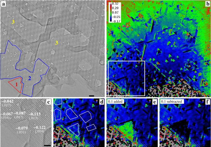
The automated analysis of the hBN images allows to verify our result for a larger amount of data, which would be very tedious when using manually selected and averaged unit cells. Fig. 17 shows an example measurement for the comparison of single-layer and bi-layer hBN using the automated asymmetry analysis. The automated analysis provides the asymmetry value on every individual unit cell. It is then easy to extract the mean value and standard deviation (in this example using 25 or more unit cells in each indicated area). The areas are chosen such that defects, step edges, and areas where the thickness has changed during the image sequence are avoided. The identical asymmetry in single- and bi-layer regions is confirmed. This means that the images are identical except for a constant factor in the total contrast. Also, several measurements in an area of constant thickness allow to further verify errors due to the variations in imaging conditions.
A further example is shown in Fig. 18. Fig. 18a+b show the larger scale image and the asymmetry analysis on the entire area. In one corner of the image (Fig. 18a), we find a single-layer area that is almost surrounded by a double layer that may serve as reference. We can now easily measure the asymmetry and its standard deviation for the mono-layer and all surrounding bi-layer areas: Fig. 18c shows the image section with the result of the asymmetry measurements, while 18d shows the color-coded asymmetry image along with the chosen areas. From all measurements, it is clear that there is no intrinsic difference; the image of mono-layer hBN is exactly identical to double layer hBN with half the contrast. All differences between separated regions are exclusively due to the variation of imaging conditions across the field of view. In this example, a difference of 0.1 is obtained over a spatial separation of ca. 7nm (the two furthest separated measurements in the bi-layer region, Fig. 18c, differ by 0.08), while several single-layer/double-layer comparisons can be made on a much shorter distance in the same image.
Indeed, the difference in asymmetry as predicted by IAM simulations should be detectable at the present noise level already from visual inspection of the asymmetry images. To demonstrate this, we have manually added and subtracted 0.1 to the asymmetry value of single layer regions (Fig. 18e,f): If the IAM prediction were correct, one would see such steps very clearly, and this is not the case in any of our measurements. Also, the step between single/triple, triple/double or triple/quad layer hBN should be well visible: It is only smaller in numerical value in our relative definition of the asymmetry but in this value also the noise is equally smaller in thicker sample areas. Again, the automated analysis allows to screen larger amounts of data, monitor the variation of imaging conditions with time (in image sequences), and makes possible errors that may arise in the manual analysis of a singular measurement highly unlikely.