Open quantum systems approach to atomtronics
Abstract
We derive a quantum master equation to treat quantum systems interacting with multiple reservoirs. The formalism is used to investigate atomic transport across a variety of lattice configurations. We demonstrate how the behavior of an electronic diode, a field-effect transistor, and a bipolar junction transistor can be realized with neutral, ultracold atoms trapped in optical lattices. An analysis of the current fluctuations is provided for the case of the atomtronic diode. Finally, we show that it is possible to demonstrate AND logic gate behavior in an optical lattice.
pacs:
05.10.Gg,05.30.Jp,05.60.Gg,67.85.-dI INTRODUCTION
The emerging field of atomtronics Micheli et al. (2004); Stickney et al. (2007); Pepino et al. (2009) aims to construct analogies of electronic components, systems and devices using ultracold atoms. In atomtronics, ultracold atoms move in an optical or magnetic potential in direct analogy with electrons moving in a semiconductor crystal. The motivation to construct and study atomtronic analogs of electronic systems comes from several directions.
First, the experimental atomtronic realizations promise to be extremely clean. Imperfections such as lattice defects or phonons can be completely eliminated. This allows one to study an idealized system from which all inessential complications have been stripped. Consequently, one may obtain an improved understanding of the essential requirements that make certain electronic devices work. It is possible that a deeper understanding may feed back to the design of conventional electronic systems and could lead to future improvements. This lies parallel to the recent interest in single electron transistors in mesoscopic systems Cardamone et al. (2005) and molecules Stafford et al. (2007), where many themes common with atomtronics emerge. A consequence of the near-ideal experimental conditions for optical lattice systems is that theoretical descriptions for atomtronic systems can be developed from first principles. This allows theorists to develop detailed models that can reliably predict the properties of devices.
Second, atomtronics systems are richer than their electronic counterparts because atoms possess more internal degrees of freedom than electrons. Atoms can be either bosons or fermions, and the interactions between atoms can be widely varied from short to long range and from strong to weak. This can lead to behavior that is qualitatively different to that of electronics Theis et al. (2004); Inouye et al. (1998, 2004); Stan et al. (2004). Consequently, one can study repulsive, attractive, or even non-interacting atoms in the same experimental setup. Additionally, current experimental techniques allow the detection of atoms with fast, state-resolved, near unit quantum efficiency Bakr et al. (2009). Thus it is possible, in principle, to follow the dynamics of an atomtronic system in real time.
Third, neutral atoms in optical lattices can be well-isolated from the environment, reducing decoherence. They combine a powerful means of state readout and preparation with methods for entangling atomsMandel et al. (2003). Such systems have all the necessary ingredients to be the building blocks of quantum signal processors. The close analogies with electronic devices can serve as a guide in the search for new quantum information architectures, including novel types of quantum logic gates that are closely tied with the conventional architecture in electronic computers.
Fourth and finally, recent experiments studying transport properties of ultracold atoms in optical lattices Strohmaier et al. (2007); Henderson et al. (2006); Denschlag et al. (2002) can be discussed in the context of the atomtronics framework. In particular, one can model the short-time transport properties of an optical lattice with the open quantum system formalism discussed here.
In this article we present a derivation of the master equation used to treat these specific open quantum systems. Afterward, we provide a detailed analysis of atomtronic analogies of the most elementary electronic components. These include conducting wires, diodes, and transistors. This work builds on a previous paper Pepino et al. (2009), providing a comprehensive explanation of the underlying analytical and numerical methods, and additional analysis of the components. Finally, we propose how AND logic gate behavior can be recovered in this open quantum system setting.
This article is organized as follows. In Sec. II we discuss the general master equation formalism, introducing the specific systems to be investigated, the defining properties of the reservoir, and the appropriate approximations necessary to complete the derivation for the models. In Secs. III and IV we apply the derived model to a variety of one-dimensional optical lattice systems in different open quantum system settings. The result is a collection of atomtronic devices that emulate electronic components.
II MODEL
II.1 System
Unlike the typical behavior of their electronic counterparts, atomtronic devices operate at the few-particle level. The necessary repulsive correlations between particles are generally caused by either strong interactions for bosons, or quantum statistical effects due to the Pauli exclusion principle for fermions. In this article we focus on bosonic current carriers, partly to draw contrast to the electronic case.
The optical lattice provides a clean, controllable environment for atomtronics components. Strong atom-atom interactions can be precisely tuned if the atoms are confined in a tight optical lattice. Holding the atoms in a lattice has two primary advantages. First, the strength of the interactions is enhanced due to the confinement within the lattice wells and second, by cooling the atoms deep into the lowest Bloch band regime, the center of mass motion of the atoms can be reduced to hopping between neighboring lattice sites. This results in a simple theoretical description as well as a clean experimental realization.
The dynamics of these ultracold atoms in this regime are accurately described by the Bose-Hubbard model Jaksch et al. (1998); Greiner et al. (2002). In the lowest Bloch band, the Bose-Hubbard Hamiltonian is
| (1) |
where and are lattice site indices, is the total number of lattice sites, is the site energy, is the on-site interaction energy, is the hopping energy, the sum is taken between adjacent lattice sites, and . Here, and are bosonic creation and annihilation operators respectively for an atom in the lowest Wannier orbital centered at site . Due to the precise tunability of the experimental parameters, , , and in the laboratory today, we use the Bose-Hubbard Hamiltonian to model our custom lattice atomtronic systems.
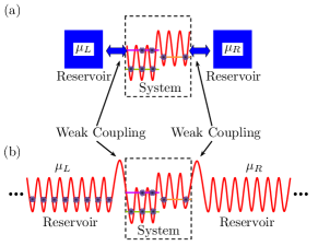
II.2 Reservoir
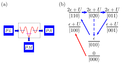
The reservoirs serve two purposes in atomtronics: they are ‘sources’ and ‘sinks’ of particles. The reservoirs themselves could be experimentally realized in a variety of different ways. For instance, a reservoir ‘source’ of atoms could be a 1-dimensional optical lattice (Fig. 1), or a strongly-interacting harmonically trapped ultracold gas. A reservoir ‘sink’ of atoms could be a coupling of the system to vacuum modes of atoms in an untrapped state or the densely spaced modes of a nearly empty potential well. For modeling purposes, suitable reservoirs must meet several requirements. The system-reservoir correlations must decorrelate from the system faster than the time scale over which the state of the system changes appreciably. This allows one to make the Markov approximation. We will also assume that system and reservoirs are weakly coupled so that we can make the second-order Born approximation. In order for the reservoirs to serve as incoherent sources of atoms, their density of states must vary slowly over the spectrum of the system.
In the model used in this work, it is assumed that the reservoirs are strongly-interacting bosons and at low temperatures, the states in the reservoir are filled to the chemical potential, and all states above the chemical potential are empty. This is analogous to the situation in a semiconductor crystal, where to a good approximation the electrons occupy all states up to the Fermi energy. Labeling the single particle excitations of the reservoir by a quantum number , we can write the Hamiltonian of the reservoir as
| (2) |
where and are the energy and creation operator for the ’th reservoir mode, respectively.
Such a reservoir can be constructed out of bosons trapped in a deep optical lattice potential. If the interactions between the atoms are very strong the system enters the Mott-insulator regime and by adjusting the chemical potential one can achieve a situation were each lattice site is occupied by precisely one atom. The atoms in this system could then be coupled to the atomtronic device to furnish an incoherent source of particles, as depicted in Fig. 1. By arranging the distribution of the energies in the reservoir it is possible to achieve a situation reminiscent of the Fermi-sea reservoir. We may then represent the reservoir by a collection of uncoupled harmonic oscillators.
II.3 Elimination of the reservoir: master equation formulation
The quantum master equation approach is often used in quantum optics for describing open quantum systems Cohen-Tannoudji et al. (1992); Meystre and Sargent (1999); Walls and Milburn (1994); Zubarev et al. (1997). In essence, it allows one to calculate observables associated with the evolution of a closed system without having to account for the free evolution of the reservoir. In this section we provide a detailed derivation of the master equation formulation for the system and reservoir described above. The derivation involves deriving an equation of motion for the reduced density operator for the system. Here we construct this equation of motion in a Liouville representation, since (as we discuss below) this form makes clear a way to go beyond the Born approximation, a necessity in this zero-temperature, unconventional setting.
The coupling of the system to the reservoir is by means of the exchange of particles between the system and the reservoir. The Hamiltonian for this interaction is
| (3) |
where is the annihilation operator for a particle in a system lattice site and is the coupling matrix element between reservoir mode and site .
The Hamiltonian for the system-reservoir interaction is given by
| (4) |
where for our model. For each part of the Hamiltonian we introduce an operation , defined by its action on an arbitrary operator by
| (5) |
We denote the density matrix of the system and reservoir with . From the full density matrix, the reduced density matrices and of system and reservoir are defined by tracing over the reservoir and system Hilbert spaces, respectively,
| (6) |
We define the projection operator by
| (7) |
and its compliment by . Under these definitions, and satisfy the usual projection operator relationships , , and . Using the projection operators, the reduced density matrix for the system can be written as
| (8) |
To find the equation of motion for , we start from the evolution of the full density matrix :
| (9) |
where . Noting that , this equation can be written as
| (10) |
Acting with and separates this equation into the coupled equations
| (11) | |||||
| (12) |
The solution of equation (12) is
| (13) |
where we have assumed that the system and reservoir initially uncorrelated, i.e. . Using this result to eliminate in Eq. (11) yields
| (14) |
Tracing over the reservoir Hilbert space leads to the equation of motion for the reduced density operator of the system,
| (15) |
where we have introduced the memory kernel
| (16) |
The first term on the right hand side of Eq. (15) is the free system evolution while the second term describes the irreversible contribution due to the system-reservoir interaction.
Equation (15) is the exact master equation under the condition that the system and reservoirs are initially uncorrelated. It achieves our goal, in principle: all the dynamics due to the coupling to the reservoirs is encapsulated in . Once the memory kernel is known we can calculate the evolution of the reduced density matrix of the system without having to take into account the reservoirs explicitly. However, it turns out to be impossible to solve for the memory kernel exactly in even the simplest of circumstances, so approximations must be made to continue from this point.
Calculation of the memory kernel and its action on the system density matrix is straight forward under the Markov and Born approximations. The Markov approximation assumes that the correlation time between system and reservoir is much shorter than the time scales over which the reduced density matrix of the system changes appreciably, i.e.
| (17) |
The Markov approximation consists of treating the system density matrix as a constant over time intervals of order , and accordingly we can pull it out of the integral in Eq. (15). The short correlation time also allows us to extend the limit of integration in Eq. (15) to infinity.
The Born approximation takes the memory kernel to second order in and is thus a weak coupling approximation. In the conventional Born approximation, is eliminated from the exponential term in the memory kernel. We cannot simply employ such an approximation here however since we are assuming that the strongly-interacting boson gas obeys a zero temperature Fermi-Dirac distribution characterized by . The hard edge at the Fermi energy causes logarithmic divergences in the second-order energy shifts of system levels as approaches system resonances. This divergence is due to the fact that, under the second-order approximation, as approaches a system resonance, the number of reservoir modes that the system is coupled to goes to one—not a continuum of modes. This would induce Rabi flopping of the atom between the system and the reservoir and not the irreversible reservoir action intended. In reality, the interaction of the system with the reservoir taken to all orders mixes the modes and leads to decay, in this situation. Exact simulations on small systems show that we can recover the proper dynamics at the hard edge by including the influence of higher order terms of the memory kernel expansion in . We find that the fourth order term in the expansion provides a good estimate for the higher order corrections of the full memory kernel, yielding
| (18) |
where . The evaluation of the fourth order term shows that the decay has a small dependence on the value about the system eigenenergy difference. Here, we take to be the mean value of the decay rate, which is where equals the system eigenenergy difference, that is , where is the density of reservoir modes, assumed to be constant in the region of interest. Introducing the rate at which particles enter or leave the system , we have . Taking this value for is reasonable because is only important in the calculation for only small deviations. The modified memory kernel in Eq. (18) captures the correct long-time behavior of the exact memory kernel.
With these approximations the master equation becomes
| (19) |
Inserting the Liouvillians into Eq. (19) yields
| (20) |
where we have used that
| (21) |
due to the fact that the reservoir is in thermal equilibrium.
We project Eq. (20) onto the energy eigenbasis of the system and trace out the reservoir degrees of freedom. This allows us to evaluate the integral and to find a more explicit form of the master equation. Given two arbitrary system energy eigenstates and and adopting the notation , we have
| (22) |
with being the difference between the eigenenergies of and . Similarly,
| (23) |
for the reservoir. Performing the integral over produces the following closed form of the master equation:
| (24) | |||||
where
| (25) | |||||
| (26) |
Note that
where indicates that integrals are to be interpreted in the Cauchy principal value sense. The real parts of the matrices then give decay rates that agree with the Fermi golden rule result while the imaginary parts give rise to level shifts in analogy with the Lamb shift in the hydrogen spectrum.
II.4 Reservoir model
The detailed physics of the reservoirs influence the evolution of the system through the coupling matrix elements , the occupation probabilities of the reservoir modes , and the density of states of the reservoir. The reservoir model used below assumes fermionized strongly-interacting bosons. Thus, for all modes below the chemical potential of the reservoir and for all modes above. The coupling of the reservoir modes to the system states is a slowly varying function of the mode energy. We model it by a constant coupling up to some high energy cut-off in order to quench the ultra violet divergence that would otherwise arise, taking the form,
| (27) |
with the Heaviside step-function. The high energy cut-off is much larger than any relevant frequency of the system, and it does not affect the system’s dynamics.
III ATOMTRONICS APPLICATIONS
In order to analyze the response of specific optical lattice configurations connected to reservoirs with different chemical potentials, we consider the steady-state solution of Eq. (24) and then proceed to solve for the matrix elements . Once is known, expectation values of atomic currents into (and out of) a system site can be calculated from reservoir’s influence of the system population rates. For the population of each state, we sum up net rates out of the system state and then subtract the net rates into the state. We then sum over all of the system states to obtain the net current transport on system site :
| (28) | |||||
| (29) | |||||
| (30) |
where
| (31) |
as the current operator for site projected onto the system eigenbasis. Using this convention, the sign of reveals whether the current flows into () or out of () the system.
III.1 Atomtronics analogy of a simple circuit
Here we analyze the atomtronics counterpart to a simple circuit of a battery connected to a resistive wire.

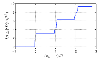
As seen in Fig. 2, the analogy of a wire is an energetically-flat optical lattice, with uniform tunneling rates and interaction energies ( , , and for all neighboring sites). For this system, that is very weakly-coupled to the reservoirs, we calculate the atomic current as a function of chemical potential difference. This numerical experiment is carried out by initially setting both left and right chemical potentials ( and ) to zero. We raise so that an atomic transport is induced across the system from left to right, we compute the current out of the right side of the system shown in Fig. 3. The current increases with the chemical potential difference, but in quantized jumps that correspond directly to the left chemical potential overcoming the on-site interaction energy needed to introduce a greater number of atoms onto the left site. A closer examination of the numerical simulation implemented in Fig. 3 reveals two subtle features. Moving from left to right across graph in Fig. 3, the first current jump, occurring at , the current increases in two steps where one might expect to observe a single jump, since the condition to put a particle in the lattice is . This is a result of the fact that the degeneracy of the Fock states in the one-particle manifold are split by in the system state eigenbasis. In addition the jump in current is broadened slightly by the nonzero and the system-reservoir coupling. This broadening, which makes the jump in current a smooth transition is more apparent in the atomtronic devices presented below where the system reservoir-coupling is taken to be orders of magnitude larger. Although the exact details for the second and third jumps are more complicated, the reasoning is the same: the eigenenergies are split by approximately , and the overall jump is smoothed out by . These are general properties of all of the numerical experiments described in this work.
III.2 The atomtronic diode
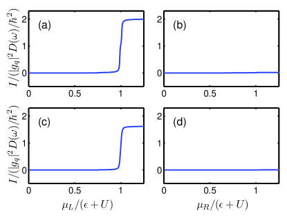
A diode is a device with an approximately unidirectional current characteristic. A voltage bias across the diode yields a current in one direction but not in the opposite direction if the voltage bias is reversed. Such behavior can be realized in an optical lattice by creating an energy shift in half of the lattice with respect to the other. We find that the diode characteristic persists as the number of lattice sites is increased. For simplicity, here we present the diode in a two-site lattice system. For the simulations in the rest of this paper, we assume , , .
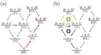
In the Fock basis for a two site system, there exist three states in the two-particle manifold: , , and , where refers to particles on the left site and particles on the right. The external energies of the two sites ( and ) can be chosen so that the eigenstates and approximately degenerate, leaving both states far detuned from . This configuration of the site energies is given by . We refer to this as the “resonance condition”.
Figure 4 illustrates how the resonance condition generates reverse-bias and forward-bias behavior in a two-site optical lattice. As seen in Fig. 4(a), if one holds the left reservoir chemical potential at and raises the right reservoir chemical potential , the system will undergo a transition from to . The states and are separated in energy by . As a result, most of the population remains in the state. Increasing above the point where the transition from to is allowed, the system remains almost completely settled in the state.
As seen in the Fig. 4(b), if one holds and raises , the system first undergoes a transition from to . However, increasing so the system evolves to leads to a very different situation than in the above case: since is resonant with , both states are simultaneously populated. Since takes all particles out of the site on the right, the system can make a transition from back to . The combined effect of setting and to these values is to force the system to undergo a closed cycle of transitions between , and . The result is a net atomic transport (or current flow) across the system. A second contributor to the net current through the system is the fact that allows transitions from to . Thus, an additional current-generating cycle exists: to to and back to . Both cycles contribute positively to a net current flow across the system.
For systems consisting of lattice sites, the diode configuration consists of two connected, energetically-flat lattices whose energy separation is . The dynamics do not change for larger systems since the degeneracy of the flat lattice allows for effective transport across the lattice, allowing a particle to enter the left site of the half of the lattice is energetically degenerate with finding a particle at the junction. Thus, there exist current cycles initially generated from the to transition. Going the other direction, one can go to , but conditions are not energetically favorable to allow atomic transport across the junction. Figure 5 is a schematic of a four-site atomtronic diode in the forward-biased direction.
Supporting the behavior that the dynamics of the diode are qualitatively-independent of the overall size of the lattice, Figs. 6(a-b) and 6(c-d) are numerical simulations of the current responses of the two site, and four site diodes, respectively. The general features of both diodes are qualitatively identical.
Given the current characteristics of the diode, one might ask how much does the signal fluctuate. Recalling the current operator from Eq. (31), we can calculate the autocorrelation function for the current,
| (32) |
using the quantum regression theorem.
To simulate an actual measurement, we convolve this correlation function with an exponentially decaying filter, . The Fourier transform of this convolution yields a time-averaged spectral density function . Our time-averaged signal-to-noise ratio SNR as a function of is then
| (33) |
For long averaging times we find, for the conditions of Fig. 6,
| (34) |
For typical optical lattice experiments, is achievable, which implies that . Therefore, a signal-to-noise ratio of can be achieved by averaging the atomic current for about second.
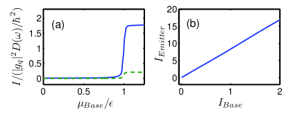
III.3 The atomtronic field-effect transistor
A field-effect transistor (FET) is a device that allows an externally-applied field to affect the current through the device. This characteristic allows the FET to be utilized as an amplifier. Since the diode is optimized when the resonance condition is imposed on the optical lattice, small deviations from the resonance condition lead to large changes in maximum current propagating across the lattice. This is precisely the behavior of a FET where a current is controlled by an applied voltage. In Fig. 7, we plot several current results for the forward-bias configuration as the separation in the external energy of the second site is raised past the resonance condition by fractions of , the smallest system parameter in the model.

III.4 The atomtronic bipolar junction transistor
A bipolar junction transistor (BJT) is a three terminal device in which the overall current across the emitter and collector is controlled by a much weaker current via the base. Two practical applications of the BJT are signal amplification and switching (on and off) of the emitter current.
Realization of BJT-like behavior in atomtronic systems requires at least three sites connected to three different reservoirs. If the atomtronic diode is considered an atomtronic p-n junction, one might guess that the atomtronic n-p-n transistor would entail raising the external energy of the left and right (collector and emitter) sites higher than the middle (base) site by the on-site interaction energy. This configuration is illustrated in Fig. 8(a).
The reason this configuration yields BJT-like behavior is due to the approximate degeneracy between the Fock states , , and .
We implement numerical simulations of this lattice configuration by fixing a chemical potential difference across the lattice. The left reservoir chemical potential is set to maintain one particle on the left site and the chemical potential of the right reservoir is set to zero. The middle chemical potential starts at zero and is increased to allow a single atom to enter the middle site.
When there are no atoms on the middle site, the configuration of the reservoirs pumps the system into the Fock state (as seen in Fig. 8(b)). The and the states are degenerate with each other, but the system must undergo a second-order, off-resonant transition via the state from to . Such transitions are suppressed by a factor of and thus become less likely as the energy difference between and increases. Thus, when the middle reservoir is set to maintain zero atoms on the middle site, the net current out of the emitter is minimal.
When the middle reservoir’s chemical potential is increased to allow a single atom into the middle site of the system, the degeneracy between the , , and states is accessed, which allows atoms to travel across the system. One issue with this configuration is the following: in order to get to , the system has to make a transition through the state. Since the middle reservoir is set to maintain an occupancy of one, but not two, atoms on the middle site, one of the atoms can be lost to the middle reservoir, leading to a loss of current out of the emitter. If the couplings of all three reservoirs to the system are equal, then the result is the current measured passing through the base turns out to be even greater than the current measured out of the emitter. Thus, the system represents an inefficient transistor realization. On the other hand, if the middle reservoir were to be coupled weakly compared to the other reservoirs, then current predominantly leaves the system via the emitter, which is the desired behavior.
Figure 9(a) is a numerical simulation of the current out of the emitter and the base as a function of the base chemical potential. The coupling strength of the base connected to the reservoir is one fifth the collector and emitter reservoir coupling. It should be noted that the region where the proposed atomtronic transistor mimics the electronic BJT is limited to the transition region, or current jump. One can increase the length of this region by increasing the overall system-reservoir coupling strength. Figure 9(b) shows that the gain of this device is fairly linear.
IV DISCRETE ATOMTRONICS LOGIC
Integrated circuits are designed with a very large number of transistor elements to perform a desired function. The demonstrated ability to realize atomtronic diodes and transistors thus motivates the question as to whether higher functionality can be realized with these ultracold atomic systems. Here we look at the most fundamental of these, the atomtronic AND logic gate.
A traditional logic element is a device with a given number of inputs and outputs, composed of switches, that generates a series of logical responses. Such logical behavior can be expressed in a truth table composed of ’s and ’s (‘ons’ and ‘offs’). Logic elements are the fundamental building blocks of computing and discrete electronics. In table 1(a) the truth table for the AND logic gate is given as an example. The next level of complexity in emulating electronic systems is to create logic elements from the atomtronic components.
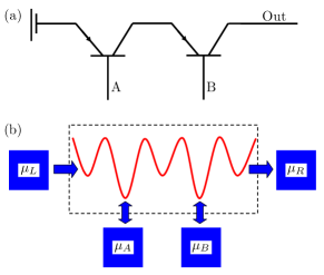
An AND gate is a device with two inputs ( and ), and one output (). As illustrated in table 1(a), the device characteristic of the AND gate is that remains off unless both and are on. In electronics, such a device can be constructed by connecting two transistors in series (as illustrated in Fig. 10(a)). By analogy, if the atomtronic BJTs are connected in the same series configuration (as illustrated in Fig. 10(b)), the AND gate truth table can be generated.
When constructing practical logic circuits, the values of the s and s are not strict values, they are defined within a given range. The data in table 1(b) has been generated in a numerical experiment of the configuration depicted in Fig. 10(b). For this particular experiment, the maximal current out of the device is at least a factor of greater than any other measured current out. Thus a discernible difference between ‘on’ and ‘off’ is observed and the output currents reproduce the AND gate truth table. Such a difference can also be enhanced by increasing the on-site interaction energy of the lattice.
| (a) | ||
| AND Gate | ||
| 0 | 0 | 0 |
| 1 | 0 | 0 |
| 0 | 1 | 0 |
| 1 | 1 | 1 |
| (b) | ||
| Atomtronic AND Gate Simulation | ||
V CONCLUSIONS
In this article, we have derived a general model for treating a specific class of open quantum systems where the reservoirs act as sources and sinks for particles moving into and out of the system. Such a formalism can be used to study atomic transport across arbitrary multiple potential well configurations. Here, the formalism was used to show how neutral atoms in custom optical lattices can exhibit electronic diode, FET, BJT, and AND gate behavior.
Looking forward, we aim to develop more complicated atomtronic devices such as additional logic elements, flip-flops, and constant current sources by cascading our current atomtronic components in a manner analogous to the development more sophisticated electronic devices. The simulation of the AND gate is promising since it demonstrates the possibility of cascading atomtronic components to make more sophisticated devices.
VI ACKNOWLEDGMENTS
We would like to thank Rajiv Bhat, Brandon Peden, Brian Seamen, and Jochen Wachter for their helpful discussions. This work was supported by AFOSR and NSF.
References
- Micheli et al. (2004) A. Micheli, A. J. Daley, D. Jaksch, and P. Zoller, Phys. Rev. Lett. 93, 140408 (2004).
- Stickney et al. (2007) J. A. Stickney, D. Z. Anderson, and A. A. Zozulya, Phys. Rev. A 75, 013608 (2007).
- Pepino et al. (2009) R. A. Pepino, J. Cooper, D. Z. Anderson, and M. J. Holland, Phys. Rev. Lett. 103, 140405 (2009).
- Cardamone et al. (2005) D. M. Cardamone, C. A. Stafford, and S. Mazumdar, Nano Lett. 6, 2422 (2006) (2005).
- Stafford et al. (2007) C. A. Stafford, D. M. Cardamone, and S. Mazumdar, Nanotechnology 18, 424014 (2007).
- Theis et al. (2004) M. Theis, G. Thalhammer, K. Winkler, M. Hellwig, G. Ruff, and R. Grimm, Phys. Rev. Lett. 93, 123001 (2004).
- Inouye et al. (1998) S. Inouye, M. R. Andrews, J. Stenger, H.-J. Miesner, D. M. Stamper-Kurn, and W. Ketterle, Nature (London) 392, 151 (1998).
- Inouye et al. (2004) S. Inouye, J. Goldwin, M. L. Olsen, C. Ticknor, J. L. Bohn, and D. S. Jin, Phys. Rev. Lett. 93, 183201 (2004).
- Stan et al. (2004) C. A. Stan, M. W. Zwierlein, C. H. Schunck, S. M. F. Raupach, and W. Ketterle, Phys. Rev. Lett. 93, 143001 (2004).
-
Bakr et al. (2009)
W. Bakr,
J. Gillen,
A. Peng,
S. F
”olling, and M. Greiner, Nature 462, 74 (2009). - Mandel et al. (2003) O. Mandel, M. Greiner, A. Widera, T. Rom, T. W. Hänsch, and I. Bloch, Nature (London) 425, 937 (2003).
- Strohmaier et al. (2007) N. Strohmaier, Y. Takasu, K. Gunter, R. Jordens, M. Kohl, H. Moritz, and T. Esslinger, Phys. Rev. Lett. 99, 220601 (2007).
- Henderson et al. (2006) K. Henderson, H. Kelkar, B. Gutiérrez-Medina, T. C. Li, and M. G. Raizen, Phys. Rev. Lett. 96, 150401 (2006).
- Denschlag et al. (2002) J. H. Denschlag, J. E. Simsarian, H. Haeffner, C. McKenzie, A. Browaeys, D. Cho, K. Helmerson, S. L. Rolston, and W. D. Phillips, J. Phys. B 35, 3095 (2002).
- Jaksch et al. (1998) D. Jaksch, C. Bruder, J. I. Cirac, C. W. Gardiner, and P. Zoller, Phys. Rev. Lett. 81, 3108 (1998).
- Greiner et al. (2002) M. Greiner, O. Mandel, T. Esslinger, T. W. Hänsch, and I. Bloch, Nature (London) 415, 39 (2002).
- Cohen-Tannoudji et al. (1992) C. Cohen-Tannoudji, J. Dupont-Roc, and G. Grynberg, Atom-Photon interactions (Wiley, 1992).
- Meystre and Sargent (1999) P. Meystre and M. Sargent, Elements of Quantum Optics (Springer, 1999).
- Walls and Milburn (1994) D. F. Walls and G. J. Milburn, Quantum optics (Springer, 1994).
- Zubarev et al. (1997) D. N. Zubarev, V. Morozov, and G. Röpke, Statistical mechanics of nonequilibrium processes. 2. Relaxation and hydrodynamic processes (Akad.-Verl., 1997).