The intrinsic transport properties of zigzag graphene nanoribbons (ZGNRs) are investigated using first principles calculations. It is found that although all ZGNRs have similar metallic band structure, they show distinctly different transport behaviors under bias voltages, depending on whether they are mirror symmetric with respect to the midplane between two edges. Asymmetric ZGNRs behave as conventional conductors with linear current-voltage dependence, while symmetric ZGNRs exhibit unexpected very small currents with the presence of a conductance gap around the Fermi level. This difference is revealed to arise from different coupling between the conducting subbands around the Fermi level, which is dependent on the symmetry of the systems.
Role of Symmetry in the Transport Properties of Graphene Nanoribbons under Bias
pacs:
73.63.-b, 73.22.-f, 71.15.MbAlong with recent experimental progress in preparing a single layer of graphite Novo-S ; Berger ; Novo-N ; Kim-N , graphene, this two-dimensional (2D) electronic system has attracted extensive interest owing to its unusual band structure Review . In particular, graphene can be patterned via standard lithographic techniques into new quasi-one-dimensional materials Berger-S ; Kim-gap , graphene nanoribbons (GNRs), which have many properties similar to carbon nanotubes, such as energy gap dependence of widths and crystallographic orientations Kim-gap ; Gap-Louie-Barone , and ballistic transport White-ballistic . All these experimental developments and unique properties of graphene and GNRs provide an exciting possibility of new nanoelectronics based on graphene and GNRs Berger ; Yan ; White-circuit .
A feasible approach to realize graphene-based electronics is to construct the device junctions by connecting GNRs with different widths and orientations Yan ; White-circuit . It is thus necessary to systematically study the transport properties of GNRs as fundamental and crucial components of graphene-based circuits. Until now, many efforts have been made in this direction White-ballistic ; Waka ; Peres ; Rojas , and a few intriguing phenomena were predicted, such as zero-conductance resonance Waka-L , half-metallic conduction Louie-N , and valley filtering Beenakker-NP . Most of these theoretical studies mainly focused on the conductance of GNR junctions at zero bias voltage () rather than a finite . However, the results of zero bias voltage sometimes can not represent the overall transport properties of systems, because the electric field induced by the bias can change the conductance near the Fermi level Datta . Since the electronic devices always work under a finite bias voltage in practice, it is essential to gain better understanding of electronic transport properties of GNRs, especially upon application of a finite bias voltage.
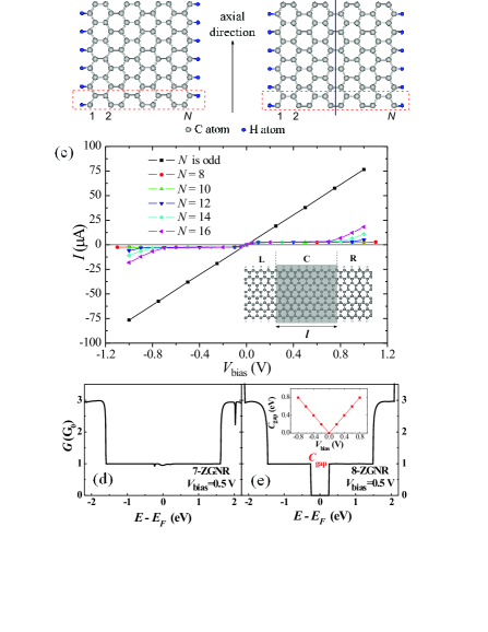
Thus far, in most studies of transport properties of GNRs, all GNRs with zigzag edges (ZGNRs) are treated as the same type, because they have very similar metallic electronic properties and transmission spectra under zero bias voltage White-ballistic ; Waka ; Peres ; Rojas . In this work, however, we will demonstrate that they can be classified into two groups that have completely different current-bias-voltage (-) characteristics (but similar band structures) with respect to whether there exists mirror plane [Figs. 1(a) and 1(b)]. Asymmetric ZGNRs behave as conventional conductors with one conductance quantum under bias voltages, whereas symmetric ZGNRs display very small currents because of the appearance of the conductance gap depending on the bias voltage. From a two-gates tight-binding (TB) model, this difference in transport properties is revealed to originate from different symmetries of ZGNRs, which is responsible for the different coupling properties between the subbands. Moreover, it is shown that the current through the symmetric ZGNRs can be remarkably enhanced by asymmetric edge terminations. This feature implies that the conduction of ZGNRs can be controlled by changing their symmetries via external modulations such as transverse electric fields.
We performed quantum transport calculations of ZGNRs by using an ab initio code, transiesta-c Taylor , which is based on real-space, nonequilibrium Green’s function formalism and the density-functional theory, as implemented in the siesta approach Soler . Self-consistent calculations are performed with a mixing rate of 0.05, and the mesh cutoff of carbon atom is chosen as 100 Ry. Our electronic structure calculations were performed using the ab initio siesta method Soler , which is based on the DFT within the local density approximation. In the calculations, structural optimizations were first carried out until atomic forces converged to 0.02 eV/. Except where specified, the edges of ZGNRs are terminated with hydrogen (H) atoms to remove the dangling bonds. Our calculations confirmed that the energy of the spin-polarized state (zero-temperature ground state) is 20 meV per edge atom lower than that of the spin-unpolarized state Louie-N ; Lee . However, the spin-polarized state would become unstable with respect to the spin-unpolarized state at finite temperature Wagner-66 or in the presence of a ballistic current through the GNRs White-circuit . In order to simulate the experimentally detectable transport behavior under bias voltages, we focused our study only on the spin-unpolarized metallic state of ZGNRs. To reveal the physical mechanism behind the results of ab initio calculations, we also employed the TB Green function method Rojas ; Datta ; wuapl to analyze the transmission spectra with a two-gates model.

As shown in Figs. 1(a) and 1(b), -ZGNRs notation can be divided into two groups with respect to their symmetries: i.e., odd(even) corresponds to asymmetric(symmetric) ZGNRs. In order to investigate the transport behaviors of ZGNRs under bias voltages, we carry out extensive first-principle calculations of - curves by using a two-probe system [shown in the inset of Fig. 1(c)], where left () and right () leads are semi-infinite ZGNRs. Figure 1(c) shows typical results for ZGNRs with different widths when the length of the central region () is of 8 unit cells. It is interesting to find that symmetric and asymmetric ZGNRs exhibit completely different transport characteristics, although they have very similar metallic band structures. In detail, all asymmetric ZGNRs (namely, is an odd number) have linear - curves with the same slope regardless of the ribbon width and length . As shown in Fig. 1(d), this result arises from the presence of one conductance quantum () around the Fermi level. On the other hand, all symmetric ZGNRs (namely, is an even number) have very small currents when is smaller than a critical bias-voltage (), beyond which the currents begin to increase. The conductance shown in Fig. 1(e) illustrates that this interesting phenomenon results from the presence of conductance gap () around the Fermi level under a certain . Furthermore, this conductance gap increases with increasing but is slightly smaller than [see the inset in Fig. 1(e)], and thus the current remains small until reaches .
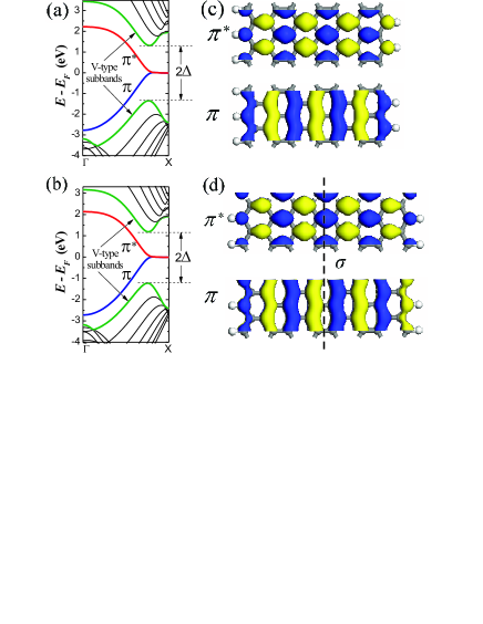
In general, distinct transport behaviors of two classes of ZGNRs arise from the characteristics of their electronic structure. However, as shown in Figs. 2(a) and 2(b), asymmetric and symmetric ZGNRs exhibit very similar band structures, which agree well with previous studies Louie-N ; Fujita99 . Around the Fermi level, there exist two partially flat bands (i.e., edge states) Fujita96 ; Nakada ; Fujita99 . As wavevector deviates from point, these two edge states mix to form bonding and antibonding states (i.e., and subbands) Waka-L ; Fazzio-Boron . In addition, there exist another two -type subbands around the Fermi level [see Figs. 2(a) and 2(b)]. Our calculations show that the energy gap between two -type subbands, , is inversely proportional to the width of ZGNR, consistent with previous TB studies Waka ; Beenakker-NP .

Clearly, different transport characteristics should come from something beyond the band structures. We turn to the wave functions of the and subbands, which are the only bands near the Fermi level and thus are responsible for the electron transmission under low bias voltages. As shown in Figs. 2(c) and 2(d), the wave functions of symmetric and asymmetric ZGNRs do exhibit different characteristics. In accordance with their symmetric geometry, the () subbands of symmetric ZGNRs have odd (even) parities under mirror operation. While the subbands of asymmetric ZGNRs have no definite parity, due to the absence of the mirror plane . Then, the problem becomes why the subband parity affects the electron transmission under bias voltage.

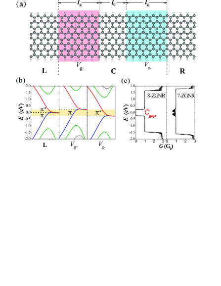
As is well known, one important effect of the bias voltage is that the chemical potential will change along the transport direction. To understand the influence of such change and subband parity on the transport behaviors, we design an ideal two-gates model [as shown in Fig. 3(a)] and calculate transmission spectra using the TB Green function method Rojas ; Datta ; wuapl . In the system, local gate voltages and are applied to the two gate regions separated by a buffer region, to simulate the change of chemical potentials [as shown in Fig. 3(b)]. Figure 3c shows the calculated transmission spectra of such a two-gate model for 8-ZGNR and 7-ZGNR with ==0.25 V. Evidently, they display a symmetry-dependent difference, which is the same as that of ZGNRs under a bias obtained by the ab initio transport simulation [Figs. 1(d) and 1(e)]. Then, a clear physical picture can be drawn from this result. As illustrated in Fig. 3(b), the local gates shift the Fermi level in the gate regions, and open an energy window (the yellow region), within which only subband exists in the region while only subband exists in the region. For symmetric ZGNRs, the and subbands have opposite parity, so they can not couple with each other to contribute to the transmission, and then a conductance gap appears [the left-hand panel of Fig. 3(c)]. For asymmetric ZGNRs, however, without the limitation of parity, a electron in the region may hop to a state in the region and contributes to the transmission, leading to the conductance of about 1 [the right-hand panel of Fig. 3(c)].
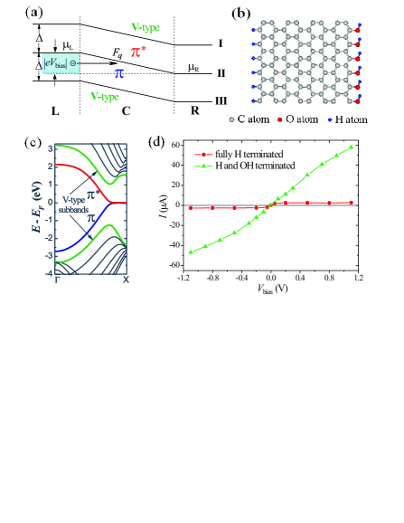
Then, the - curves of ZGNRs [shown in Fig. 1(c)] can be understood with the help of the schematic band diagram under [Fig. 4(a)]. Here, the solid line II represents the quasi-Fermi level () of the system. Lines I and III represent the critical energies at which -type subbands appear. So only () subband exists in the energy range between lines II and III (I). This feature of band structure is important for the unique transport behaviors of GNRs, and is different from that of armchair carbon nanotubes where both and subbands (crossing at the Fermi level) span the whole energy range. The bias voltage makes the chemical potentials of left and right leads ( and ) be separated by , and then only the electrons in the states between and [shaded blue area in Fig. 4(a)] can contribute to the current Datta . When , all these incident electrons into the central region are in the state, so the transmission through the system depends on whether electrons can hop to state or not. For symmetric ZGNRs, the hopping integral is zero due to parity limitation, and consequently the electrons will not flow through the ribbon and the current is very small. For asymmetric ZGNRs, however, there always exists conductance near the Fermi level [Fig. 1(d)] due to non-zero hopping integral between and electrons. On the other hand, when , -type subbands start to contribute to the conductance, and thus the currents through symmetric ZGNRs begin to increase.

Since the significant deviation from linear - dependence in symmetric ZGNRs (i.e., very small currents under a finite bias) originates from the symmetry of the system, it can be expected that breaking the symmetry may enhance the currents. To confirm this expectation, for original symmetric 8-ZGNR, we use hydroxyl group (OH) to terminate one edge while using H to terminate the other edge, and calculate its optimized structure, energy bands, and - curve as shown in Figs. 4(b)-4(d). Compared with the results of fully H-terminated 8-ZGNR [Fig. 2(b)], the energy bands do not change visibly, but the current under bias voltages increases remarkably. This happens because the asymmetric edge termination breaks the original mirror symmetry, and consequently and subbands no longer have definite parities. When a bias voltage is applied, and states can couple with each other and contribute to the conductance around the Fermi level, which leads to a notably increasing current. This also implies that the current through ZGNRs could be tuned by applying a transverse electric field along the direction perpendicular to the ribbon axes
In conclusion, symmetric and asymmetric ZGNRs are found to have completely different - characteristics despite the similarity of their band structure. Asymmetric ZGNRs behave as conventional conductors with one conductance quantum under bias voltages, whereas symmetric ZGNRs show very small currents because of the presence of conductance gap around the Fermi level. It is the different symmetry of ZGNRs that leads to different coupling between and subbands and consequently results in distinct transport behaviors. For symmetric ZGNRs, we further show that breaking the symmetry of electronic structure can effectively increase the current through ZGNRs. This might be useful in the design of electronic devices based on ZGNRs.
This work was supported by the National Natural Science Foundation of China (Grant Nos. 10325415, 10674077 and 10674078) and the Ministry of Science and Technology of China (Grant Nos. 2006CB605105 and 2006CB0L0601). The authors thank Qimin Yan and Zhirong Liu for helpful discussions.
References
- (1) K. S. Novoselov et al., Science. 306, 666 (2004).
- (2) C. Berger et al., J. Phys. Chem. B 108, 19912 (2004).
- (3) K. S. Novoselov et al., Nature (London) 438, 197 (2005).
- (4) Y. Zhang et al., Nature (London) 438, 201 (2005).
- (5) A. K. Geim, and K. S. Novoselov, Nat. Mater. 6, 183 (2007); M. I. Katsnelson, Mater. Today 10, 20 (2007).
- (6) C. Berger et al., Science 312, 1191 (2006).
- (7) M. Y. Han et al., Phys. Rev. Lett. 98, 206805 (2007).
- (8) Y.-W. Son, M. L. Cohen, and S. G. Louie, Phys. Rev. Lett. 97, 216803 (2006); V. Barone, O. Hod, and G. E. Scuseria, Nano Lett. 6, 2748 (2006).
- (9) D. Gunlycke, H. M. Lawler, and C. T. White, Phys. Rev. B 75, 085418 (2007); D. A. Areshkin, D. Gunlycke, and C. T. White, Nano Lett. 7, 204 (2007).
- (10) Q. M. Yan et al., Nano Lett. 7, 1469 (2007).
- (11) D. A. Areshkin, and C. T. White, Nano Lett. 7, 3253 (2007); D. Gunlycke et al., Nano Lett. 7, 3608 (2007).
- (12) K. Wakabayashi, Phys. Rev. B 64, 125428 (2001); K. Wakabayashi, and T. Aoki, Inter. J. Mod. Phys. B 16, 4897 (2002).
- (13) N. M. R. Peres, A. H. C. Neto, and F. Guinea, Phys. Rev. B 73, 195411 (2006).
- (14) F. Muñoz-Rojas et al., Phys. Rev. B 74, 195417 (2006).
- (15) K. Wakabayashi, and M. Sigrist, Phys. Rev. Lett. 84, 3390 (2000).
- (16) Y.-W. Son, M. L. Cohen, and S. G. Louie, Nature (London) 444, 347 (2006).
- (17) A. Rycerz, J. Tworzydło, and C. W. J. Beenakker, Nature Phys. 3, 172 (2007).
- (18) S. Datta, Electronic Transport in Mesoscopic Systems (Cambridge University Press, Cambridge, England, 1995).
- (19) J. Taylor, H. Guo, and J. Wang, Phys. Rev. B 63, 245407 (2001); M. Brandbyge et al., Phys. Rev. B 65, 165401 (2002).
- (20) J. M. Soler et al., J. Phys.: Condens. Matter 14, 2745 (2002).
- (21) H. Lee et al., Phys. Rev. B 72, 174431 (2005).
- (22) N. D. Mermin, and H. Wagner, Phys. Rev. Lett. 17, 1133 (1966).
- (23) J. Wu et al., Appl. Phys. Lett. 77, 2554 (2000).
- (24) Herein, is the number of zigzag chains across the ribbon width, and hence represents the width of ZGNR [as shown in Figs. 1(a) and 1(b)]. Also see Refs. [25-27] for details of this notation of GNR.
- (25) Y. Miyamoto, K. Nakada, and M. Fujita, Phys. Rev. B 59, 9858 (1999).
- (26) M. Fujita et al., J Phys. Soc. Jpn. 65, 1920 (1996).
- (27) K. Nakada et al., Phys. Rev. B 54, 17954 (1996).
- (28) T. B. Martins et al., Phys. Rev. Lett. 98, 196803 (2007).