Single electron tunneling through high- single-wall carbon nanotube NEMS resonators
Abstract
![[Uncaptioned image]](/html/1004.5362/assets/x1.png)
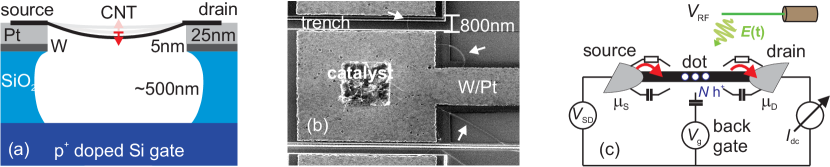
(a) Sketch of the basic experimental setup, with a nanotube
nano-electromechanical resonator being driven contact-free via the electric field of a
suspended radio-frequency antenna. (b) Gate voltage dependence of the observed mechanical
resonance frequency for the fundamental bending mode of the nanotube resonator as well as
higher modes.
By first lithographically fabricating contact electrodes and then as last step growing carbon nanotubes with chemical vapour deposition across the ready-made chip, many potential contamination mechanisms for nanotube devices can be avoided. Combining this with pre-defined trenches on the chip, such that the nanotubes are freely suspended above the substrate, enables the formation of highly regular electronic systems.
We show that, in addition, such suspended ultra-clean nanotubes provide excellent high-frequency and low-dissipation mechanical resonators. The motion detection mechanism of our experiment is discussed, and we measure the effect of Coulomb blockade and the back-action of single electron tunneling on the mechanical motion. In addition data on the mechanical higher modes is presented.
I Introduction
The mechanical properties of carbon nanotubes have by now inspired research for quite some time Treacy et al. (1996); Lu (1997); Yu et al. (2000). While applications mainly focus on bulk tensile strength, the low mass combined with the record Young’s modulus also leads to extremely high resonance frequencies of doubly clamped single-wall carbon nanotube resonators Sazonova et al. (2004); Witkamp et al. (2006). In the respective nano-electromechanical devices, a single suspended carbon nanotube is clamped between metallic leads, similar to a guitar or violin string. Motion is detected via the electrical conductance of the sample.
As a single-wall carbon nanotube is a clean, defect-free and chemically relatively inert macromolecule, it should act as a near-ideal mechanical beam resonator. However, for a long time the observed mechanical quality factors were quite low. All published experiments used basically identical fabrication techniques – lithographically defining contacts on top of a carbon nanotube, followed by wet-chemical underetching – and the same frequency downmixing detection of mechanical motion (for details see e.g. Sazonova et al. (2004); Witkamp et al. (2006)). At room temperature, typical results were Sazonova et al. (2004); Witkamp et al. (2006); Jensen et al. (2008), which was increased to in low-temperature measurements Lassagne et al. (2008); Poot et al. (2010).
Whereas the detailed mechanism limiting the observable in these measurements is still a matter of debate, two practical points immediately come into mind: a) the fabrication process where wet chemical treatment, resist residues, and electron beam irradiation can lead to deterioration of the mechanical properties, and b) the measurement process where two high-frequency signals are directly coupled into the high-impedance nanostructure, leading to noise contributions and heating of the resonator.
In the following sections we will address these two issues and show how optimization of both fabrication and measurement leads to much higher mechanical resonator quality factors and thereby frequency resolution in clean electronic systems Hüttel et al. (2009); Steele et al. (2009a), making a rich spectrum of interesting physics observable.
II Device fabrication
Figure 1(a) displays a simplified sketch of the chip geometry used in our experiments; a scanning electron microscope picture of a device from the same fabrication process as the measured one is shown in Fig. 1(b). The full details of the device layout and the fabrication process can be found in Steele et al. (2009b). The important modification of the fabrication process compared to previous measurements is that all lithographic processes for definition of on-chip structures are completed before carbon nanotube growth. This includes the definition of tungsten/platinum electrodes as well as the etching of the surface layers to generate a trench over which the carbon nanotubes will be suspended. After localized growth catalyst deposition, the devices are then finshed in a chemical vapour deposition step, see Kong et al. (1998). In this step, nanotubes grow across the electrodes and the pre-defined trench between them, which on this particular sample spans . Since with this technique, as pioneered in Cao et al. (2005), no lithography or wet chemistry takes place after nanotube growth, the macromolecules remain chemically and physically undamaged and free from resist residues or other contamination.
In addition to providing better mechanical properties, the electronic properties of the nanotube structures improve as well. This directly follows from the absence of fabrication-induced defects and charges trapped at surface contaminations. While Ref. Hüttel et al. (2009) is the first observation of the mechanical properties of such devices, several recent studies have already used them for fundamental research on trapped electronic systems Cao et al. (2005); Deshpande and Bockrath (2008); Kuemmeth et al. (2008).
III Dc current detection of mechanical resonance
III.1 Measurement setup
After completion of the fabrication steps, the device was placed in a dilution refrigerator, contacted electrically via low-pass filtered dc cabling only. The measurement is described schematically by the sketch of Fig. 1(c). At the dilution refrigerator base temperature of , the electronic system within the suspended carbon nanotube acts as a highly regular quantum dot, with the four-fold orbital level degeneracy typical for a clean single-wall carbon nanotube Oreg et al. (2000).
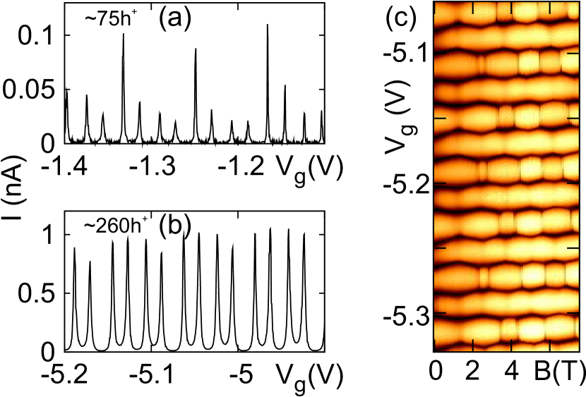
This is demonstrated in Fig. 2(a,b), displaying in the linear conductance regime. The device can be tuned from very weak (a) to strong coupling (b) between the quantum dot and its contacts by application of a back gate voltage alone, making both strong Coulomb blockade and the Kondo regime Goldhaber-Gordon et al. (1998a, b) accessible. As shown in Fig. 2(c), the regularity of the transport spectrum extends to level spectroscopy in a magnetic field, where multiple indications of orbital and singlet-triplet Kondo effects at ground state transitions, i.e. level degeneracy, can be observed Jarillo-Herrero et al. (2005a, b).
As already mentioned, previously the mechanical resonance of suspended nanotubes has been detected by means of the so-called frequency downmixing technique Sazonova et al. (2004); Witkamp et al. (2006); Lassagne et al. (2008); Poot et al. (2010). This requires the application of two high frequency signals directly to the nanotube device. The minimal temperature is thus limited by the thermal coupling of the high frequency leads to the cold finger of the cryostat, as well as by heating effects induced by the direct introduction of high-frequency signals. Nevertheless, an improvement of the quality factor up to at millikelvin temperatures has been observed Poot et al. (2010). In contrast, in the measurements described here, only one high-frequency driving signal is applied contact-free – i.e., as radiation from an antenna. The antenna, consisting of the open end of a coaxial cable with its shield removed, is suspended freely in the inner vacuum chamber of the dilution refrigerator at a distance of approximately from the sample surface.
III.2 Observation of the mechanical bending mode
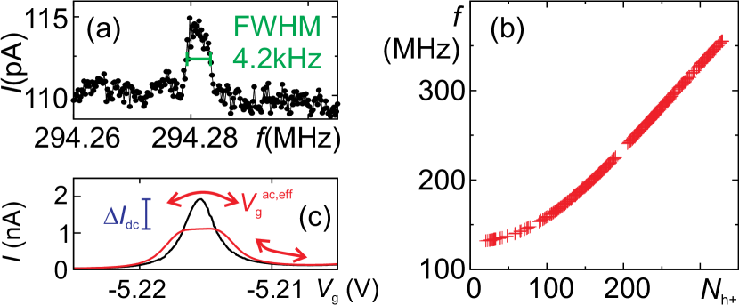
When measuring the dc single electron tunneling current through the carbon nanotube quantum dot while sweeping the frequency of the applied driving signal, a resonant feature emerges even at low driving power. Figure 3(a) displays a typical example for this frequency response at , and a nominal driving power of . The sharpness of the response in frequency, with a full width at half maximum in this case here of and values observed as small as at center frequency , indicates a high quality factor of the underlying resonator system. Fig. 3(b) plots the gate voltage dependence of this resonance frequency over the entire measured range of , scaled as function of the number of holes charged on the nanotube quantum dot . The observed shift indicates that indeed a mechanical resonance is observed, since in this case the resonance frequency is tuned by the electrostatically induced tension Sazonova et al. (2004). A comparison with a model for the bending mode of a bulk beam resonator Witkamp et al. (2006); Poot et al. (2007); Hüttel et al. (2009) confirms the mechanical origin of the current peak (see Hüttel et al. (2009)). At low gate voltage the model agrees with the data very well for and , where is the resonance frequency in absence of tension and marks the crossover between weak and strong bending regime Hüttel et al. (2009). At high negative gate voltages , model and measurement diverge in the region of high mechanical tension. The origin of this is still to be determined, however it may be related to more complex (i.e. partly longitudinal) motion of the nanotube resonator or to limitations of the model approximations for the bending rigidity.
III.3 Motion detection mechanism
While the phenomenological behaviour of the observed resonance clearly indicates the nanotube bending vibration mode as its origin, it has not been adressed so far how the mechanical resonance actually becomes visible in dc current. Fig. 3(c) illustrates a straightforward mechanism. The black line depicts a measured Coulomb blockade oscillation of current in absence of any radio-frequency signal. Conventionally in such a plot the gate voltage is chosen as x-axis parameter, however the parameter actually entering the equations is the product of the voltage and the gate capacitance, .
At resonant driving of the nanotube, the amplitude of the driving-induced oscillatory motion of the nanotube resonantor is strongly enhanced. This motion of the quantum dot with respect to the chip substrate modifies , and thereby also the potential on the dot induced by the back gate electrode. Thereby, the mechanical motion of the nanotube acts equivalently to an ac gate voltage superimposed on the statically applied dc gate voltage .
The mechanical resonance frequencies in the MHz range are far above the bandwidth of the dc amplifiers used at the current detection side. The measurement thus averages over the oscillation period, and thereby over the potential dependence of the source-drain current. Since this dependence is – due to the Coulomb blockade oscillations – strongly nonlinear, the peak shapes are smeared out. This is indicated by the red line in Fig. 3(c), obtained by numerical averaging from the measured data. The averaging at mechanical resonance this way leads to an effective dc current contribution , indicated in the plot for the case of the current maximum. Recently, a very similar mechanism has also been observed in a suspended resonator containing an aluminum single-electron transistor Pashkin et al. (2010).
Assuming an arbitrary non-linear function and a harmonic oscillation of the mechanical system with deflection , we obtain for the current time-averaged over the oscillation period
| (1) |
The change in current due to the mechanical motion with amplitude can be estimated by approximating the function as a Taylor series up to second order in , and by linearizing the geometrical capacitance around the equilibrium position of the nanotube . We then obtain as function of the motion amplitude
| (2) |
Note that we are assuming here and in later argumentation that the single electron tunneling current is a well-defined function of the nanotube position at each point in time of its motion . This means that electronic tunneling into and out of the nanotube quantum dot takes place at timescales much faster than the mechanical oscillation. The assumption agrees well with our experiment; for weaker and weaker coupling between quantum dot and leads the mechanical signal loses amplitude and at some point vanishes. At the last Coulomb blockade oscillations where it can still be observed (), the current in large-bias single electron tunneling () reaches values of . This current corrsponds to a lower bound for the tunnel frequency of , compared to a mechanical resonance frequency in this gate region of .
III.4 Mechanical quality factor
The quality factor of a resonator is defined as the ratio between the resonator’s center frequency and its bandwidth, i.e. the full width half maximum of the stored energy of the steady state oscillations as function of frequency . In the case of a mechanical harmonic oscillator, the energy scales with the square of the oscillation amplitude; using eq. 2 we obtain
| (3) |
This way, the resonator quality factor equals the ratio of center frequency and full width half maximum of the measured current peak, enabling straightforward determination. As already mentioned, values of up to have been observed; for the details we would like to refer to Hüttel et al. (2009).
IV Mechanical motion and single electron tunneling
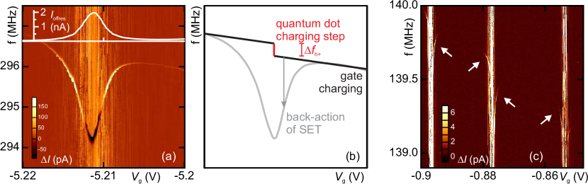
So far, the detailed nature of Coulomb blockade and single electron tunneling has not been taken into account; for the motion detection mechanism any nonlinear gate voltage dependence of the measured dc current is sufficient. In addition, the plot of Fig. 3(c) displays the gate voltage dependence of the observed mechanical resonance frequency only with a limited resolution. Zooming in, Fig. 4(a) shows the mechanical resonance signal across a single Coulomb blockade oscillation, providing a resolution in gate voltage higher by a factor 250 than Fig. 3(c). The plotted signal is the dc current as function of gate voltage and driving frequency . For each data column () the average current value has been subtracted to increase the contrast of the sharp resonance peak in . The bias voltage is set to , such that the quantum dot passes through regions of both single electron tunneling and Coulomb blockade. This is illustrated by the white line plot insert, which displays the dc current measured for off-resonant driving frequency, using the same x-axis as the main plot.
Across the single electron tunneling region a clear minimum of the mechanical resonance frequency can be observed. In Coulomb blockade, approaches a linear dependence on gate voltage, however the tangential lines are shifted for different charge on the quantum dot. Fig. 4(b) sketches the detailed behaviour as it repeats itself for each Coulomb blockade oscillation over a large range of the quantum dot charge. As we will see, different details of Figs. 4(a,b) correspond to different aspects of the coupled electromechanical system.
IV.1 Integer charge on nanotube
In room temperature measurements a smooth and monotonous dependence of the mechanical resonance frequency on the gate voltage is both expected and observed Sazonova et al. (2004); Witkamp et al. (2006). In contrast, at low temperatures and in the Coulomb blockade regime the charge located on the nanotube is discrete, and can only change by integer multiples of the elementary charge. In Sapmaz et al. (2003) it was already predicted that this should lead to a steplike behaviour of the mechanical resonance frequency. The step size , as indicated in the sketch of Fig. 4(b), corresponds to the increase in tension due to addition of a single elementary charge on the nanotube, whereas the finite slope between the steps is caused by the continuously varying charge on the back gate electrode.
In a simple picture the electrostatic force on the nanotube per additional elementary charge should grow linearly with the electric field between nanotube and gate and thereby the charge on the back gate electrode. Indeed, a clear gate voltage dependence of the frequency step size has been observed, with values varying from at () to at (). A detailed analysis of the functional dependence would however require additional data.
IV.2 Back-action on the mechanical motion
Overlaid on the skewed step function are clear minima of the resonance frequency whenever single electron tunneling takes place. In addition to static and radio frequency driving force, now the fluctuation of the electric charge contributes to the motion. As presented in more detail in Steele et al. (2009a), this dynamical effect adds an effective softening spring constant. This leads to dips in the resonant frequency up to an order of magnitude greater than the shifts induced by one more elementary charge on the nanotube. The resulting “Coulomb blockade oscillations of mechanical resonance frequency” are illustrated in the measurement of Fig. 4(c). Here the mechanical resonance can be traced across three Coulomb blockade oscillations, with the characteristic repetition of the pattern of Figs. 4(a,b).
To describe the underlying mechanism we need to point out that at finite temperature and finite dot–leads coupling the charge carrier number on the quantum dot fluctuates by one over a finite potential region. Across this region, the time-averaged charge varies smoothly with the potential. Now we again assume that electronic tunneling takes place at a much faster timescale than mechanical motion. This means that is well-defined for each point of the mechanical oscillation cycle. Motion of the of the resonator towards the gate leads to an increase of the gate capacitance , which influences a larger charge on the resonator, in turn increasing the force which pulls it towards the gate. The fact that the electrostatic force on the nanotube depends on the displacement means that an effective modification of the spring constant takes place.
Quantitatively, the nano-electromechanic spring constant contribution is proportional to . As detailed in Steele et al. (2009a), at low bias the charge on the quantum dot changes over a small gate voltage region, leading to a narrow and deep dip in the resonance frequency . In contrast, at high bias the charge can change gradually over the single electron tunneling region, resulting in a broad and shallow response of the mechanical resonance frequency.
V Higher mechanical resonator modes and outlook
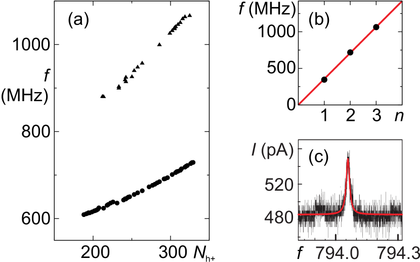
Already in the first measurements on nanotube beam resonators not only the fundamental flexural mode, but also other mechanical resonances were observed Sazonova et al. (2004). The simplicity of the radio-frequency part of our setup enables us to transfer this to significantly higher frequencies. This is illustrated in Fig. 5(a), where two higher mechanical modes are traced over a large range of nanotube charge and thereby mechanical tension. The obtained frequency values at (), i.e. in the high-tension limit, are plotted in Fig. 5(b) as function of the mode number . As expected for a string under high mechanical tension, the higher vibration mode frequencies () approach integer multiples of the fundamental vibration mode frequency (). This also confirms that we indeed observe the fundamental mode and the second and third flexural mode of the nanotube resonator.
Fig. 5(c) displays a corresponding current signal at low driving power, with a symmetric frequency response as expected for a harmonic oscillator. A mechanical response can be found at frequencies of , and even at higher frequencies signals may still be discovered through careful filtering of the raw measurement data.
The frequency scale of is significant insofar as it corresponds via to a temperature of , which can easily be obtained with state-of-the-art dilution refrigerators. This way, the transition between a “classical” nanotube beam resonator and a quantum mechanical harmonic oscillator comes into experimental reach Schwab and Roukes (2005); O’Connell et al. (2010). Higher resonator modes are however not the only method of approaching the quantum regime. The bending vibration mode frequency depends strongly on the length of the resonator, scaling with . Current nanofabrication techniques enable definition of structures significantly smaller than the resonator length of the device presented here. While the greater challenge for quantum-nano-electromechanical systems will likely lie in the development of driving-free sensitive motion detection schemes, nanotube resonators provide a highly attractive material system and may well be at the core of many interesting future experiments.
Acknowledgments. This research was carried out with financial support from the Dutch Foundation for Fundamental Research on Matter (FOM), The Netherlands Organisation for Scientific Research (NWO), NanoNed, and the Japan Science and Technology Agency International Cooperative Research Project (JST-ICORP). A. K. H. acknowledges financial support by the Deutsche Forschungsgemeinschaft (DFG) via SFB 689/A1.
References
- Treacy et al. (1996) M. M. J. Treacy, T. W. Ebbesen, and J. M. Gibson, Nature 381, 678 (1996).
- Lu (1997) J. P. Lu, Phys. Rev. Lett. 79, 1297 (1997).
- Yu et al. (2000) M.-F. Yu, B. S. Files, S. Arepalli, and R. S. Ruoff, Phys. Rev. Lett. 84, 5552 (2000).
- Sazonova et al. (2004) V. Sazonova, Y. Yaish, H. Üstünel, D. Roundy, T. A. Arias, and P. L. McEuen, Nature 431, 284 (2004).
- Witkamp et al. (2006) B. Witkamp, M. Poot, and H. van der Zant, Nano Lett. 6, 2904 (2006).
- Jensen et al. (2008) K. Jensen, K. Kim, and A. Zettl, Nature Nanotech. 3, 533 (2008).
- Lassagne et al. (2008) B. Lassagne, D. Garcia-Sanchez, A. Aguasca, and A. Bachtold, Nano Lett. 8, 3735 (2008).
- Poot et al. (2010) M. Poot, B. Witkamp, and H. S. J. van der Zant, in preparation (2010).
- Hüttel et al. (2009) A. K. Hüttel, G. A. Steele, B. Witkamp, M. Poot, L. P. Kouwenhoven, and H. S. J. van der Zant, Nano Letters 9, 2547 (2009).
- Steele et al. (2009a) G. A. Steele, A. K. Hüttel, B. Witkamp, M. Poot, H. B. Meerwaldt, L. P. Kouwenhoven, and H. S. J. van der Zant, Science 325, 1103 (2009a).
- Steele et al. (2009b) G. A. Steele, G. Götz, and L. P. Kouwenhoven, Nature Nanotechnology 4, 363 (2009b).
- Kong et al. (1998) J. Kong, H. T. Soh, A. M. Cassell, C. F. Quate, and H. Dai, Nature 395, 878 (1998).
- Cao et al. (2005) J. Cao, Q. Wang, and H. Dai, Nature Materials 4, 745 (2005).
- Deshpande and Bockrath (2008) V. V. Deshpande and M. Bockrath, Nature Physics 4, 314 (2008).
- Kuemmeth et al. (2008) F. Kuemmeth, S. Ilani, D. C. Ralph, and P. L. McEuen, Nature 452, 448 (2008).
- Oreg et al. (2000) Y. Oreg, K. Byczuk, and B. I. Halperin, Phys. Rev. Lett. 85, 365 (2000).
- Jarillo-Herrero et al. (2005a) P. Jarillo-Herrero, J. Kong, H. S. J. van der Zant, C. Dekker, L. P. Kouwenhoven, and S. De Franceschi, Physical Review Letters 94 (2005a).
- Jarillo-Herrero et al. (2005b) P. Jarillo-Herrero, J. Kong, H. S. J. van der Zant, C. Dekker, L. P. Kouwenhoven, and S. De Franceschi, Nature 434, 484 (2005b).
- Goldhaber-Gordon et al. (1998a) D. Goldhaber-Gordon, H. Shtrikman, D. Mahalu, D. Abusch-Magder, U. Meirav, and M. A. Kastner, Nature 391, 156 (1998a).
- Goldhaber-Gordon et al. (1998b) D. Goldhaber-Gordon, J. Göres, M. A. Kastner, H. Shtrikman, D. Mahalu, and U. Meirav, Physical Review Letters 81, 5225 (1998b).
- Poot et al. (2007) M. Poot, B. Witkamp, M. A. Otte, and H. S. J. van der Zant, Physica Status Solidi (b) 244, 4252 (2007).
- Pashkin et al. (2010) Y. A. Pashkin, T. F. Li, J. P. Pekola, O. Astafiev, D. A. Knyazev, F. Hoehne, H. Im, Y. Nakamura, and J. S. Tsai (2010), arXiv:1004.3074.
- Sapmaz et al. (2003) S. Sapmaz, Y. Blanter, L. Gurevich, and H. S. J. van der Zant, Phys. Rev. B 67, 235414 (2003).
- Schwab and Roukes (2005) K. C. Schwab and M. L. Roukes, Physics Today 58, 36 (2005).
- O’Connell et al. (2010) A. D. O’Connell, M. Hofheinz, M. Ansmann, R. C. Bialczak, M. Lenander, E. Lucero, M. Neeley, D. Sank, H. Wang, M. Weides, et al., Nature 464, 697 (2010).