Titanium Nitride Films for Ultrasensitive Microresonator Detectors
Abstract
Titanium nitride (TiNx) films are ideal for use in superconducting microresonator detectors because: a) the critical temperature varies with composition ( K); b) the normal-state resistivity is large, , facilitating efficient photon absorption and providing a large kinetic inductance and detector responsivity; and c) TiN films are very hard and mechanically robust. Resonators using reactively sputtered TiN films show remarkably low loss () and have noise properties similar to resonators made using other materials, while the quasiparticle lifetimes are reasonably long, . TiN microresonators should therefore reach sensitivities well below .
pacs:
07.57.Kp,03.67.Lx,74.25.nn,85.25.Oj,85.25.PbAbsorption of photons with in a superconductor breaks Cooper pairs into electrons or ”quasiparticles”, producing a perturbation of the the complex conductivity.Bluzer (1995); Gulian and Van Vechten (1995); Sergeev and Reizer (1996) Such perturbations may be readily sensed through vector microwave measurements of lithographed microresonators, and frequency multiplexing enables large detector arrays.Mazin et al. (2002); Day et al. (2003) These devices are commonly known as microwave kinetic inductance detectors, or MKIDs because the inductive (frequency shift) signal is considerably larger (). However, the dissipation signal can be more sensitive,Gao et al. (2007) especially at lower modulation frequencies, because the resonator frequency exhibits noiseDay et al. (2003); Mazin (2004); Gao et al. (2007); Barends et al. (2009) caused by a surface distribution of two-level system (TLS) fluctuators.Gao et al. (2007); Kumar et al. (2008); Gao et al. (2008); Gao (2008); Noroozian et al. (2009) In this letter, we discuss the requirements for ultrasensitive MKIDs and show that they are very well fulfilled by the measured properties of titanium nitride (TiN) films.
For dissipation readout using the standard shunt-coupled, forward transmission () configurationDay et al. (2003), the amplifier contribution to the noise equivalent power (NEP) is given by
| (1) |
Here is the number of quasiparticles in the detector active volume ; is the efficiency with which photon energy is converted to quasiparticles;Day et al. (2003) is the quasiparticle lifetime; is the amplifier noise temperature; is the microwave readout power absorbed by the quasiparticles; is optimized by matching the coupling and internal quality factors to give a resonator quality factor ; and is the fraction of the resonator’s internal dissipation that is due to resistive quasiparticle losses (). In terms of the microwave generator power incident on the feedline, For frequency readout, the amplifier NEP is reduced by a factor of ; however, TLS noise may then be an issue. Note that equation (1) does not include the transmission of the optical system or the absorption efficiency of the detector.
For minimizing the amplifier NEP, should be chosen so that the microwave and optical quasiparticle generation rates are about equal, provided that the optical loading is high enough that the quasiparticle dissipation dominates (). In this case, amplifier noise temperatures of order 1-10 K are sufficient to achieve the photon noise limit in the mm/submm/far-infrared bands.Gao (2008) In this letter we are primarily concerned with the lowest NEP values achievable, so we examine the opposite limit of vanishingly small optical power and a correspondingly small quasiparticle population. Other dissipation mechanisms (radiation, TLS, grain boundaries, etc.) will then limit the resonator quality factor to some maximum value , so . Also, the quasiparticle lifetime is observedBarends et al. (2008); Kozorezov et al. (2008); Barends et al. (2009) to reach a maximum value for densities . If thermally generated quasiparticles are made insignificant by cooling and other sources of stray power are eliminated,Martinis et al. (2009) readout power dissipation remains as the only source of quasiparticles, which are generated with some efficiency . Eqn. (1) then yields
| (2) |
Here is the kinetic inductance fraction,Day et al. (2003) is a dimensionless Mattis-Bardeen factor of order unity,Mattis and Bardeen (1958); Gao (2008) and is the single-spin density of states at the Fermi energy. Thus, is a useful figure of merit. In addition, the gap parameter plays a crucial role: because . We will show that for TiN is considerably better than for other materials explored to date.
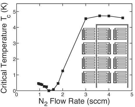
Although good resonators can be made with K NbTiN films,Barends et al. (2008, 2009) lower- materials are needed for sensitive detectors. We therefore studied TiNx films produced by reactive magnetron sputtering onto ambient-temperature, 100 mm diameter, high resistivity () HF-cleaned silicon substrates. The titanium sputtering target was 99.995% pure, and the sputtering gases (N2 and Ar) were 99.9995% pure. As shown in Fig. 1, the TiN film is sensitive to composition.Spengler et al. (1978) Microresonator structures were fabricated using deep UV projection lithography followed by inductively coupled plasma etching using a chlorine chemistry (BCl3/Cl2). Both distributed coplanar waveguide (CPW) resonatorsDay et al. (2003); Gao et al. (2007) as well as lumped-element resonatorsDoyle et al. (2008) with meandered inductors and interdigitated capacitors (see Fig. 2) were produced.
For our TiN films with and , the normal-state resistivity was typically , with . This resistivity is similar to polycrystalline TiN films reported in the literature but considerably higher than for single-crystal films.Johansson et al. (1985) The high resistivity (relative to Al, Ta, or Nb) is very convenient for obtaining highly efficient far-infrared photon absorption in lumped-element resonator structures.Doyle et al. (2008) As a consequence of the Mattis-Bardeen relationship between the normal-state surface resistance and the superconducting surface inductance , the large resistivity also guarantees a large kinetic inductance fraction .
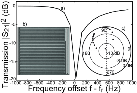
Fig. 2b shows a lumped-element 1.5 GHz TiN resonator consisting of a meandered inductor and an interdigitated capacitor (IDC), designed to serve as a pixel in a far-IR imaging array that is read out using a single coplanar strip (CPS) feedline. The array and feedline geometry is shown schematically in the inset to Fig. 1; the spacing between pixels is around 60 . The IDC consists of four 0.9 mm vertical strips with relatively large gaps to reduce noise and dissipationNoroozian et al. (2009), while the inductor consists of 32 1 mm horizontal strips and has and . Experiments using a cryogenic blackbody source and a metal-mesh, wavelength bandpass filter verify the basic functionality of these devices and show that the meander is an efficient single-polarization absorber.
Although the resonators were predicted to have , the measured values for the array show a very large scatter , which is largely due to unanticipated multi-resonator modes arising from pixel-pixel coupling. Indeed, electromagnetic simulations show that two isolated, identically tuned, nearest-neighbor pixels would produce symmetric and antisymmetric coupled modes with a frequency splitting of MHz, so the interpixel coupling is much larger than the MHz intended resonator frequency spacing. We have since developed improved pixel designs and filled arrays with dramatically reduced coupling; these results will be reported in a future publication. However, the very large accidental values have fortunately enabled a deep probe of the microwave loss of TiN. As shown in Figs. 2a and 2c, the measurements imply . The interpretation of of the coupled modes is secure since all resonances displayed the same frequency vs. temperature curve and follow the Mattis-Bardeen prediction. Furthermore, the improved uncoupled resonators also show . Regarding lower- material, to date our results indicate that for 0.85 K TiN; higher- resonators will be needed to push this limit. The best Al or Nb resonators to date have ; however, for such high one must generally use thick films (nm) for which .Gao (2008) Therefore, whereas . We will consider the remaining factors in below.
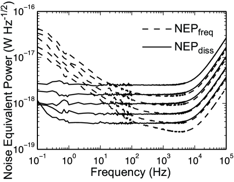
For ease of comparison to previous measurements, we studied the noise of a coplanar waveguide resonator with our standard geometry (see Fig. 3 for details). After correcting for the higher () characteristic impedance and third-harmonic operation for the TiN CPW deviceGao (2008), the measured frequency noise ( at dBm) may be compared to other resonators operated at internal power dBm, and is about a factor of two lower than typically seen.Gao et al. (2007) This result, along with the very similar spectral shape and power dependence, implies that the frequency noise of the TiN device almost certainly arises from surface TLS fluctuators. As with other materials, no dissipation fluctuations are seen above the cryogenic amplifier noise floor. The corresponding electrical NEP is at 1 Hz even though is quite modest. A smaller-volume resonator with should give an NEP in the few range.
For calculating NEP, it is necessary to assume a value for the electronic density of states . The results of Dridi et al.Dridi et al. (2002) are insensitive to stochiometry over our range of interestSpengler et al. (1978) and correspond to including the electron-phonon enhancement factor ,McMillan (1968); Isaev et al. (2007) or about a factor of two lower than for Al. However, recent workAllmaier et al. (2009) has indicated that electron correlation effects in TiN may reduce ; if so this would lower the NEP. Detection experiments with TiN resonators should help elucidate this issue.
Another important factor is the quasiparticle lifetime. From far-IR, UV, and X-ray photon detection experiments, we find lifetimes of for K material, for K, and for K, scaling roughly as as might be expected. For K, the lifetime is in the range seen for thin Al ( nm) films but is an order of magnitude shorter than the best thick ( nm) Al films.Barends et al. (2009)
Thus, the remaining factors contained in are about the same for TiN, thin Al, and thick Al, to within a factor of two. Therefore, the two orders of magnitude advantage in for TiN translates directly into a factor of 10 improvement in sensitivity, or for applications requiring large sensors, an improvement of two orders of magnitude in device area. Furthermore, the ability to reach high with TiN resonators should enable very dense MKID frequency multiplexing, and should also be of considerable interest for quantum information and other applications.
This research was carried out in part at the Jet Propulsion Laboratory (JPL), California Institute of Technology, under a contract with the National Aeronautics and Space Administration. The devices used in this work were fabricated at the JPL Microdevices Laboratory. This work was supported in part by the NASA Science Mission Directorate, JPL, and the Gordon and Betty Moore Foundation.
References
- Bluzer (1995) N. Bluzer, J. Appl. Phys., 78, 7340 (1995).
- Gulian and Van Vechten (1995) A. M. Gulian and D. Van Vechten, Appl. Phys. Lett., 67, 2560 (1995).
- Sergeev and Reizer (1996) A. V. Sergeev and M. Y. Reizer, Int. J. Mod. Phys. B, 10, 635 (1996).
- Mazin et al. (2002) B. A. Mazin, P. K. Day, J. Zmuidzinas, and H. G. LeDuc, AIP Conf. Proc., 605, 309 (2002).
- Day et al. (2003) P. Day, H. G. LeDuc, B. A. Mazin, A. Vayonakis, and J. Zmuidzinas, Nature, 425, 817 (2003).
- Gao et al. (2007) J. Gao, J. Zmuidzinas, B. A. Mazin, H. G. Leduc, and P. K. Day, Appl. Phys. Lett., 90, 102507 (2007).
- Mazin (2004) B. A. Mazin, Ph.D. thesis, California Institute of Technology, Pasadena CA (2004).
- Barends et al. (2009) R. Barends, H. L. Hortensius, T. Zijlstra, J. J. A. Baselmans, S. J. C. Yates, J. R. Gao, and T. M. Klapwijk, IEEE Trans. Appl. Supercond., 19, 936 (2009a).
- Kumar et al. (2008) S. Kumar, J. Gao, J. Zmuidzinas, B. A. Mazin, H. G. Leduc, and P. K. Day, Appl. Phys. Lett., 92, 123503 (2008).
- Gao et al. (2008) J. Gao, M. Daal, J. M. Martinis, A. Vayonakis, J. Zmuidzinas, B. Sadoulet, B. A. Mazin, P. K. Day, and H. G. Leduc, Appl. Phys. Lett., 92, 212504 (2008).
- Gao (2008) J. Gao, Ph.D. thesis, California Institute of Technology, Pasadena CA (2008).
- Noroozian et al. (2009) O. Noroozian, J. Gao, J. Zmuidzinas, H. G. Leduc, and B. A. Mazin, AIP Conf. Proc., 1185, 148 (2009).
- Barends et al. (2008) R. Barends, J. J. A. Baselmans, S. J. C. Yates, J. R. Gao, J. N. Hovenier, and T. M. Klapwijk, Phys. Rev. Lett., 100, 257002 (2008a).
- Kozorezov et al. (2008) A. G. Kozorezov, A. A. Golubov, J. K. Wigmore, D. Martin, P. Verhoeve, R. A. Hijmering, and I. Jerjen, Phys. Rev. B, 78, 174501 (2008).
- Barends et al. (2009) R. Barends, S. van Vliet, J. J. A. Baselmans, S. J. C. Yates, J. R. Gao, and T. M. Klapwijk, Phys. Rev. B, 79, 020509 (2009b).
- Martinis et al. (2009) J. M. Martinis, M. Ansmann, and J. Aumentado, Phys. Rev. Lett., 103, 097002 (2009).
- Mattis and Bardeen (1958) D. C. Mattis and J. Bardeen, Phys. Rev., 111, 412 (1958).
- Barends et al. (2008) R. Barends, H. L. Hortensius, T. Zijlstra, J. J. A. Baselmans, S. J. C. Yates, J. R. Gao, and T. M. Klapwijk, Appl. Phys. Lett., 92, 223502 (2008b).
- Spengler et al. (1978) W. Spengler, R. Kaiser, A. N. Christensen, and G. Müller-Vogt, Phys. Rev. B, 17, 1095 (1978).
- Doyle et al. (2008) S. Doyle, P. Mauskopf, J. Naylon, A. Porch, and C. Duncombe, J. Low Temp. Phys., 151, 530 (2008).
- Johansson et al. (1985) B. O. Johansson, J.-E. Sundgren, J. E. Greene, A. Rockett, and S. A. Barnett, J. Vac. Sci. Technol. A, 3, 303 (1985).
- Dridi et al. (2002) Z. Dridi, B. Bouhafs, P. Ruterana, and H. Aourag, J. Phys. Cond. Matt., 14, 10237 (2002).
- McMillan (1968) W. McMillan, Phys. Rev., 167, 331 (1968).
- Isaev et al. (2007) E. I. Isaev, S. I. Simak, I. A. Abrikosov, R. Ahuja, Y. K. Vekilov, M. I. Katsnelson, A. I. Lichtenstein, and B. Johansson, J. Appl. Phys., 101, 123519 (2007).
- Allmaier et al. (2009) H. Allmaier, L. Chioncel, and E. Arrigoni, Phys. Rev. B, 79, 235126 (2009).