Scattering of the near field of an electric dipole by a single-wall carbon nanotube
Abstract
The use of carbon nanotubes as optical probes for scanning near-field optical microscopy requires an understanding of their near-field response. As a first step in this direction, we investigated the lateral resolution of a carbon nanotube tip with respect to an ideal electric dipole representing an elementary detected object. A Fredholm integral equation of the first kind was formulated for the surface electric current density induced on a single-wall carbon nanotube (SWNT) by the electromagnetic field due to an arbitrarily oriented electric dipole located outside the SWNT. The response of the SWNT to the near field of a source electric dipole can be classified into two types, because surface-wave propagation occurs with (i) low damping at frequencies less than - THz and (ii) high damping at higher frequencies. The interaction between the source electric dipole and the SWNT depends critically on their relative location and relative orientation, and shows evidence of the geometrical resonances of the SWNT in the low-frequency regime. These resonances disappear when the relaxation time of the SWNT is sufficiently low. The far-field radiation intensity is much higher when the source electric dipole is placed near an edge of SWNT than at the centroid of the SWNT. The use of an SWNT tip in scattering-type scanning near-field optical microscopy can deliver a resolution less than nm. Moreover, our study shows that the relative orientation and distance between the SWNT and the nanoscale dipole source can be detected.
keywords:
carbon nanotube, current density, electric dipole, integral equation, near field, scattering, terahertz1 Introduction
Carbon nanotubes, hollow cylindrical rolls of graphene layers, possess remarkable electronic properties [1] as well as tremendous mechanical stability and strength [2] that makes them attractive for various applications in opto- and nano-electronics [3]. One of the focuses of current research is on the responses of carbon nanotubes to an externally applied electromagnetic field [4, 5, 6], because carbon nanotubes have prominent absorption resonances in the infrared and visible regimes, the resonance frequencies reflecting the carbon nanotube lattice symmetry [7]. Moreover, carbon nanotubes are strongly nonlinear optical structures [8, 4, 9] with an ultrafast optical response [10] that could be exploited for ultrafast optical signal-processing devices. Furthermore, as research advances, carbon nanotubes are no longer considered as infinitely long. The influence of the finite length through edge effects on the electromagnetic responses of carbon nanotubes is being investigated, particularly for carbon nanotubes operating as receiving nanoantennas. Reports have been published on isolated single-wall carbon nanotubes (SWNTs) [11, 12, 13], isolated multiwall carbon nanotubes [14], bundles of carbon nanotubes [15], and carbon nanotube arrays [16, 17]. Actual radio receivers utilizing an electromechanical modulation of the field emission from a carbon nanotube antenna have been successfully fabricated [18].
Most research in this context is devoted to the response of a carbon nanotube to a uniform plane wave. But a carbon nanotube’s response to the spatially nonuniform near field due to a closely located source ought to be substantially different from the planewave response of the same carbon nanotube, depending on the relating location and orientation of the carbon nanotube and the near-field’s source, as is known to be true for other scatterers [19, 20]. This can also be inferred from a theoretical analysis of the scattering of a plane wave jointly by a metallic nanosphere and an SWNT [21]. More recently, the intensity spectrum of the thermal radiation from an SWNT in the near-field zone was found to have additional resonant lines than its analog when the SWNT is in the far-field zone [22].
An understanding of the responses of carbon nanotubes in the near-field zone is crucial for scattering-type scanning near-field optical microscopy (sSNOM) and biomarking. A sharp tip placed in the proximity of the sample is used in sSNOM to scatter near fields induced on the sample surface by an external focused light beam. The scattered light involves near-field zone interaction between the tip and the sample and maps the surface characteristics of the sample in terms of a local refractive index and a local absorption coefficient [6]. Thus, a resolution on the order of several nm could be obtained by using an SWNT as a tip. Indeed, an resolution of 30 nm at 633-nm wavelength has already been reported [23]. In the rapidly developing field of the terahertz aperture-less near-field spectroscopy and microscopy [24], a resolution of 100 nm has been obtained with a tungsten tip [25, 26] and 30 nm with a platinum tip [27], and a proposal for SWNTs as tips has already been made [13].
Another possibility for using carbon nanotubes for SNOM would allow complementary spectroscopic characterization of the photoluminescence (PL) properties of nanoscale objects. A higher near-field intensity due to the tip changes and amplifies the signal from a source that is either a molecule or a man-made nano-object, with detection taking pave in the far-field zone [28]. Scanning along the surface produces the PL map with potentially subwavelength resolution being controlled by the apex radius of the probe.
Nanostructures that combine such multiple functionalities as biocompatibility, fluorescent signalling, and drug storage and delivery, will advance cancer diagnostics and therapeutics. Integration of carbon nanotubes with nanoscale luminescent materials such as quantum dots (QDs) appears promising [29]. This integration may be achieved by functionalizing carbon nanotubes with either DNA molecules [30] or carboxyl groups [29, 31] to which QDs could be attached. Integration of carbon nanotubes and QDs substantially affects the luminescence properties of QDs, corroborating the experimentally determined energy transfer between carbon nanotubes and QDs [31].
The foregoing examples amply demonstrate that the near-field responses of carbon nanotubes require a comprehensive investigation. As a first step in that direction, we examine the scattering of the near field of an oscillating, point electric dipole in the proximity of an SWNT of finite length—to address the effect of PL amplification and to understand the role of the SWNT antenna/near-field probe in the formation of the radiation pattern of a point PL source. The outline of the paper is as follows: The boundary-value problem is formulated in Sec. 2, and several typical profiles of the current induced on an SWNT are presented and discussed in Sec. 3. Our theory is intended to cover the coupling of a broad variety of luminescent nano-objects to an SWNT near-field probe. As the energy transfer between a nano-object and an SWNT can be either resonant or non-resonant, depending on the excitation frequency, illustrative examples are presented in Sec. 3. Section 3.3 is devoted to the special case of an endohedral molecule inside the SWNT, the molecule being modeled as a coparallel source electric dipole located on the SWNT axis. The resonant coupling of an SWNT placed close to a source electric dipole is examined in Sec. 4. Sec. 5 provides a detailed examination of the scattered electric field. Examining the contour plots of the far-zone field due to the dipole-SWNT system in Sec. 5.2, we determine the spatial resolution that an SWNT tip can deliver in sSNOM. Conclusions are provided in Sec. 6. Gaussian units are used, and a time dependence of is implicit with as time, as angular frequency, and . Vectors are denoted in boldface; unit vectors are denoted as , etc.; and dyadics [32] are double-underlined.
2 Boundary-value problem
Suppose an SWNT of length is exposed to the electromagnetic field radiated by a current density , where denotes the position vector. The electric field everywhere must satisfy the nonhomogeneous vector Helmholtz equation
| (1) |
where is the free-space wavenumber, is the speed of light in free space, and denotes the identity dyadic. Likewise, the magnetic field everywhere must be a solution of the related equation
| (2) |
If the cross-sectional radius of the SWNT is denoted by , the SWNT axis is aligned parallel to the axis of a Cartesian coordinate system , and the centroid of the SWNT is designated as the origin of the coordinate system, any point on the surface of the SWNT can be specified by
| (3) |
where are the Cartesian unit vectors. Using the equivalent cylindrical coordinate system , we have to enforce the satisfaction of the following boundary conditions [33, 34]
| (4) | |||
| (5) | |||
| (6) |
Here, , the surface current density induced on the SWNT’s surface , is a measure of the jump in the tangential magnetic field across that surface.
The surface electric current density is assumed to be independent of and purely axial: . For this statement to be valid, the electric field radiated by the current density needs to be homogeneous along the SWNT circumference. Thus the following restriction is imposed on the system under the consideration: . Based on the spatial variations of the electromagnetic field emitted by when the scattering SWNT is absent, additional restrictions may emerge too. Finally, it must satisfy the edge conditions
| (7) |
which express the absence of concentrated charges on the two edges of the SWNT.
Except in the source region, the electric field can be represented as [32, 35]
| (8) |
where the incident electric field
| (9) |
is due to the source current density that is confined to the region lying outside the SWNT, and the scattered electric field everywhere is given by
| (10) |
In these equations,
| (11) |
is the dyadic free-space Green function. Equations can be similarly written for the incident and the scattered magnetic fields, but are not needed.
An axial surface conductivity can be obtained to relate the jump in the tangential magnetic field across the surface of the SWNT to the axial electric field [33]; thus,
| (12) |
This equation is quite general, except that it does not take into account the effects of spatial dispersion as well as excitonic effects; furthemore, we have neglected the contribution of the chiral conductivity to the axial current because that contribution is quite small in SWNTs [36].
Taking the dot product of both sides of Eq. (10) with , and making use of Eqs. (8) and (12) therein, we obtain
| (13) |
where the scalar Hertz potential
| (14) |
According to our assumptions, changes so slowly along the SWNT circumference that it can be assumed to depend on the axial coordinate only; i.e., . Thereby, Eq. (13) becomes an integrodifferential equation for with the formal solution
| (15) |
where the constants have to be determined eventually using the edge conditions (7).
Equating the right sides of Eqs. (14) and (15), we obtain
| (16) |
with the kernel
| (17) |
Equation (16) is a Fredholm integral equation of the first kind with as the unknown function to be determined [37]. It has to be solved numerically for specified , as in a predecessor paper [13]. Once has been determined for all , the scattered electric field can be calculated at any location using Eqs. (7) and (10).
We chose the source of the near field to be a point electric dipole of moment located at outside the SWNT, as shown in Fig. 1; accordingly,
| (18) |
Substituting Eq. (18) on the right side of Eq. (9), we obtained
| (19) |
The electromagnetic field due to an electric dipole contains terms that vary as , , and , with the first term dominant in the near-field zone and the third term dominant in the far-field zone [32]. There are certain restrictions on and to ensure that the -directed component of the incident electric field varies very little along the circumference of the SWNT for any .
In the foregoing equations, we have implicitly assumed that the source incorporates interaction with the SWNT, and is therefore in a steady state in the presence of the SWNT. As such, it already includes possible renormalization of the dipole frequency (and lifetime). Such quantities can be computed knowing the ones in the absence of the SWNT, but that substantial exercise will be taken up in the future.
3 Typical Profiles of Induced Surface Current
Calculations were performed for two types of metallic and one type of semiconductor zigzag SWNTs—specified by the dual indexes , and , as is commonplace [4, 7]—each of length m. The axial surface conductivity was computed using the relaxation time s (except for those in Sec. 4) and the overlap integral eV, as shown elsewhere [33].
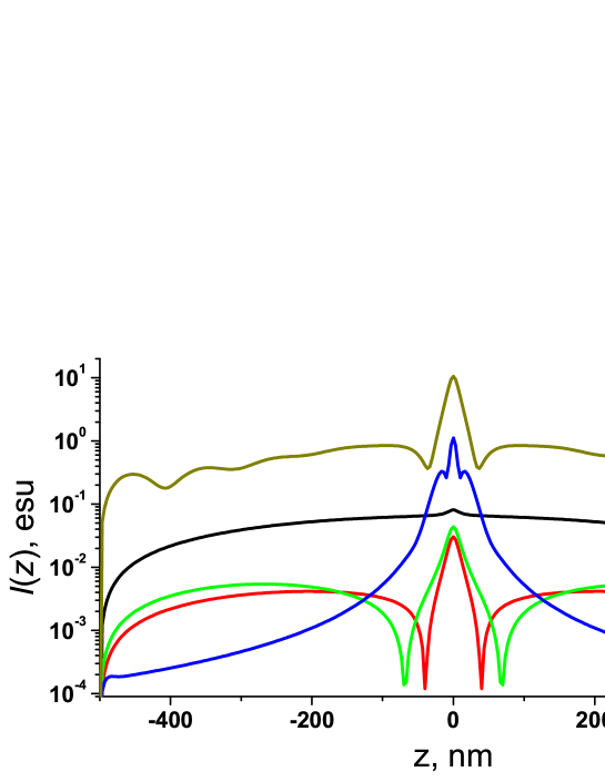
Two orientations of the electric dipole were considered: parallel to the SWNT axis and normal to the SWNT axis. The magnitude of the electric dipole moment was assumed equal to D esu, while the location was varied. We illustrate the frequency dependence of the electromagnetic coupling between the source and the SWNT in this section by computing profiles of the induced current at the following four different frequencies:
- (i)
-
(ii)
THz, an off-resonance frequency;
- (iii)
- (iv)
In addition, for the SWNT we chose
- (v)
The smallest free-space wavelength among these five cases is 229 nm. As the cross-sectional radius of the SWNT is nm and that of the SWNT is nm , both satisfy the condition .
3.1 Coupling to the near field of a source electric dipole
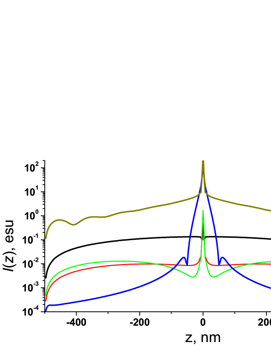
The calculated profiles of the electric current induced on the SWNT surface by the electric field (19) due to a source electric dipole are presented in
The remaining case— nm and esu—to complete a quartet turned out to be trivial for the following reason: When the electric dipole is situated on the SWNT axis and is directed normal to that axis, the -directed component of the incident electric field changes sign along any cross-sectional diameter of the SWNT. Thus, that component of the incident electric field cannot be assumed to be invariant across the circumference of the SWNT. However, as that component in one half of the SWNT bisected by the meridional plane to which the electric dipole is tangential is opposite in sign to that component in the other half, and consistently with the fully symmetric one-dimensional approximation allowed by the condition , we can assume that the coupling between the source electric dipole and the SWNT is negligibly small, at least to the first approximation.
In all other cases (Figs. 2 and 3) the source electric dipole is located 10 nm from the closest point on the SWNT, which distance is less than even at the largest frequency considered. Therefore, not surprisingly, the closest part of the SWNT is tightly coupled to the electric dipole and sustains a very large surface current density. Apart from that feature, which is common to all curves in Figs. 2 and 3, two different regimes of the SWNT’s response to the near field can be identified.
The first regime is the low-frequency (terahertz) regime for metallic SWNTs—represented by cases (i)–(iii)—wherein the SWNTs support surface-wave propagation with very low damping. In this regime the distribution of the surface current density is quite uniform along the length of the SWNT, subject, of course, to the edge conditions (7).
The second regime of the SWNT’s response to the near field is represented by cases (iv) and (v). These response characteristics are inherent
-
•
to metallic SWNTs in the high-frequency regime, where the contribution to from the interband electronic transitions becomes essential, and
-
•
to semiconducting SWNTs in the whole frequency range, as we show next.
Surface-wave propagation on the SWNT still occurs in the second regime, but with high damping [case (v)] and very high damping [case (iv)]. Accordingly, the surface-current-density profile is strongly peaked [case (v)] and very strongly peaked [case (iv)] closest to the electric dipole.
The surface current profile along the SWNT axis does not depend directly on the free-space wavelength , as the near field of dipole is strongly localized in the vicinity of the dipole. In order to confirm this issue, the current induced in the (14,0) SWNT by the electric dipole oscillating at the frequency 2.6 THz—which is the frequency of the first geometrical resonance in the (15,0) SWNT—is presented in Fig. 4. The dipole orientation and location are the same as for Fig. 2(a): esu and nm. The current distribution in the SWNT in Fig. 4 strongly resembles the current distribution in the SWNT at 500 THz—see Fig. 2(a)—though the wavelength is 200 times smaller in the second case. The only difference is the maximum value of the induced current that is much higher for the SWNT at 500 THz than for the SWNT at 2.6 THz.
The orientation of the electric dipole with respect to the SWNT axis has a significant effect on the profile of the induced current. Let us first look at Fig. 2, for the source electric dipole located in the central transverse plane of the SWNT. At any point on the SWNT axis, the incident electric field has only - and -directed components for . In the central part of the SWNT, the incident electric field is primarily axial (-directed) when the electric dipole is parallel, but primarily normal (-directed) when the electric dipole is normal, to the SWNT axis. Therefore, following Eq. (12), at the center of the SWNT the induced surface current is not null-valued in Fig. 2(a) but is null-valued in Fig. 2(b). Next, when the electric dipole is located on the SWNT axis, as for Fig. 3, the difference is even more prominent as a dipole oriented normal to the SWNT axis is not coupled to the SWNT at all.
3.2 Coupling to the far field of a source electric dipole
Thus far we have considered the SWNT located in the near-field zone of the source electric dipole. It is instructive to consider also the case when the SWNT is located in the far-field zone. Although this situation is not helpful to our goal of evaluating the possibility of SNOM applications, it gives additional insight on the interplay of the geometrical and frequency dependencies of the coupling between the source field and the electronic system of the SWNT.
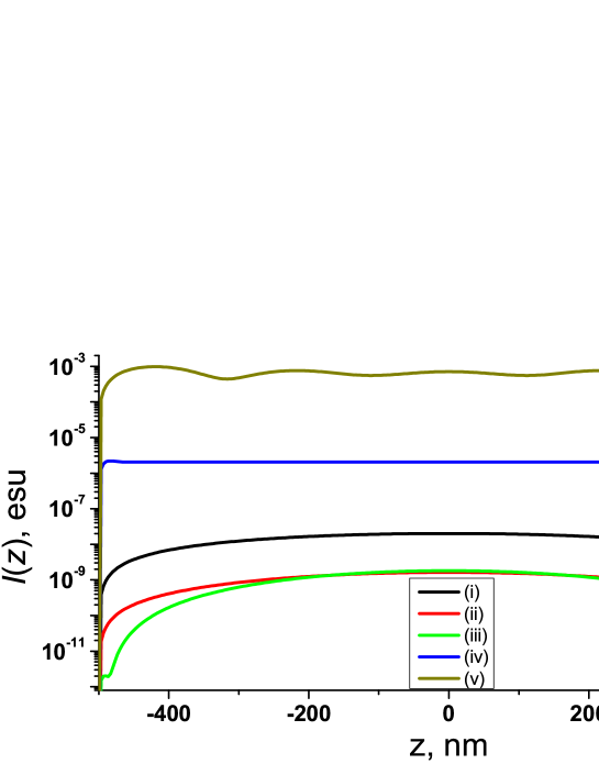
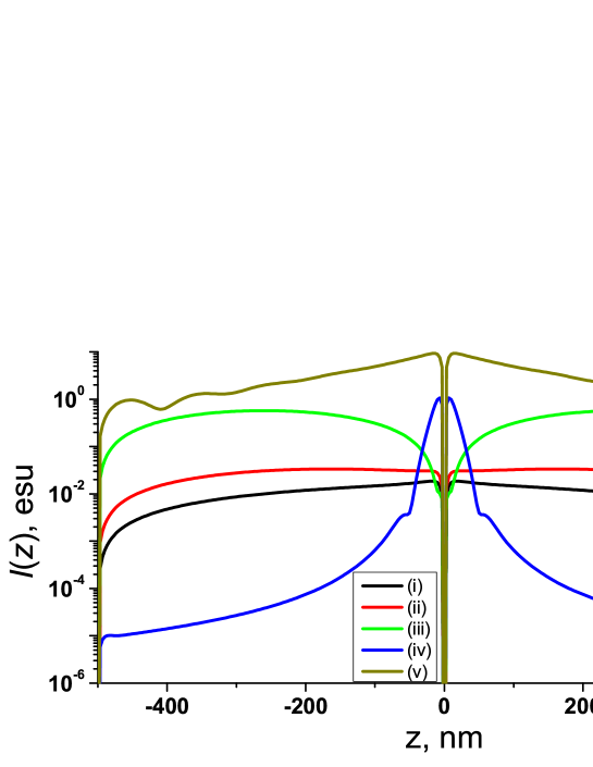
The profiles of the induced surface current computed for m and esu are presented in Fig. 5. Two response regimes are evident in this figure, just as in Fig. 2(a): one regime covers cases (i)–(iii), and the other spans cases (iv) and (v). The magnitude of the induced current is much smaller when m than when nm, because the incident electric field is much weaker in magnitude at any point on the SWNT when the SWNT is irradiated by the far field. The profile of the induced current tends to be more uniform for m than for nm, because every point on the SWNT lies in the far-field zone of the source electric dipole in the former scenario.
The oscillatory profile of the induced surface current in Fig. 5 for case (v) is due to the fact that the wavelength of the surface wave is nm. In order to explain this issue, let us recall that a surface wave with dependence on can travel on the SWNT, per [33, Eq. (57)]. The value of works out equal to cm-1, by virtue of [33, Eq. (58)], and the surface wave therefore has wavelength nm.
3.3 Coupling to a source electric dipole inside the SWNT
The formulation presented in Sec. 3 can be easily modified to to accommodate the location of the source electric dipole inside the SWNT, so long as the -directed component of the incident electric field depends on the axial coordinate only. This situation mimics the special case of an endohedral molecule inside the SWNT, the molecule being modeled as a coparallel source electric dipole located on the SWNT axis.
Accordingly, after setting , , and , we have to modify Eq. (15) to
| (20) | |||||
with the tacit understanding that is independent of .
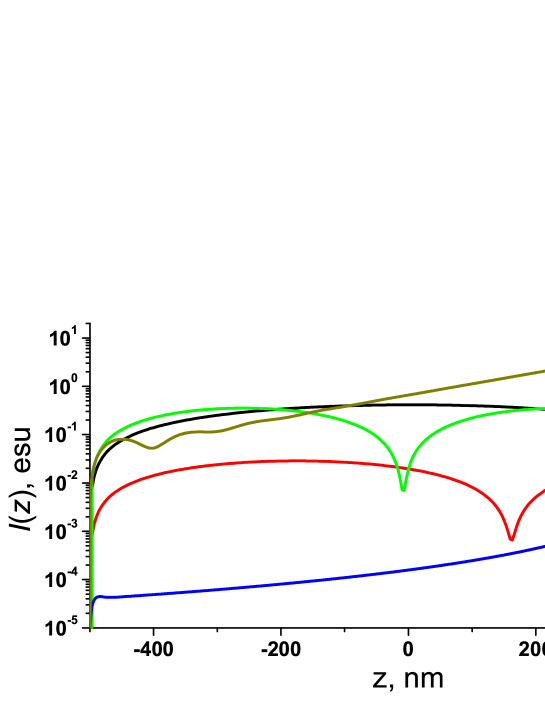
The profiles of the surface current induced in the SWNT by a source electric dipole placed at the centroid of the SWNT ( nm) are presented in Fig. 6. These profiles resemble the ones in Fig. 2(a) for the electric dipole placed at nm. However, we observe much more prominent rise in the induced surface current in the parts of the SWNT close to the source electric dipole in the former case due to the higher strength of the incident electric field at the SWNT surface.
4 Resonant coupling in the near-field zone
The edge conditions affect not only the profile but also the magnitude of the induced surface current, the latter being captured by the average induced surface current
| (21) |
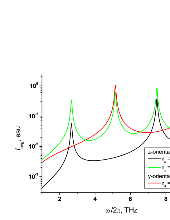
The computed spectra of presented in Fig. 7 contain several resonances at the frequencies defined by the condition , where depends on the location and the orientation of the source electric dipole. When the electric dipole is situated near an edge of the SWNT, is an integer; when the electric dipole is located equally distant from both edges of the SWNT, is either even or odd, depending on the orientation of the electric dipole.
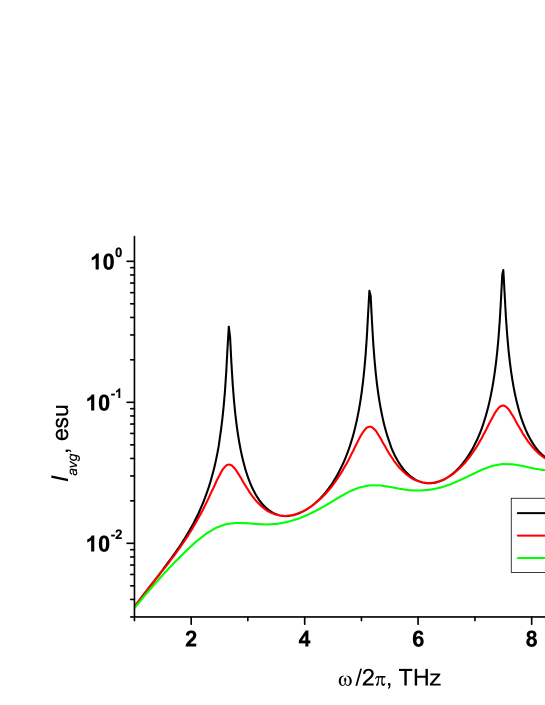
Even though the resonant amplitudes of in Fig. 7 depend on the location and the orientation of the source electric dipole, the full width at half maximum (FWHM) of each resonance is primarily defined not by the source characteristics but by the attenuation of surface waves in the SWNT. This attenuation emerges in our model through the relaxation time that affects the axial surface conductivity of the SWNT. In order to demonstrate the effect of , we present the spectra of for different values of in Fig. 8. A decrease in weakens the resonances but does not drastically affect the off-resonance values of . The dissipation of the surface waves becomes so high for fs that the resonances disappear.
It may seem from Figs. 2 and 3 that the maximum value of the induced surface current grows with the frequency and, in general, is much higher at optical frequencies [cases (iv) and (v)] than at terahertz frequencies [cases (i)–(iii)]. However, this is not so. The spectrum of is presented in Fig. 9(a) for a SWNT when a source electric dipole esu is located at nm. The spectrum of the magnitude of the axial surface conductivity of the same SWNT is presented in Fig. 9(b), wherein we can identify two different spectral regimes: a Drude regime (frequencies THz) and a regime of interband transitions (frequency THz). These two regimes are separated by a strong dip (around THz). The spectral characteristics of are completely different in these two spectral regimes. In the low-frequency regime, varies non-monotonically with frequency even though does. In particular we observe a number of resonant lines in the spectrum of that are the geometrical resonances of the surface plasmons—the same as in Fig. 7. In the low-frequency regime ( THz) except for exactly at the resonance frequencies, is smaller than at the optical resonance frequencies. In the high-frequency regime, the frequency dependence of follows the frequency dependence of ; in particular, two poles due to interband transitions are clearly seen in both spectra.

To explain the spectral dependence of , we should take into account that, according to Eq. (13), the induced surface current density in the SWNT arises from the superposition of two electric fields; i.e.,
| (22) |
where the second term within the square brackets on the right side is the electric field of a surface wave and is defined by Eq. (14). The nonmonotonic dependence of on in the low-frequency regime in Fig. 9 is because the electric field of the surface wave depends on the axial surface conductivity too.
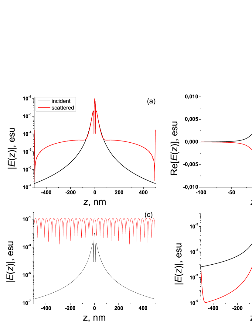
Let us recall that
| (23) |
Plotted in Fig. 10 are the -directed components of the incident and the scattered electric fields on the surface of a SWNT illuminated by an electric dipole of moment esu located at nm. At the frequency ( THz) of the first geometric resonance in the portion of the SWNT close to the source electric dipole, the -directed components of the incident and the scattered electric fields are of similar magnitude; see Fig. 10(a). However, as the real parts of the -directed components of the two fields differ in sign—see Fig. 10(b)—the total electric field on the surface of the SWNT is small, leading to small despite the high magnitude of the axial surface conductivity. As the frequency rises, the scattered electric field on the surface of the SWNT rises (especially at the geometrical resonances frequencies), as shown in Fig. 10(c), and leads to higher despite a lowering of the surface axial conductivity. In the high-frequency regime, the magnitude of the axial surface conductivity is rather low (except for the interband transitions) and the surface wave is strongly damped, the scattered electric field is generally much weaker in strength than the incident electric field, as shown in Fig. 10(d); hence, does not depend on the scattered field.
5 Scattered electric field
5.1 Scattered electric field near the SWNT
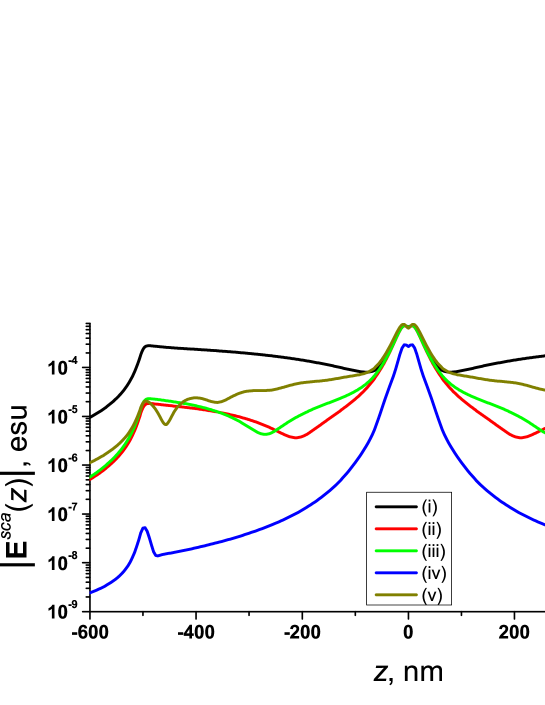
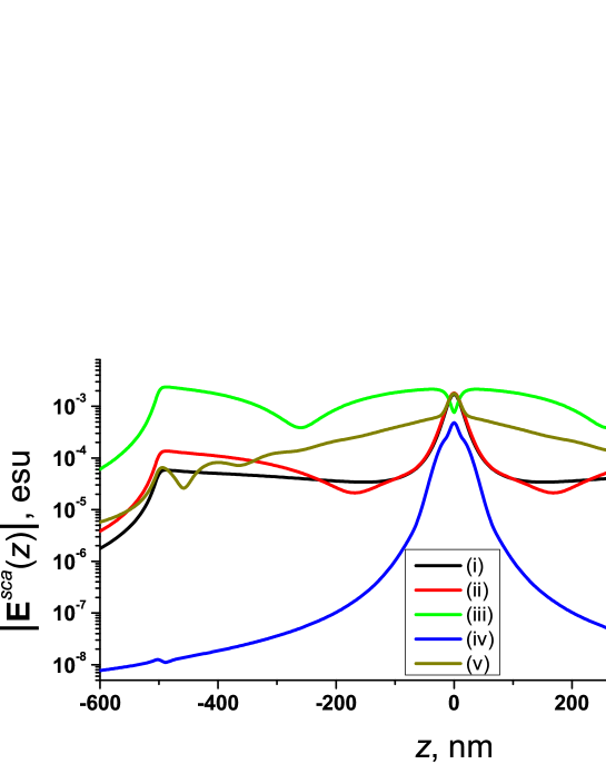
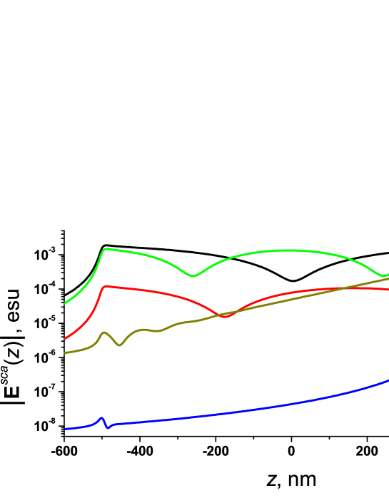
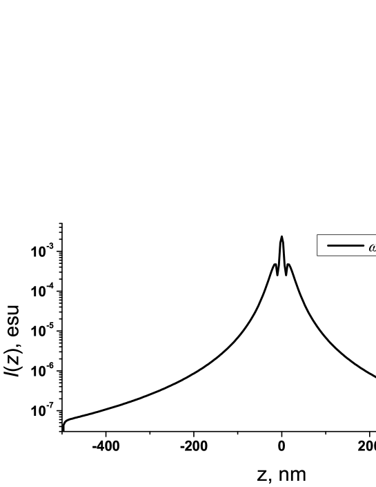
The scattered electric field in the vicinity of the SWNT was calculated using Eq. (10) for all five cases, and two locations and two orientations (as appropriate) of the source electric dipole. Figures 11 and 12 show for nm, .
Substantial enhancement of the maximum value with increasing frequency is not evident in Figs. 11 and 12. However, those figures do offer evidence of the effect of dipole orientation on the scattered electric field. The plots in Figs. 11 and 12 demonstrate that there are two spatial regions wherein the scattered field is localized: (i) close to the source electric dipole and (ii) near the edges of the SWNT. The localization of the field scattered by the SWNT in the region close to source electric dipole could be used in SNOM for the excitation of strongly localized electric fields caused by the spontaneous decay of an emitter placed in the vicinity of an SWNT.
5.2 Radiation patterns of the dipole-SWNT system
Let us now consider the electromagnetic field in the far zone, with direct contribution from the source electric dipole and indirect contribution from the scattered field due to the presence of the SWNT. For this purpose, we chose a spherical coordinate system with origin located at the centroid of the SWNT. We define the joint radiation pattern
| (24) |
at distances far from the dipole-SWNT system.
Equation (10) yields
| (25) |
which does not depend on , whereas Eq. (19) yields
| (26) |
When , Eq. (26) simplifies to
| (27) |
when , we get
| (28) |
Let us examine the function when the source electric dipole is oriented parallel to the SWNT axis and is located on the SWNT axis (i.e., ); then,
| (29) |
is independent of . Displayed in Fig. 13 are polar plots of the normalized joint radiation pattern
| (30) |
in any plane to which the axis is tangential—for and nm, and for the five different cases (i)–(v) delineated in Sec. 3.
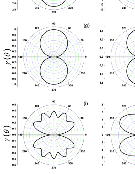
In general, the plots of the normalized joint radiation pattern presented in Fig. 13 for a (15,0) and (18,0) SWNT do not have the form expected of radiation from point electric dipoles. The condition for having the dipolar form—as in Figs. 13(a)-(e)—is , which means that the second term on the right side of Eq. (30) can be ignored. But that is not enough. Indeed, in case (iii) for the source electric dipole placed near an edge of the SWNT edge, Fig. 13(f) does not have the dipolar form even though the condition obviously holds true. Let us study this case in more detail.
Shown in Fig. 14 the induced surface current density on a (15,0) SWNT at 5.2 THz when esu and nm. Whereas the magnitude of is symmetric with respect to the center plane , the argument is asymmetric. The integral on the right side of Eq. (30) is therefore almost null valued for and is small. However, for the phase of the integrand changes due to the presence of , and the joint radiation pattern is enhanced. As the right side of Eq. (30) contains terms proportional to and , radiation lobes centered about appear.

At sufficiently high frequencies, the condition does not hold. However, we still observe the dipolar radiation pattern in Figs. 13(g,h) for case (iv). When the source electric dipole is placed at the centroid of the SWNT, as for Fig. 13(g), the main contribution to the normalized joint radiation pattern is from the first term on the right side of Eq. (30). That term is manifestly dipolar. Scattering by the SWNT is small in the high-frequency regime, due to the strong damping of the surface wave, leading to ohmic absorption rather than reradiation. In contrast, when the source electric dipole is placed near one edge of the SWNT, neither of the two terms on the right side of Eq. (30) is dominant. But the normalized joint radiation pattern in Fig. 13(h) is still dipolar because, as the induced current is confined largely to the edge close to the source electric dipole, that edge acts like an additional electric dipole. Accordingly, we conclude that the presence of an SWNT does not lead to PL enhancement at optical frequencies—in good agreement with the experimental results where strong luminescence quenching for Gd-Se quantum dots and polystyrene spheres in the presence of SWNTs has been observed [41].
Figures 13(i,j) indicate that the joint radiation pattern of the dipole-SWNT system is very different from that of the dipole alone, in case (v). This happens because the chosen frequency is a plasmon resonance frequency.
The normalized joint radiation patterns presented in Fig. 13 also demonstrate the crucial influence of the edges of the SWNT on PL enhancement. At all frequencies the far-field radiation intensity is much higher when the source electric dipole is placed near an edge of SWNT (right column in Fig. 13) than at the centroid of the SWNT (left column in Fig. 13). A strong enhancement by a factor is predicted at the frequency of the first geometrical resonance, i.e., case (i).
5.3 Resolution with an SWNT tip for sSNOM
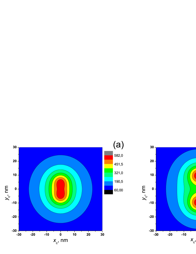
As stated in Sec. 1, the formalism presented in this paper can be applied for sSNOM investigations of a PL object using an SWNT tip. In order to exemplify that assertion, we fixed a (15,0) SWNT of length m on the axis with the centroid of the SWNT serving as the origin of the coordinate system, varied the location nm of the source electric dipole of moment esu radiating at 2.6 THz frequency, and computed as a function of and for both and . The resulting contour plots are presented in Fig. 15.
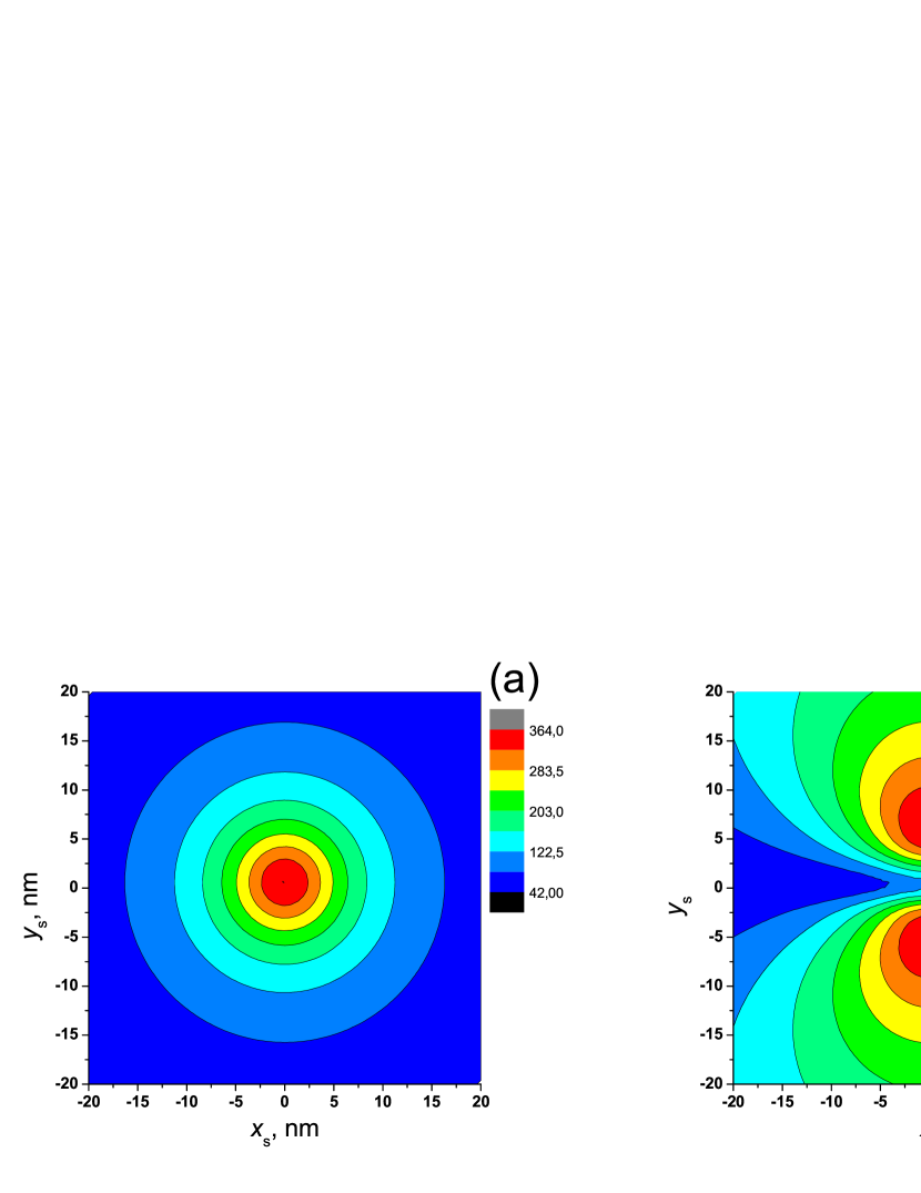
When the electric dipole is oriented along the SWNT axis, the contour plot of the joint radiation pattern in Fig. 15a is a set of concentric circles centered on the SWNT axis. The jointly radiated field decreases in strength rapidly: within nm from the SWNT axis, there is a drop in magnitude by one order. When the electric dipole is oriented normal the SWNT axis, the contour plot in Fig. 15b shows two images arranged symmetrically with respect the plane formed by the SWNT axis and the direction normal to both the SWNT axis and the orientation of the electric dipole. The two images arise due to the weak coupling of -oriented dipole with the SWNT when the distance between the two is small.
In order to study the spatial resolution of the SWNT tip as a probe, the calculations for Fig. 15 were repeated but with two -oriented electric dipoles, one placed at and the other at , where nm is the radius-vector of the two dipoles system geometrical center, and are the interdipole separations along the and -axis respectively. In the contour plots presented in Fig. 16, the two electric dipoles cannot be resolved when the inter-dipole separation is nm. However, resolution is possible when that separation is nm, leading us to the conclusion that spatial resolution of the SWNT-based probe could be between 10 and 20 nm.
6 Concluding remarks
Following a standard procedure, we formulated a Fredholm integral equation for the surface current density induced on a metallic SWNT irradiated by the electromagnetic field of an arbitrary source located outside the SWNT. The integral equation was solved numerically and then used to compute the scattered field. Though we chose the source to be a point electric dipole for numerical work, the technique can be used for other sources such as electrically small loop antennas [19] and even extended sources such as aperture antennas [42].
The relative location and orientation of the source electric dipole influence the profile of the current induced in the SWNT as well as the scattered electric field in the vicinity of the SWNT. This effect can be accentuated by the resonant excitation of a surface wave on the SWNT. We proved this by investigating the frequency dependence of the induced current. Strong spatial localization of scattered electric field near one or both edges of the SWNT, particularly under nonresonant conditions, should promote the adoption of SWNT tips for scanning near-field optical microscopy.
Carbon nanotubes are strongly nonlinear, the nonlinearity becoming substantial when the incident power density is on the order of W cm-2 or larger [43]. For a gaussian pulse, this power density corresponds to a peak electric field on the order of V cm-1, which is three orders of magnitude lower than the atomic field. This value of the electric field strength is of the same order of magnitude as the electric field strength at a distance of nm from the electric dipole—see Eq. (19)—with dipole moment D esu which is the typical value of the dipole moment of a quantum dot [44]. Thus, though the power density in the near-field region can be quite low, the electric field strength can be high enough such that nonlinear effects become significant. Thus, a comprehensive description of the scattering of a near field by an SWNT will lead to the development of near-field nonlinear optics of SWNTs.
Acknowledgments
This research was partially supported by the International Bureau BMBF (Germany) under project BLR 08/001, the Belarus Republican Foundation for Fundamental Research (BRFFR) under project F09MC-009 and EU FP7 CACOMEL project FP7-247007. AL thanks the Charles Godfrey Binder Endowment at Penn State for partial financial support of his research activities. The work of AMN was supported by the BRFFR young scientists grant F09M-071.
References
- [1] J.-C. Charlier, X. Blase, and S. Roche, “Electronic and transport properties of carbon nanotubes,” Rep. Mod. Phys. 79, 677–732 (2007) [doi:10.1103/RevModPhys.79.677].
- [2] J.-P. Salvetat, J.-M. Bonard, N. H. Thomson, A.J. Kulik, L. Forró, W. Benoit, and L. Zuppiroli, “Mechanical properties of carbon nanotubes,” Appl. Phys. A 69, 255–260 (1999) [doi:10.1007/s003399900114].
- [3] P. Avouris, M. Freitag, and V. Perebeinos, “Carbon-nanotube photonics and optoelectronics,” Nature Photon. 2, 341–350 (2008) [doi:10.1038/nphoton.2008.94].
- [4] S. A. Maksimenko, G. Ya. Slepyan, K. G. Batrakov, A. A. Khrushchinsky, P. P. Kuzhir, A. M. Nemilentsau, and M. V. Shuba, “Electromagnetic waves in carbon nanostructures,” in Carbon Nanotubes and Related Structures, V. Blank and B. Kulnitskiy, Eds., pp. 147–187, Research Signpost, Kerala, India (2008).
- [5] C. Rutherglen and P. Burke, “Nanoelectromagnetics: Circuit and electromagnetic properties of carbon nanotubes,” Small 5, 884–906 (2009) [doi:10.1002/smll.200800527].
- [6] L. Novotny and B. Hecht, Principles of Nano-optics, Cambridge University Press, Cambridge, United Kingdom (2006).
- [7] S. Reich, C. Thomsen, and J. Maultzsch, Carbon Nanotubes: Basic Concepts and Physical Properties, Wiley-VCH, Weinheim, Germany (2004).
- [8] V. A. Margulis and T. A. Sizikova, “Theoretical study of third-order nonlinear optical response of semiconductor carbon nanotubes,” Physica B 245, 173–189 (1998) [doi:10.1016/S0921-4526(97)00676-5].
- [9] Y. C. J. Wang and W. J. Blau, “Carbon nanotubes and nanotube composites for nonlinear optical devices,” J. Mater. Chem. 19, 7425–7443 (2009) [doi:10.1039/b906294g].
- [10] Y.-C. Chen, N. R. Raravikar, L. S. Schadler, P. M. Ajayan, Y.-P. Zhao, T.-M. Lu, G.- C. Wang, and X.-C. Zhang, “Ultrafast optical switching properties of single-wall carbon nanotube polymer composites at 1.55 m,” Appl. Phys. Lett. 81, 975–977 (2002) [doi:10.1063/1.1498007].
- [11] G. W. Hanson, “Fundamental transmitting properties of carbon nanotube antennas,” IEEE Trans. Antennas Propagat. 53, 3426–3435 (2005) [doi:10.1109/TAP.2005.858865].
- [12] P. J. Burke, S. Li, and Z. Yu, “Quantitative theory of nanowire and nanotube antenna performance,” IEEE Trans. Nanotechnol. 5, 314–334 (2006) [doi:10.1109/TNANO.2006.877430].
- [13] G. Ya. Slepyan, M. V. Shuba, S. A. Maksimenko, and A. Lakhtakia, “Theory of optical scattering by achiral carbon nanotubes and their potential as optical nanoantennas,” Phys. Rev. B 73, 195416 (2006) [doi:10.1103/PhysRevB.73.195416].
- [14] M. V. Shuba, G. Ya. Slepyan, S. A. Maksimenko, C. Thomsen, and A. Lakhtakia, “Theory of multiwall carbon nanotubes as waveguides and antennas in the infrared and the visible regimes,” Phys. Rev. B 79, 155403 (2009) [doi:10.1103/PhysRevB.79.155403].
- [15] M. V. Shuba, G. Ya. Slepyan, S. A. Maksimenko, C. Thomsen, and A. Lakhtakia, “Electromagnetic wave propagation in an almost circular bundle of closely packed metallic carbon nanotubes,” Phys. Rev. B 76, 155407 (2007) [doi:10.1103/PhysRevB.76.155407].
- [16] Y. Wang, K. Kempa, G. Benham, W. Z. Li, T. Kempa, J. Rybczynski, A. Herczynski, and Z. F. Ren, “Receiving and transmitting light-like radio waves: Antenna effect in arrays of aligned carbon nanotubes,” Appl. Phys. Lett. 85, 2607–2609 (2004) [doi:10.1063/1.1797559].
- [17] J. Hao and G. W. Hanson, “Optical scattering from a planar array of finite-length metallic carbon nanotubes,” Phys. Rev. B 75, 165416 (2007) [doi:10.1103/PhysRevB.75.165416].
- [18] K. Jensen, J. Weldon, H. Garcia, and A. Zettl, “Nanotube radio,” Nano Lett. 7, 3508–3511 (2007) [doi:10.1021/nl0721113]; correction: 8, 374 (2008) [doi:10.1021/nl073089g].
- [19] A. Lakhtakia, M. F. Iskander, C. H. Durney, and H. Massoudi, “Irradiation of prolate spheroidal models of humans and animals in the near field of a small loop antenna,” Radio Sci. 17, 77S–84S (1982) [doi:10.1029/RS017i05Sp0077S].
- [20] A. Lakhtakia, M. F. Iskander, C. H. Durney, and H. Massoudi, “Absorption characteristics of prolate spheroidal models exposed to the near fields of electrically small apertures,” IEEE Trans. Biomed. Eng. 29, 569–576 (1982) [doi:10.1109/TBME.1982.324986].
- [21] G. W. Hanson and P. Smith, “Modeling the optical interaction between a carbon nanotube and a plasmon resonant sphere,” IEEE Trans. Antennas Propagat. 55, 3063–3069 (2007) [doi:10.1109/TAP.2007.908555].
- [22] A. M. Nemilentsau, G. Ya. Slepyan, and S. A. Maksimenko, “Thermal radiation from carbon nanotubes in the terahertz range,” Phys. Rev. Lett. 99, 147403 (2007) [doi:10.1103/PhysRevLett.99.147403].
- [23] R. Hillenbrand, F. Keilmann, P. Hanarp, D. S. Sutherland, and J. Aizpurua, “Coherent imaging of nanoscale plasmon patterns with a carbon nanotube optical probe,” Appl. Phys. Lett. 83, 368–370 (2003) [doi:10.1063/1.1592629].
- [24] W. L. Chan, J. Deibel, and D. M. Mittleman, “Imaging with terahertz radiation,” Rep. Prog. Phys. 70, 1325–1379 (2007) [doi:10.1088/0034-4885/70/8/R02].
- [25] H.-T. Chen, R. Kersting, and G. C. Cho, “Terahertz imaging with nanometer resolution,” Appl. Phys. Lett. 83, 3009–3011 (2003) [doi:10.1063/1.1616668].
- [26] A. Thoma and T. Dekorsy, “Influence of tip-sample interaction in a time-domain terahertz scattering near field scanning microscope,” Appl. Phys. Lett. 92, 251103 (2008) [doi:10.1063/1.2949858].
- [27] A. J. Huber, F. Keilmann, J. Wittborn, J. Aizpurua, and R. Hillenbrand, “Terahertz near-field nanoscopy of mobile carriers in single semiconductor nanodevices,” Nano Lett. 8, 3766–3770 (2008). [doi:10.1021/nl802086x].
- [28] L. G. Cancado, A. Jorio, A. Ismach, E. Joselevich, A. Hartschuh, and L. Novotny, “Mechanism of near-field Raman enhancement in one-dimensional systems,” Phys. Rev. Lett. 103, 186101 (2009) [doi:10.1103/PhysRevLett.103.186101].
- [29] D. Shi, Y. Guo, Z. Dong, J. Lian, W. Wang, G. Liu, L. Wang, and R. C. Ewing, “Quantum-dot-activated luminescent carbon nanotubes via a nano scale surface functionalization for in vivo imaging,” Adv. Mater. 19, 4033–4037 (2007) [doi:10.1002/adma.200700035].
- [30] Z. Zhou, H. G. Kang, M. L. Clarke, S. H. De Paoli Lacerda, M. Zhao, J. A. Fagan, A. Shapiro, T. Nguyen, and J. Hwang, “Water-soluble DNA-wrapped single-walled carbon-nanotube/quantum-dot complexes,” Small 5, 2149–2155 (2009) [doi:10.1002/smll.200801932].
- [31] W. Wang, G. Liu, H. Cho, Y. Guo, D. Shi, J. Lian, and R. Ewing, “Surface charge induced Stark effect on luminescence of quantum dots conjugated on functionalized carbon nanotubes,” Chem. Phys. Lett. 469, 149–152 (2009) [doi:10.1016/j.cplett.2008.12.065].
- [32] H. C. Chen, Theory of Electromagnetic Waves: A Coordinate-Free Approach, McGraw–Hill, New York, USA (1983).
- [33] G. Ya. Slepyan, S. A. Maksimenko, A. Lakhtakia, O. Yevtushenko, and A. V. Gusakov, “Electrodynamics of carbon nanotubes: Dynamic conductivity, impedance boundary conditions, and surface wave propagation,“ Phys. Rev. B 60, 17136–17149 (1999) [doi:10.1103/PhysRevB.60.17136].
- [34] G. Ya. Slepyan, N. A. Krapivin, S. A. Maksimenko, A. Lakhtakia, and O. M. Yevtushenko, “Scattering of electromagnetic waves by a semi-infinite carbon nanotube,” Arch. Elektron. Über. 55, 273–280 (2001) [doi:10.1078/1434-8411-00041].
- [35] S. Ström, “Introduction to integral representations and integral equations for time-harmonic acoustic, electromagnetic and elastodynamic wave fields,” in Field Representations and Introduction to Scattering, V. V. Varadan, A. Lakhtakia, and V. K. Varadan, Eds., pp. 37–141, North–Holland, Amsterdam, The Netherlands (1991).
- [36] G. Ya. Slepyan, S. A. Maksimenko, A. Lakhtakia, O. M. Yevtushenko, and A. V. Gusakov, “Electronic and electromagnetic properties of carbon nanotubes,” Phys. Rev. B 57, 9485–9497 (1998) [doi:10.1103/PhysRevB.57.9485].
- [37] G. Arfken, Mathematical Methods for Physicists, 3rd ed., Academic Press, Orlando, FL, USA (1985).
- [38] J. N. Farahani, D. W. Pohl, H.-J. Eisler, and B. Hecht, “Single quantum dot coupled to a scanning optical antenna: a tunable superemitter,” Phys. Rev. Lett. 95, 017402 (2005) [doi:10.1103/PhysRevLett.95.017402].
- [39] L. Van Hove, “The occurrence of singularities in the elastic frequency distribution of a crystal,” Phys. Rev. 89, 1189–1193 (1953) [doi:10.1103/PhysRev.89.1189].
- [40] F. Bassani and G. Pastori Parravicini, Electronic States and Optical Transitions in Solids, Pergamon Press, Oxford, United Kingdom (1975).
- [41] C. Mu, B. D. Mangum, C. Xie, and J. M. Gerton, “Nanoscale fluorescence microscopy using carbon nanotubes,” IEEE Sel. Top. Quantum Electron. 14, 206–216 (2008) [doi:10.1109/JSTQE.2008.912914].
- [42] P. J. Wood, “Spherical waves in antenna problems,” Marconi Rev. 34, 149–172 (1971).
- [43] C. Stanciu, R. Ehlich, V. Petrov, O. Steinkellner, J. Herrmann, I. V. Hertel, G. Ya. Slepyan, A. A. Khrutchinski, S. A. Maksimenko, F. Rotermund, E. E. B. Campbell, and F. Rohmund, “Experimental and theoretical study of third-order harmonic generation in carbon nanotubes,“ Appl. Phys. Lett. 81, 4064–4066 (2002) [doi:10.1063/1.1521508].
- [44] K. L. Silverman, R. P. Mirin, S. T. Cundiff, and A. G. Norman, “Direct measurement of polarization resolved transition dipole moment in InGaAs/GaAs quantum dots,” Appl. Phys. Lett. 82, 4552-4554 (2003) [doi:10.1063/1.1584514].
![[Uncaptioned image]](/html/1003.4746/assets/x19.png)
Andrei M. Nemilentsau received his M.S. in theoretical physics in 2004 from Belarus State University (BSU), Minsk, Belarus, and his Ph.D. in theoretical physics in 2009 from the Institute of Physics, Belarus National Academy of Sciences, Minsk, Belarus. Currently he is working as a scientific researcher in the Laboratory of Electrodynamics of Nonhomogeneous Media at the Institute for Nuclear Problems, BSU. His current research interests are the electromagnetic processes in nanostructures. Dr. Nemilentsau is a recipient of the World Federation of Scientists Scholarship for Young Scientists (2003) and the INTAS Young Scientist Fellowship for Ph.D. Students (2006).
![[Uncaptioned image]](/html/1003.4746/assets/x20.png)
Gregory Ya. Slepyan received his M.S. in radioengineering in 1974 from Minsk Institute of Radioengineering, Minsk, Belarus; his Ph.D. in radiophysics in 1979 from Belarus State University (BSU), Minsk, Belarus; and his D.Sc. in radiophysics in 1988 from Kharkov State University, Kharkov, Ukraine. Since 1992 he has been working as a principal researcher of the Laboratory of Electrodynamics of Nonhomogeneous Media at the Institute for Nuclear Problems, BSU. He has authored or coauthored 2 books, 4 collective monographs, and more than 200 conference and journal papers. He is the Member of Editorial board of the journal Electromagnetics. His current research interests are high-power microwave vacuum electronics, antennas and microwave circuits, mathematical theory of diffraction, nonlinear oscillations and waves, nanophotonics and nano-optics (including electrodynamics of carbon nanotubes and quantum dots).
![[Uncaptioned image]](/html/1003.4746/assets/x21.png)
Sergei A. Maksimenko received his M.S. in physics of heat and mass transfer in 1976 and his Ph.D. in theoretical physics in 1988, both from Belarus State University (BSU), Minsk, Belarus, and his D.Sc. in theoretical physics in 1996 from the Institute of Physics, Belarus National Academy of Sciences, Minsk, Belarus. Since 1992 he has been working as head of the Laboratory of Electrodynamics of Nonhomogeneous Media at the Institute for Nuclear Problems (INP), BSU. He also teaches at the BSU physics department. He was the deputy director of INP from 1997 to 2000, and a deputy vice-president of BSU from 2000 to 2005. He has authored or coauthored more than 150 conference and journal papers. In 2003, 2004 and 2006 years he co-chaired conferences as parts of SPIE’s 48th and 49th Annual Meetings, and SPIE’s Optics and Photonics. He is an associate editor of Journal of Nanophotonics and an SPIE Fellow. His current research interests are electromagnetic wave theory and electromagnetic processes in quasi-one- and zero-dimensional nanostructures in condensed matter.
![[Uncaptioned image]](/html/1003.4746/assets/x22.png)
Akhlesh Lakhtakia received degrees from the Banaras Hindu University (B.Tech. & D.Sc.) and the University of Utah (M.S. & Ph.D.), in electronics engineering and electrical engineering, respectively. He is the Charles Godfrey Binder (Endowed) Professor of Engineering Science and Mechanics at the Pennsylvania State University. He is a Fellow of SPIE, Optical Society of America, American Association for the Advancement of Science, and Institute of Physics (UK). He is presently the editor-in-chief of Journal of Nanophotonics. His current research interests include nanotechnology, plasmonics, complex materials, metamaterials, and sculptured thin films.
![[Uncaptioned image]](/html/1003.4746/assets/x23.png)
Slava V. Rotkin is the Frank J. Feigl Junior Faculty Scholar and Assistant Professor of Physics at Lehigh University, Bethlehem, PA. He received his M.Sc. (Summa Cum Laude) in 1994 from the Electro-technical University and his Ph.D. in 1997 from Ioffe Institute (both in St. Petersburg, Russia). Dr. Rotkin is a recipient of scientific awards, including: Libsch Early Career Research Award (2007), Feigl Scholarship (2004), Beckman Fellowship (2000), Royal Swedish Academy of Sciences Fellowship (1995), and President’s Grant for Young Scientists of Russia (1994).