Anisotropic structural and optical properties of -plane AlInN nearly-lattice-matched to GaN
Abstract
We report epitaxial growth of -plane AlInN layers nearly-lattice-matched to GaN. Unlike for -plane oriented epilayers, -plane Al1-xInxN cannot be simultaneously lattice-matched to GaN in both in-plane directions. We study the influence of temperature on indium incorporation and obtain nearly-lattice-matched Al0.81In0.19N at a growth temperature of . We outline a procedure to check in-plane lattice mismatch using high resolution x-ray diffraction, and evaluate the strain and critical thickness. Polarization-resolved optical transmission measurements of the Al0.81In0.19N epilayer reveal a difference in bandgap of meV between (electric field) Ec -axis and conditions with room-temperature photoluminescence peaked at eV strongly polarized with , in good agreement with strain-dependent band-structure calculations.
pacs:
Valid PACS appear hereIn the [0001] -plane orientation, AlInN (In%) can be perfectly lattice matched to GaN. This, along with a large bandgap and high refractive index contrast with GaN makes it ideal for Bragg mirrors, microcavity structures butte ; doraz ; carlin , strain-free transistors, photodetectors, and emitters Medjdoub ; senda . However, to minimize the deleterious effect of spontaneous and piezoelectric polarization fields, growing nitrides along non-polar orientations has advantages, and enables polarization-sensitive optical devices paskova . Epitaxial growth of AlInN is extremely challenging since the optimum growth conditions for AlN and InN are very different, the alloy tends to phase separate and shows composition inhomogeneities Matsuoka ; minj ; hums . Optimized growth of AlInN along the -axis orientation is reported doraz ; carlin ; Medjdoub ; senda ; hums ; fuji . However, the growth mechanisms for non-polar oriented epilayers are different and much less studied. Unlike the -plane case, -plane AlInN can not be grown perfectly lattice-match to GaN. In this letter, we report the synthesis of nearly-lattice-matched -plane Al0.81In0.19N via metalorganic vapor phase epitaxy (MOVPE). The anisotropic structural properties are evaluated from high-resolution x-ray diffraction (HRXRD), and strain and critical thickness estimated. The measured optical properties show a strong polarization anisotropy and are compared with results from band-structure calculations.
All epilayers were grown via MOVPE on -plane sapphire in a close-coupled showerhead reactor using standard precursors. Structural characterization was carried out using a Philips X PERTTM HRXRD system. Optical transmission measurements were performed on backside-polished samples using a Glan-Taylor polarizer on a Cary spectrophotometer. Photoluminescence (PL) measurements were performed using 266 nm laser excitation. The surface morphology was studied by optical and atomic force microscopy.
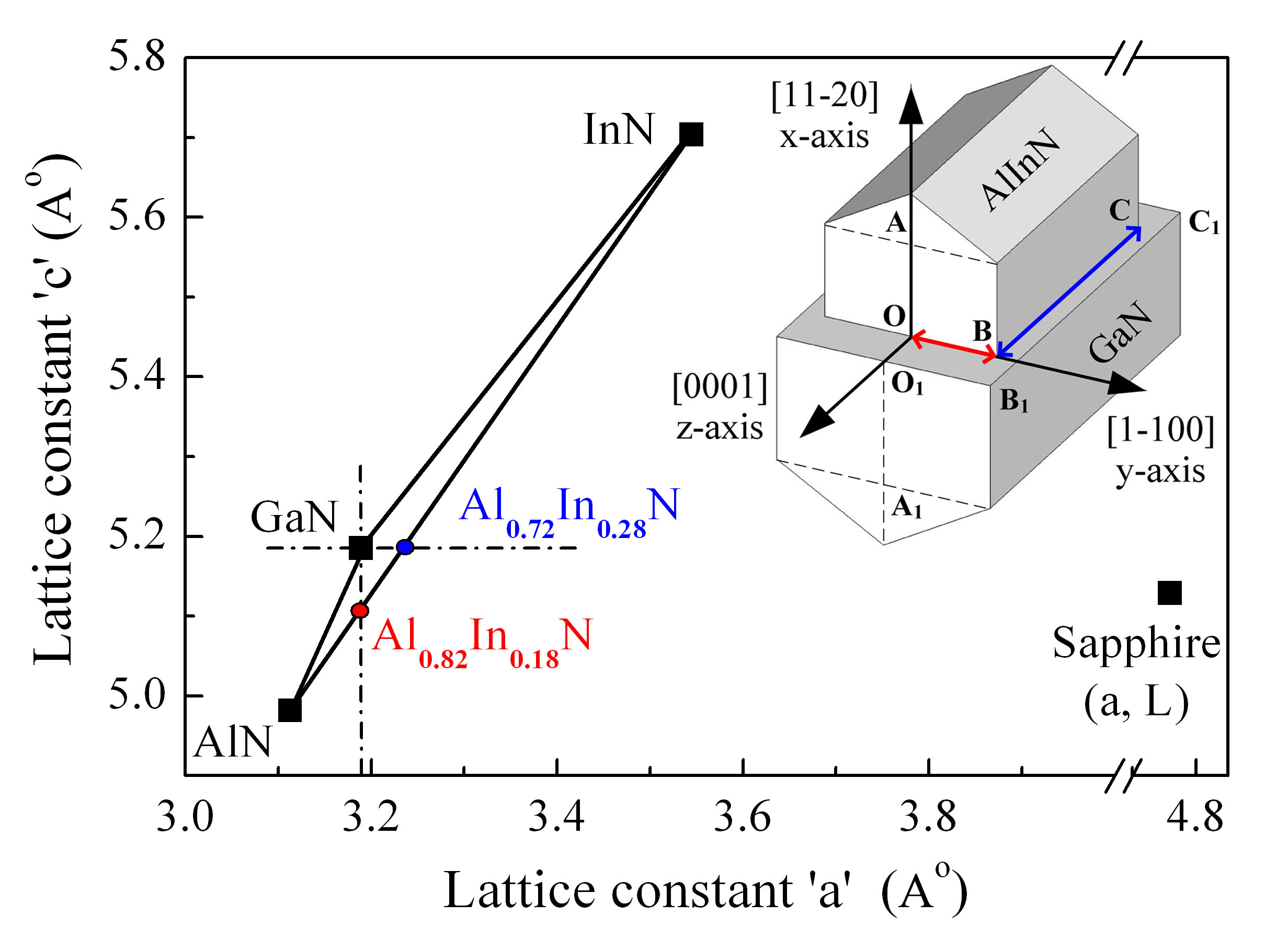
Fig.1 shows the position of relaxed AlN, GaN, InN and sapphire in lattice-parameter space. The ratio of GaN (1.626) is a little higher than that of AlN (1.600) and InN (1.603) angerer ; maleyre , hence for oriented epilayers it is impossible to get perfect lattice matching of AlInN on GaN along both in-plane directions. The inset of Fig.1 shows the relative orientation of the AlInN and GaN unit cells. From Vegard’s Law it can be shown that the Al1-xInxN/GaN system will be lattice-matched along m-axis () for = (i.e. =, but ), whereas lattice-matching along c-axis() requires = (i.e. =, but ).
The indium incorporation into AlInN () depends strongly on growth temperature, and was studied by growing a set of AlInN epilayers on AlN buffer layers over the temperature range at fixed (TMIn/(TMAl+TMIn))=. The was estimated from the , , , and reflections following the procedure in RefmrlLattice (with 1-2% error). As shown in Fig.2, the is close to the -value at . With increasing temperature the desorption of In-atoms from the surface increases, hence reducing solid phase In-incorporation. At high temperature, , typically needed for high quality Al-alloys, is less than %, showing the difficulty of growing AlInN. To obtain 18% (lattice matched to GaN along y-axis), the temperature required is .
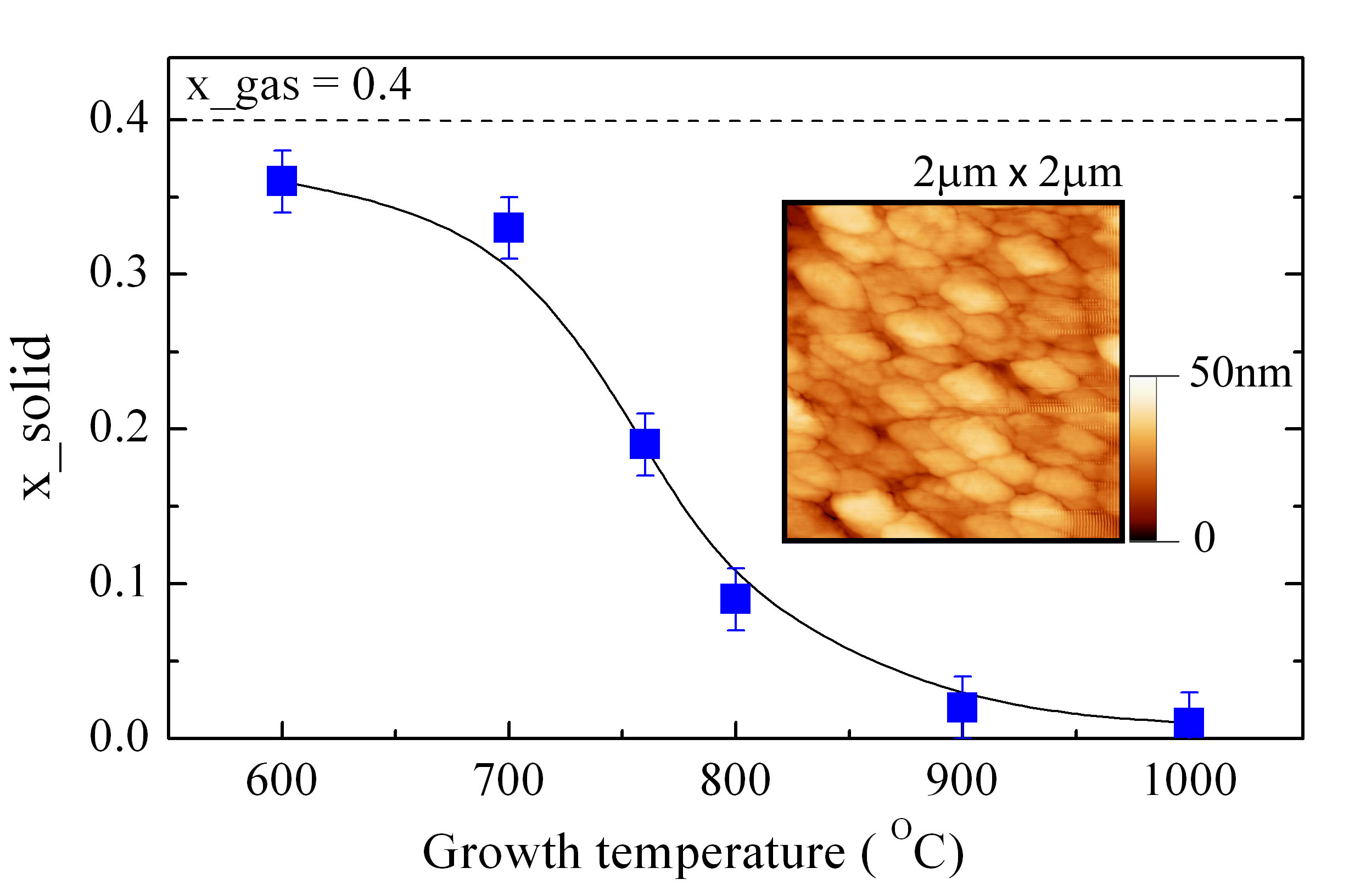
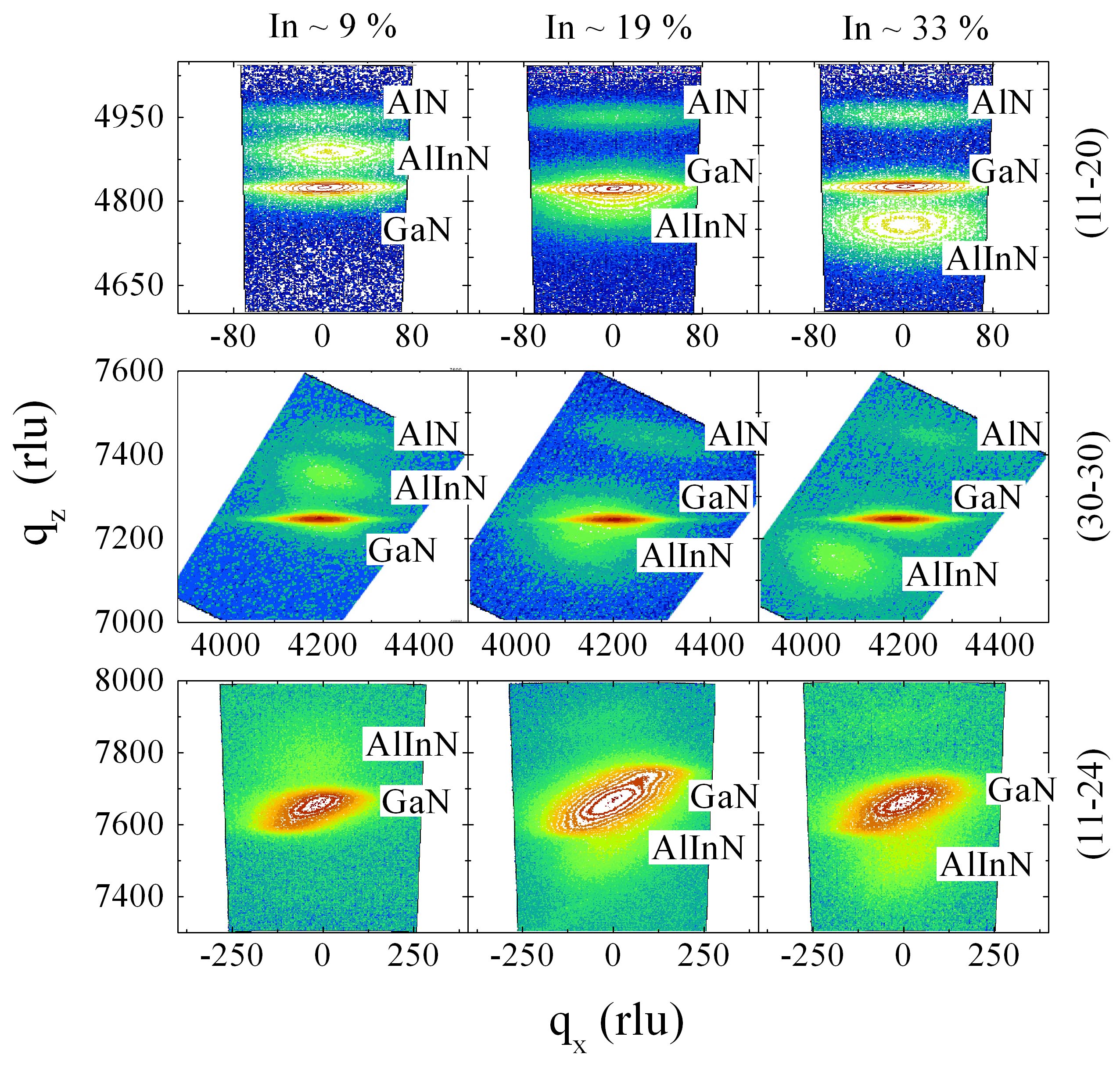
Fig.3 shows a set of reciprocal space maps (RSM) of AlInN epilayers deposited on GaN buffer layer at , and having of %, % and % respectively. Our diffractometer cannot directly probe the and reflections; we hence rely on a combination of symmetric and asymmetric reflections to confirm lattice matching (LM) along different in-plane directions. For an -plane oriented layer the plane is symmetric, hence its lattice point (LP) is on the vertical axis in reciprocal space. To verify LM of AlInN/GaN along the m-axis (Inset:Fig.1), we use the -plane, whose LP lies in a plane both to the c-axis and to the m-axis in reciprocal space. The RSMs shows that the diffraction peak of Al0.81In0.19N epilayer coincides with GaN for the symmetric and asymmetric reflections, confirming LM along m-axis. Similarly to verify LM along the c-axis, we use the reflection, since its reciprocal lattice point lies in a plane both to the m-axis and to the c-axis. The separate peaks of AlInN and GaN indicate that the layer is not LM along the c-axis.
The advantage of growing Al0.81In0.19N on GaN (LM along m-axis) rather than Al0.72In0.28N (LM along c-axis) is that it provides higher refractive index contrast making it more useful for Bragg mirrors. Although Al0.81In0.19N on GaN has nearly zero lattice misfit along m-axis, the strain due to lattice-misfit =% along c-axis can cause cracking beyond a certain critical thickness (). A theoretical estimate matthews ; murray of for Al0.81In0.19N on GaN is nm which is relatively smaller than the nm thickness at which we typically observe cracks.
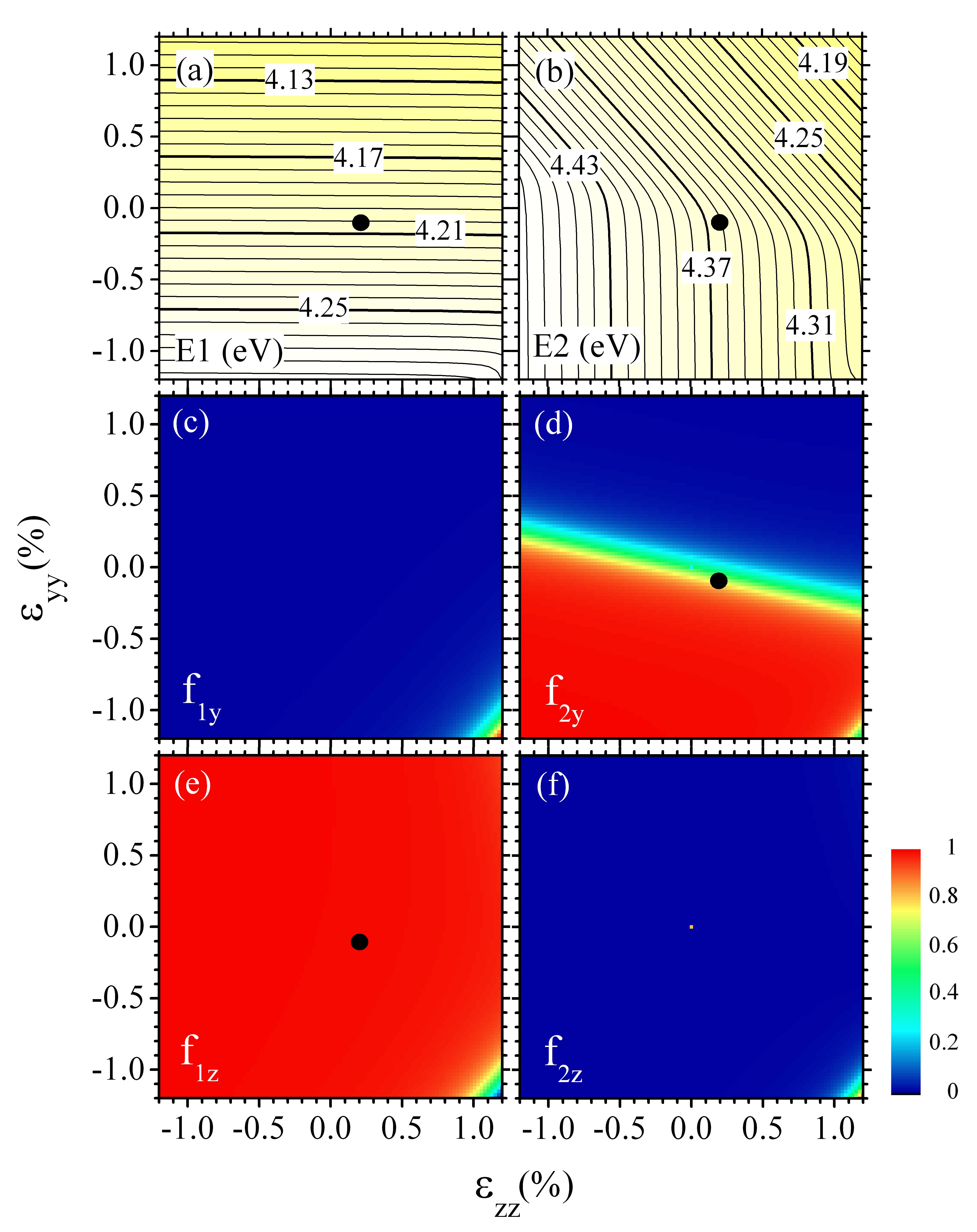
To study the optical properties we use Al0.81In0.19N epilayers grown on transparent AlN buffer layers and measure the bandgap from polarization-resolved optical transmission and PL measurements. Wurtzite group III-nitrides have intrinsic polarization anisotropy in their optical properties sandip . In epitaxial alloys, the composition and in-plane strain causes the mixing of the three upper-most valance bands, which not only changes the transition energies but also modifies the polarization selection rules for each transition. For , we have calculated the three lowest interband transition energies (, , ) and their oscillator strengths (OS) for x, y, z-polarization by solving the Bir-Pikus Hamiltonian ftnote2 . Fig.4 shows the calculated , values and their y, z component of OS as a function of and . Using HRXRD we estimate the in-plane anisotropic strain in our layer as =% and =% (black dots in Fig.4[d-e]), for which transition is strongly z-polarized and transition is predominantly y-polarized.
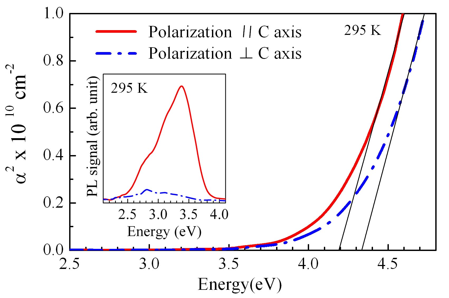
Fig.5 shows the absorption spectra for two different polarizations (electric field) () and () for which the extrapolated bandgaps are eV and eV respectively (which we had assigned as and in our calculation). The measured difference in bandgap = meV agrees well with the theoretical estimate meV (from Fig.4a&b). The Fig.5 inset shows the room temperature PL spectrum which peaks at eV. Such a large Stokes-shift of eV in PL arises because of indium localization and is similar to values observed for -plane epilayers butte ; zhou . The PL spectrum is strongly polarized at as expected because the lowest energy transition has a strong z-polarized OS and very weak y-polarized OS. The UV bandgap of Al0.81In0.19N coupled with its inherently anisotropic optical properties makes it promising for polarization-sensitive detectors and emitters in the UV.
In conclusion, we show it is impossible to achieve perfectly-lattice-matched AlInN on GaN and suggest a method to verify in-plane lattice mismatch. A study of In-incorporation as a function of temperature allows us to obtain nearly-lattice-matched Al0.81In0.19N at . Polarization-resolved optical measurements show a strong anisotropy. Our results would be useful for polarization-sensitive detectors and polarized emitters in the UV, and non-polar AlInN-based Bragg mirrors.
References
- (1) R. Butte, J-F Carlin, et al.. J. Phys. D: Appl. Phys. 40, 6328 (2007).
- (2) J. Dorsaz, J.-F. Carlin, S. Gradecak, M. Ilegems, J. Appl. Phys. 97, 084505 (2005).
- (3) J. F. Carlin, J. Dorsaz, E. Feltin, R. Butte, N. Grandjean, M. Ilegems, Appl. Phys. Lett. 86, 031107 (2005).
- (4) F. Medjdoub, D. Ducatteau, C. Gaquiere, J.-F. Carlin, M. Gonschorek, E. Feltin, M.A. Py, N. Grandjean, E. Kohn, Electron. Lett. 43, 309 (2007).
- (5) S. Senda, H. Jiang, T. Egawa, Appl. Phys. Lett. 92, 203507 (2008).
- (6) T. Paskova, Phys. Stat Sol. (b) 245, 1011 (2010).
- (7) T. Matsuoka, H. Okamoto, M. Nakao, H. Harima, E. Kurimoto, Appl. Phys. Lett. 81, 1246 (2002).
- (8) A. Minj, D. Cavalcoli, A. Cavallini, Appl. Phys. Lett. 97, 132114 (2010).
- (9) C. Hums, J. Blasing, A. Dadgar, A. Diez, T. Hempel, J. Christen, and A. Krost,K. Lorenz, E. Alves, Appl. Phys. Lett. 90, 022105 (2007).
- (10) T. Fujimori, H. Imai, A. Wakahara, H. Okada, A. Yoshida, T. Shibata, M. Tanaka, J. Cryst. Growth 272, 381 (2004).
- (11) H. Angerer, D. Brunner, F. Freudenberg, O. Ambacher, M. Stutzmann, R. Hoepler, T. Metzger, E. Born, G. Dollinger, A. Bergmaier, S. Karsch, H. J. Korner, App. Phys. Lett 71, 1504 (1997).
- (12) B. Maleyre, S. Ruffenach, O. Briot, A. Lee, Superlattices and Microstructures 36, 527 (2004).
- (13) Lattice point of sapphire: =nm and ==nm. The factor arises as one unit cell of sapphire fits three nitride unit cells.
- (14) M. R. Laskar, T. Ganguli, A. A. Rahman, A. Mukherjee, N. Hatui, M. R. Gokhale, A. Bhattacharya, J. Appl. Phys. 109, 013107 (2011) .
- (15) J. W. Matthews, E. Klokholm, Mat. Res. Bull. 7, 213 (1972) .
- (16) R. T. Murray, C. J. Kiely, M. Hopkinson, Phill. Mag. A. 74, 169 (1996) .
- (17) J. Bhattacharya, S. Ghosh, H. T. Grahn, Phys. Status Solidi B 246, 1184 (2009).
- (18) We followed the method suggested by S. Ghosh et al. [Phys. Rev. B 65, 075202 (2002)]. The band structure parameters for AlN and InN are taken from Refsandip and linearly extrapolated for AlInN.
- (19) L. Zhou, D. J. Smith, M. R. McCartney, D. S. Katzer, D. F. Storm, App. Phys. Lett. 90, 081917 (2007) .