Semiconductor saturable absorbers for ultrafast THz signals
Abstract
We demonstrate saturable absorber behavior of n-type semiconductors GaAs, GaP and Ge in THz frequency range at room temperature using nonlinear THz spectroscopy. The saturation mechanism is based on a decrease in electron conductivity of semiconductors at high electron momentum states, due to conduction band nonparabolicity and scattering into satellite valleys in strong THz fields. Saturable absorber parameters, such as linear and non-saturable transmission, and saturation fluence, are extracted by fits to a classic saturable absorber model. Further, we observe THz pulse shortening, and an increase of the group refractive index of the samples at higher THz pulse peak fields.
Semiconductor saturable absorbers and saturable absorber mirrors (SESAMs) are routinely used for ultrafast laser modelocking and ultrafast signal control KELLER_SESAM_1 . Saturable absorbers operating in the visible and infrared wavelength ranges rely on bleaching of two-level electronic systems, usually realized by an interband transition in semiconductor quantum wells or quantum dots Lagatsky_SESAM . Clearly, such quantum-confined semiconductor systems will not be suitable for applications in the far-infrared (THz) range, where the photon energy is much smaller than the bandgap energy of most semiconductors, and where thermal population of such closely spaced electronic levels would dominate. The main loss factor in doped semiconductors in the THz frequency range is free-carrier absorption. The THz signal attenuation is roughly proportional to the conductivity of the material , where is elementary charge, and and are the mobilities and concentrations of electrons and holes, respectively schall_jepsen ; Lui_Hegmann_APL .
In this Letter we demonstrate saturable absorbers for the THz frequency range, based on n-type bulk semiconductors, where the carrier mobility is modulated by nonlinear electron transport caused by the THz electric field, thus affecting the conductivity of the sample. Normally, the application of external electric fields leads to acceleration of carriers in the lowest-energy valley of the conduction band of an n-type semiconductor. At high-momentum states the valley nonparabolicity becomes pronounced, which leads to an increase in the effective mass and thus to a reduction of the mobility , consequently leading to a reduced dielectric loss in the THz range Matze_transp3 . At high enough electric fields, intervalley scattering is possible conwell1967 ; constant1985 , leading to electron transfer into the satellite valleys with reduced curvature. This again results in a smaller electron mobility compared to that of the conduction band minimum, and consequently lower THz dielectric loss. Detailed studies of time-resolved high-THz-field transport in bulk semiconductors were recently published in Refs. Matze_transp1 ; Matze_transp2 ; razzari2009 .
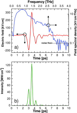
In our experiment, we generated high-power single-cycle THz pulses by tilted pulse-front optical rectification in a lithium niobate crystal of 800-nm, 80-fs laser pulses provided by a 1-kHz repetition rate Ti:Sapphire amplifier Matze_LNB . The THz pulses were collimated and then refocused onto a sample point using a set of off-axis paraboloidal mirrors. After propagation through the sample point, the THz pulses were guided to a 0.5-mm thick undoped 110-oriented ZnTe crystal for detection using standard free-space electro-optic sampling (FEOS) FEOS_Zhang . A pair of wire-grid polarizers was introduced into the THz beam path before the sample point, which allowed us to controllably attenuate the THz signal by adjusting the angle between the polarizer axes. The maximum THz pulse energy was measured to be 1.5 J using a calibrated pyroelectric detector, in the THz beam waist of 1.0 mm (intensity, 1/) at the sample location. This is equivalent to a maximal THz fluence of J/cm2, corresponding to a peak electric field of 300 kV/cm. The peak field was determined by calibrating the squared time-domain electro-optic signal with the known value of pulse fluence. Fig. 1 shows the temporal dependency of electric field as measured by FEOS, the amplitude frequency spectrum, and corresponding instantaneous intensity at the position of the sample of the strongest THz signal used in our experiments. The samples under study were n-type semiconductors: GaAs with a carrier concentration of and a thickness of 0.4 mm; GaP with a carrier concentration of and thickness of 0.3 mm; and Ge with a carrier concentration of and a thickness of 6 mm. The measurements were carried out at room temperature.
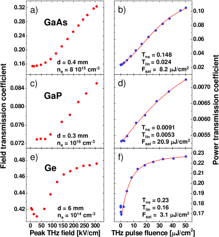
Fig. 2 shows the field and power transmission coefficients as a function of THz pump field and fluence respectively in GaAs, GaP and Ge. The field and power transmission coefficients were obtained by integrating either the modulus or the square, respectively, of the transmitted THz fields transmitted through the sample, and dividing them by reference values recorded without the sample in the beam path. In all our samples we observed increased transmission at higher pump fluences. In particular, we observed a nearly five-fold increase in power transmission coefficient for GaAs sample in the THz pulse fluence range used in our experiments. The solid lines in Figs. 3(b,d,f) are fits using a saturable power transmission function, defined after Ref. Keller_SESAM as
| (1) |
where and are linear and non-saturable power transmission coefficients, is the pump fluence, and is the saturation fluence. Using fits with Eq. 1 we were able to extract the saturable absorber parameters for our semiconductor samples. These parameters, namely linear and non-saturable transmission, and saturation fluence are indicated in Fig. 2. In particular, the saturation fluence was found to be 8.2 J/cm2 for GaAs, 20.9 J/cm2 for GaP, and 3.1 J/cm2 for Ge. Interestingly, at the lowest pump fluences the transmission function for Ge actually decreases slightly, thus demonstrating the opposite, optical limiting behavior. This can be possibly explained by the fact that in Ge the high-mobility -valley is not initially populated, and thus initial sample conductivity is lower, as discussed in Ref. Matze_transp3 .

In all our samples we observed shortening of the THz pulses, as they propagated through the samples, with increase in peak electric field of the THz pulse. Such pulse-shortening behavior is also characteristic for saturable absorbers in the optical range. In order to quantify the shortening of single-cycle THz pulses used in our experiment, we calculated a pulse shortening factor defined as the ratio of full width at half maximum (FWHM) of modulus of Hilbert transforms of sample and reference pulses, as illustrated in Fig. 3(a,b). The dependency of the pulse shortening factor on the peak electric field of the incident THz pulse is shown in Fig. 3(c). For GaP and Ge the maximum relative pulse shortening (i.e. the difference between largest and smallest shortening factors) reaches approximately 5%, and its dependency on THz peak field is more or less linear. For GaAs, however, this dependency appears to have a threshold at THz peak field of around 150 kV/cm and, and the relative pulse shortening reaches the value of approximately 10%.
Saturable absorption and pulse shortening are accompanied by an increase in group refractive index in all three samples, as shown in Fig. 3(d). The group index at various pump intensities was calculated using the difference of arrival times between sample and reference pulses and taking into account the sample thickness by using the relation . The arrival times were obtained from mean-weighted maxima of the modulus of THz pulse Hilbert transforms. We observe a clear saturating growth trend in the group refractive indices of all our samples with increasing THz fields. The most dramatic index growth is observed in GaAs, and it reaches , whereas for Ge it is only in the full THz pulse peak field range available in our experiments. We note that very similar dependencies were obtained if the maxima of THz pulses, and not of the modula of their Hilbert transforms were analyzed.
The observed increase in group index with stronger THz pump is indeed anticipated, and two contributions to this effect are considered. The first contribution is the change in reflectivity at the sample surface schall_jepsen . A decrease in the sample absorption, resulting from the strong THz excitation, leads to a positive phase shift of THz pulse at the interface between the air and absorbing sample. This causes a temporal delay of the transmitted THz pulse and consequently a larger group refractive index. The other contribution to a group index growth with stronger pump stems from the propagation through the bulk of the sample with the phase index dispersion in the frequency range below resonance (in this case - plasma resonance). Larger effective mass , acquired by the carriers at high-momentum states as a result of intense THz excitation, will lead to a decrease in plasma frequency , thus making the frequency dependency of phase index more steep. This would result in the higher value of a group index for the stronger excited samples. The same effect will arise from the effective reduction of the density of highly mobile carriers at the bottom of the -valley. Both interface and bulk contributions to group index growth obviously depend on the strength of the THz excitation and will thus saturate with the overall THz transmission, which is in accordance with our observations. We note that a similar increase in the pulse delay and thus in the group index with stronger optical pump was also observed in saturable absorbers for the optical range, as described in Ref. mork .
We further note that n-type GaP is often used as a broadband FEOS detector, where parasitic etalon reflections of the THz pulses within the crystal are conveniently suppressed by the free-carrier absorption. As we have shown here, in the case of high THz field strengths the results of THz spectroscopy will be distorted due to n-GaP nonlinearities. Therefore, for etalon suppression in high-field experiments it is advisable to use combined active-inactive crystals dmt_combined_xtals instead of doped crystals.
In conclusion, we have observed ultrafast saturable absorption in n-type semiconductors GaAs, GaP, and Ge in the THz range at room temperature. We were able to extract linear and non-saturable transmission coefficients, as well as the saturation fluence using a standard saturable absorber model developed for the optical frequency range. Our data shows THz pulse shortening, and growth of group refractive index of our samples with increase in THz excitation, correlated with the saturating transmission through the samples. Although the origin of the absorption mechanism in the THz and in the optical frequency ranges is completely different, we note that the saturation fluences observed here are within the same order of magnitude (i.e. few to tens of J/cm2), as the values reported for SESAMs in the optical range, such as e.g. quantum dot SESAMs Lagatsky_SESAM ; dmt_QDs_satabs . Optimized THz SESAMs could potentially be used with the THz sources like quantum cascade lasers (QCLs), leading for example to external-cavity mode-locked QCLs delivering high-energy ultrashort THz pulses.
We are grateful to Danish Advanced Technology Foundation (HTF) for financial support; and to A. Cavalleri (Univ. Hamburg), K. Yvind, J. Mørk, and J. M. Hvam (DTU Fotonik) for valuable assistance and discussions. Correspondence should be addressed to M.C.H (matthias.c.hoffmann@desy.de) or D.T. (dmtu@fotonik.dtu.dk).
References
- (1) U. Keller, K. J. Weingarten, F. X. Kärtner, D. Kopf, B. Braun, I. D. Jung, R. Fluck, C. Hönninger, N. Matuschek, and J. A. der Au, IEEE J. Quantum Electron. 2, 435 (1996).
- (2) A. A. Lagatsky, F. M. Bain, C. T. A. Brown, W. Sibbett, D. A. Livshits, G. Erbert, and E. U. Rafailov, Appl. Phys. Lett. 91, 231111 (2007).
- (3) M. Schall and P. U. Jepsen, Opt. Lett. 25, 13 (2000).
- (4) K. P. H. Lui and F. A. Hegmann, Appl. Phys. Lett. 78, 3478 (2001).
- (5) J. Hebling, M. C. Hoffmann, H. Y. Hwang, K.-L. Yeh, and K. A. Nelson, Phys. Rev. B 81, 035201 (2010).
- (6) E. M. Conwell, High Field Transport in Semiconductors, (Academic Press, New York, 1967).
- (7) E. Constant, in Hot Electron Transport in Semiconductors, L. Reggiani, ed. (Springer, 1985).
- (8) M. C. Hoffmann, J. Hebling, H. Y. Hwang, K.-L. Yeh, and K. A. Nelson, Phys. Rev. B 79, 161201R (2009).
- (9) M. C. Hoffmann, J. Hebling, H. Y. Hwang, K.-L. Yeh, and K. A. Nelson, J. Opt. Soc. Am. B 26, A29 (2009).
- (10) L. Razzari, F. H. Su, G. Sharma, F. Blanchard, A. Ayesheshim, H.-C. Bandulet, R. Morandotti, J.-C. Kieffer, T. Ozaki, M. Reid, and F. A. Hegmann, Phys. Rev. B 79, 193204 (2009).
- (11) K.-L. Yeh, M. C. Hoffmann, J. Hebling, and K. A. Nelson, Appl. Phys. Lett. 90, 171121 (2007).
- (12) Q. Wu and X.-C. Zhang, Appl. Phys. Lett. 67, 3523 (1995).
- (13) M. Haiml, R. Grange, and U. Keller, Appl. Phys. B: Lasers Opt. 79, 331 (2004).
- (14) M. van der Poel, J. Mørk, and J. M. Hvam, Opt. Express 13, 8032 (2005).
- (15) D. Turchinovich and J. I. Dijkhuis, Opt. Commun. 270, 96 (2007).
- (16) H. P. Porte, P. U. Jepsen, N. Daghestani, E. U. Rafailov, and D. Turchinovich, Appl. Phys. Lett. 94, 262104 (2009).
Figure captions
Caption to Fig. 1
(a) Time-resolved electric field of a THz pulse with a fluence of
50 J/cm2, and a peak electric field of 300 kV/cm.
Corresponding amplitude spectrum with noise floor indicated. (b)
Instantaneous THz intensity at the sample position calculated from
the square of the measured electric field.
Caption to Fig. 2
Symbols: field transmission coefficient as a function of peak THz
pulse field, and power transmission coefficient as a function of
THz pulse fluence for GaAs (a-b), GaP (c-d), and Ge (e-f). Solid
lines - saturable transmission function fit to the measured power
transmission coefficients. See text for details.
Caption to Fig. 3
(a) Shape of the THz pulses before (reference) and after (sample)
propagating through the 0.4-mm thick GaAs sample. This reference
pulse had peak electric field strength of 292 kV/cm. (b) Modulus
of Hilbert transforms of these THz pulses. Horizontal arrows
indicate FWHMs of the pulses, and vertical arrows indicate the
mean-weighted arrival times of the pulses. (c) Pulse shortening
factors and (d) group refractive indices of GaAs, GaP, and Ge
samples as functions of peak electric field of incident THz pulse.
See text for details.