Diffuse-interface model for nanopatterning induced by self-sustained ion etch masking
Abstract
We construct a simple phenomenological diffuse-interface model for composition-induced nanopatterning during ion sputtering of alloys. In simulations, this model reproduces without difficulties the high-aspect ratio structures and tilted pillars observed in experiments. We investigate the time evolution of the pillar height, both by simulations and by in situ ellipsometry. The analysis of the simulation results yields a good understanding of the transitions between different growth regimes and supports the role of segregation in the pattern-formation process.
pacs:
79.20.Rf, 81.16.Rf, 64.75.StThe exposure of many metal and semiconductor surfaces to a homogeneous flux of sputtering ions leads to the spontaneous emergence of structures on the nanometer scale Chan and Chason (2007), which can profoundly modify the surface properties. While this phenomenon holds great promises for low-cost and large-area applications in optics and electronics, its specific use for the design of new materials and bottom-up manufacturing processes is at present hampered by our incomplete knowledge of the underlying mechanisms of self-organization. Especially, the dot or pillar features obtained on several III-V semiconductors Facsko et al. (1999); Yuba et al. (2003) or on some metals Rossnagel et al. (1982) are intriguing. These systems exhibit structures of unusually high aspect ratio as well as tilted pillars whose emergence cannot be explained by the classical Bradley-Harper (BH) theory Bradley and Harper (1988) based on the curvature dependence of the sputtering yield. Instead, several authors have suggested that these patterns arise from shadowing effects induced by composition variations at the surface. Two distinct mechanisms have been proposed. In metals, the patterning was ascribed to external seeding by deposition of components from the surroundings of the sample Sanchez-Garcia et al. (2008). More recently, the phase segregation of Ga during sputtering was pointed out as a potential source for a self-supplied etching shield in GaSb Le Roy et al. (2009), which can account for the pillar growth on GaSb as well as on other III-V semiconductors.
For a theoretical understanding of the composition-driven patterning mechanisms, extensions of the BH theory have been developed that take into account the influence of the surface composition on the evolution of the morphology Shenoy et al. (2007); Kree,Yasseri and Hartmann (2009). However, in these models the surface geometry is described in terms of a univalued height function . As a consequence, tilted pillars (and more generally any morphology exhibiting overhangs) cannot be modelled. Furthermore, the development of evolution equations for generally relies on a small-slope approximation (for a review, see Makeev,Cuerno and Barabási (2002)), which makes their application to high-aspect ratio structures questionable. A diffuse-interface model is an elegant way to overcome both of these difficulties. In such models, surfaces are represented as smooth profiles of a scalar quantity (in our case, density) with a small but finite width . This avoids the numerical difficulties arising from the tracking of an interface and has made such methods hugely popular in many different areas (for reviews, see Chen (2002); Steinbach09 ). Here, we formulate a diffuse-interface model for pillar formation in GaSb which contains only a small number of ingredients, namely (i) a difference in sputtering yield between the two species, (ii) phase segregation of Ga, consistent with the equilibrium phase diagram, and (iii) diffusion of matter in the amorphous layer created by the ion impact. Despite its simplicity, the model is capable of producing structures that bear a striking resemblance to those observed experimentally. Furthermore, the time evolution of the pillar height obtained from simulations reproduces well the experimentally observed three different growth regimes. The simulation results allow us to propose a refined physical interpretation of the pattern formation process.
In Figure 1a,b,c we show typical Atomic Force Microscopy (AFM) and Scanning Electron Microscopy (SEM) images of the surface morphology of GaSb after exposure to a eV normal incidence Ar+ ion beam. In the early stage of abrasion ( s), the surface exhibits a pattern similar to those obtained during phase separation Adams et al. (1992), see Fig. 1a. After s, a dense pattern of pillars has formed, Fig. 1b. After s, SEM images show high-aspect-ratio features with a spherical cap at the top. In Ref. Le Roy et al. (2009), the cap was revealed to be a Ga-rich zone, and it was demonstrated that chemical variations precede the pattern formation. A simultaneous segregation and shielding mechanism was proposed based on these observations: the surface is enriched in Ga due to the difference in sputtering yield between Ga and Sb, and above a critical concentration, Ga segregates to form the Ga cap which acts as a sputtering shield. Since the difference in sputtering yield as well as the tendency for segregation are properties of the bulk material, the Ga-rich shield is resupplied during abrasion. This mechanism can explain why high aspect ratio structures readily form on GaSb, and also accounts for the tilted pillars reported for oblique ion incidence (see Fig. 1d and Refs. Nerbø et al. (2008); Le Roy et al. (2009)).

Our phenomenological model incorporates the salient features of the ion abrasion process, without seeking a link to a microscopic description, which would be difficult to achieve in view of the complexity of the ion abrasion process. Note that our equations bear much similarity to mean-field kinetic equations for simple lattice-gas models that have been used previously to describe phase separation at surfaces Plapp and Gouyet (1997). The fundamental fields are the dimensionless number densities (that is, the number density times the atomic volume, assumed to be constant) and . The dimensionless free energy of the system reads
| (1) |
with
| (2) | |||||
The potential has a triple-well shape, with the three minima corresponding to the three involved phases: (GaSb), (vacuum), and , (pure Ga). The gradient terms induce smoothing of the surfaces over a characteristic thickness . This functional generates three two-phase equilibria: between GaSb and vacuum, between pure Ga and vacuum, and between Ga and GaSb. Of course, this free energy is phenomenological and differs from the true thermodynamic free energy of the GaSb system. However, the only feature that is fundamentally necessary for our purpose is the room temperature coexistence of GaSb and Ga.
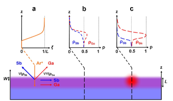
Next, we introduce sputtering and diffusion. Both processes are linked to the ion impact. Indeed, for the temperatures prevailing in our experiments (not too far above room temperature), bulk diffusion is virtually zero and even surface diffusion is slow, such that substantial mass transport occurs only due to energy transfer in the amorphous layer created by the ion impact, see figure 2a. To account for this fact, we introduce a dimensionless quantity which can be seen as the fraction of the initial energy still carried by the impacting ion at the position . It satisfies the equation
| (3) |
where is the penetration depth of the ions, and is the ion trajectory ending at . This creates an approximately linear decrease of in the material, as represented in the sketch on figure 2a. This is a very crude approximation and differs from the usual Gaussian shape of the deposited energy used in the theory of Sigmund Sigmund (1973). However, when the patterning process is composition-driven, the precise shape of the energy distribution is not important since the BH effect is not the principal driving phenomenon.
The evolution of the densities is then given by two equations accounting for diffusion and abrasion,
| (4) |
with Ga or Sb,
| (5) |
the local chemical potential, the sputtering rate of a flat Sb surface (proportional to the ion flux); and express the yield ratio between Ga and Sb. The mobilities are given by
| (6) |
where are constants, the factor accounts for the fact that diffusion is made possible by the ion impact, and the square of the total density suppresses spurious diffusion in the vacuum by evaporation and condensation, which is negligible under the conditions of our experiments. It is worth mentioning that, since we are using a dimensionless free energy functional, the constants have the dimensions of a diffusion coefficient.
The sputtering process is simulated by a simple finite-difference implementation of the above equations in a box with periodic boundary conditions on the lateral sides. The initial surface is defined as a pure GaSb phase () in the lower part, and vacuum in the top part (). A small random perturbation in both densities is added at the GaSb-vacuum interface, which generates small fluctuations of both surface height and surface concentration.
The parameter ranges for the quantities , , , , , and are selected as follows: is set to the lattice constant of GaSb nm, a reasonable value for the unit cell; this parameter introduces a physical length scale in the system. The sputtering speed , calculated by the integration of the sputtering rate over the penetration depth, is used to introduce a time scale under the assumption of a certain flux (mA/cm2) and yield (as estimated from the simulation of the sputtering process using the code TRIM Ziegler et al. (1985)) which gives a sputtering speed of nm/s. was taken between and , which is small enough to obtain phase segregation. ranges between and nm, a value close to the estimated penetration depth Ziegler et al. (1985). We took for simplicity, and chose nm2s nm2s-1.
Figure 1e,f,g show the time evolution of the surface morphology and the composition. The surface rapidly depletes in Sb due to the difference in sputtering yield between Ga and Sb, but remains almost flat. In this stage, the full diffuse-interface equations can be reduced to two coupled equations for the surface height and the surface composition which generalize those of Ref. Shenoy et al. (2007). The details of this procedure, as well as the linear stability analysis of the resulting equations, will be presented elsewhere. The most important findings are the following. For any yield ratio (including ) the BH instability occurs and leads to the slow exponential growth of structures with relatively large wavelengths. For sufficiently small yield ratio, the surface is enriched in Ga (Fig. 2b) until the interface concentration enters a concave region of the free energy landscape, and phase separation is triggered. The latter develops much faster than the BH instability, with a smaller characteristic wavelength, and leads to the formation of Ga-rich “droplets” (Fig. 2c) before the BH instability becomes visible.
Once Ga-rich droplets are formed, their coalescence is prevented by the increase of the surface relief, and well-defined structures are formed (Fig. 1e,f). The mobility is a decisive parameter at this stage, since it controls the size of and distance between the droplets. Upon further abrasion, high aspect ratio cones are formed, with a striking resemblance to observations by cross section SEM (Fig. 1c and g). This type of time evolution is obtained for a wide range of parameters. The mobility can vary over two orders of magnitude and the penetration depth from nm to nm with no change in the pattern stability. Finally, abrasion with a tilted ion incidence produces the same oblique structures as those observed in experiments (Figure 1d and h). Until now, models have failed in predicting such structures.
Real-time Spectroscopic Ellipsometry (SE) measurements were performed in situ during the sample abrasion in order to obtain the growth law of the features. The experiment and data interpretation are described in Ref. Nerbø et al. (2008); Nerbo et al. (2009). The temporal evolution of the pillar height at eV and various fluxes is shown in figure 3a. Three regimes are observed: First, a smoothing of the surface occurs. This corresponds to the abrasion of an oxide layer initially present on the surface. Next, a fast growth mode follows for around 1 minute before a slower growth mode establishes. No saturation of the slow growth has been observed even for samples sputtered 30 minutes Nerbo et al. (2009).
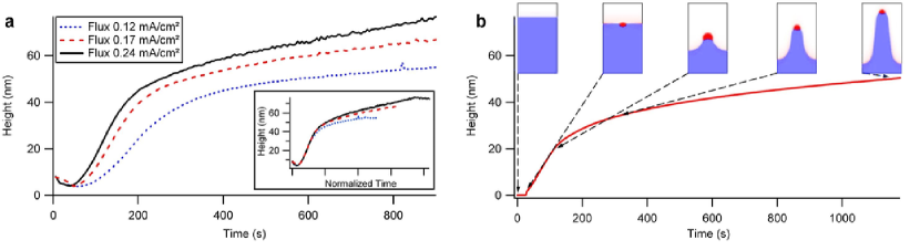
Figure 3b shows the simulated height evolution together with typical surface morphologies. Since our model is phenomenological, we cannot expect quantitative agreement with the experiments. However, we do reproduce the three experimentally observed regimes, and the time and length scales have the correct order of magnitude. From the simulations, we can suggest the main mechanisms behind the three growth regimes. The first regime corresponds to the formation of a gallium-rich and unstable surface; the initial surface roughness is smoothed out. In the second regime, Ga segregation has occurred and the resulting droplets act as an etch mask. In this stage, the thickness of the Ga droplets is approximately equal to the penetration depth. Therefore, the growth rate is directly given by the flux multiplied by the difference in sputtering yield between Ga and GaSb. This is supported by the fact that the second regime is best approximated by a linear law rather than an exponential expression, as previously suggested Nerbo et al. (2009). Both in the simulation and experiment, the slope indeed corresponds to the difference in yield between Ga and the GaSb substrate within the uncertainty on the physical parameters. This situation corresponds to the self-sustained etch masking mechanism proposed in Le Roy et al. (2009) to explain the origin of the nanopatterns occurring on GaSb. The time scale of the first two regimes is directly proportional to the flux. This is evidenced from the experimental data by the existence of a master curve when the time is normalized by the duration of the first regime, see the inset of Fig. 3a.
The transition from the second to the third regime can be understood by analyzing the dynamic equilibrium between erosion and replenishing of the Ga droplets. The shielding Ga droplets are maintained by a supply of Ga from two sources. First, fresh Ga enters the droplet from the GaSb substrate directly underneath it. Second, the GaSb surface between the droplets continues to be enriched in Ga by the ongoing erosion, and excess Ga diffuses along the surface to join the droplets. However, the latter mechanism gets weaker as the amplitude of the structures increases, because the diffusion paths become longer. In the third regime, the diminishing Ga supply leads to thinner droplets, which means that the Ga cap does not completely shield against the sputtering ions. Therefore, the contrast in the sputtering yield between shielded and unshielded regions decreases, which leads to a slower growth of the pillars. This partial shielding regime can last for a long time, which explains why no saturation was found during the in situ height measurements. The normalized growth laws no longer fall on a master curve (Fig. 3a inset). It is difficult to obtain a general analytical expression for the growth rate in this regime, since it is determined by an interplay between etching and diffusion along a complex geometry, and thus depends on several parameters in a non-trivial way.
In conclusion, the above results show that a diffuse-interface model is a powerful method to investigate the effect of composition variation during ion sputtering. Our simple phenomenological model accounts for most of the specific features reported on GaSb, such as high aspect ratio structures and tilted pillars. The results of the simulations support the self-sustained shielding mechanism. They also bring new insights into the pillar formation process, and explain the overall shape of the observed growth laws. The simulations highlight that the limiting factor in maintaining a self-sustained etch mask is the interplay between diffusion and a selective abrasion process. This controls the transition from complete to partial shielding.
Clearly, the simplicity of this method makes it a promising candidate to investigate new alleys for materials design by spontaneous pattern formation. In conjunction with more specific forms of the free energy as a function of composition, our approach can be used to investigate in a systematic way the interplay between the thermodynamic properties of materials and their pattern-forming ability.
References
- Chan and Chason (2007) W. L. Chan and E. Chason, J. of Appl. Phys. 101, 121301 (2007).
- Facsko et al. (1999) S. Facsko, T. Dekorsy, C. Koerdt, C. Trappe, H. Kurz, A. Vogt, and H. L. Hartnagel, Science 285, 1551 (1999).
- Yuba et al. (2003) Y. Yuba, S. Hazama, and K. Gamo, Nucl. Instrum. Methods Phys. Res., Sect. B 206, 648 (2003).
- Rossnagel et al. (1982) S. Rossnagel, R. Robinson, and H. Kaufman, Surf. Sci. 123, 89 (1982).
- Bradley and Harper (1988) R. Bradley and J. Harper, J. Vac. Sci. Technol. A 6, 2390 (1988).
- Sanchez-Garcia et al. (2008) J. A. Sanchez-Garcia, L. Vazquez, R. Gago, A. Redondo-Cubero, J. M. Albella, and Z. Czigany, Nanotechnology 19, 355306 (9pp) (2008).
- Le Roy et al. (2009) S. Le Roy, E. Barthel, N. Brun, A. Lelarge, and E. Søndergård, J. Appl. Phys. 106, 094308 (2009).
- Shenoy et al. (2007) V. B. Shenoy, W. L. Chan, and E. Chason, Phys. Rev. Lett. 98, 256101 (2007).
- Kree,Yasseri and Hartmann (2009) R. Kree, T. Yasseri, and A.K. Hartmann, Nucl. Instr. and Meth. B 267, 1403 (2009).
- Makeev,Cuerno and Barabási (2002) M. Makeev, R. Cuerno, and A.-L. Barabási, Nucl. Instr. and Meth. in Phys. Res. B 197, 185 (2002).
- Chen (2002) L.-Q. Chen, Ann. Rev. Mater. Res. 32, 113 (2002).
- (12) I. Steinbach, Modell. Simul. Mat. Sci. Eng. 17, 073001 (2009).
- Adams et al. (1992) C. D. Adams, M. Atzmon, Y.-T. Cheng, and D. J. Srolovitz, J. Mater. Res. 7, 653 (1992).
- Nerbø et al. (2008) I. S. Nerbø, M. Kildemo, S. Le Roy, I. Simonsen, E. Søndergård, L. Holt, and J. C. Walmsley, Appl. Opt. 47, 5130 (2008).
- Plapp and Gouyet (1997) M. Plapp and J.-F Gouyet, Phys. Rev. Lett. 78, 4970 (1997), Eur. Phys. J. B 9, 267 (1999).
- Sigmund (1973) P. Sigmund, J. Mater. Sci. 8, 1545 (1973).
- Ziegler et al. (1985) J. F. Ziegler, J. P. Biersack, and U. Littmark, The Stopping and Range of Ions in Solids (Pergamon Press, New York, 1985), new edition in 2009
- Nerbo et al. (2009) I. S. Nerbo, S. Le Roy, M. Kildemo, and E. Søndergård, Appl. Phys. Lett. 94, 213105 (2009).