Electronic Band gaps and transport properties inside graphene superlattices with one-dimensional periodic squared potentials
Abstract
The electronic transport properties and band structures for the graphene-based one-dimensional (1D) superlattices with periodic squared potentials are investigated. It is found that a new Dirac point is formed, which is exactly located at the energy which corresponds to the zero (volume) averaged wavenumber inside the 1D periodic potentials. The location of such a new Dirac point is robust against variations in the lattice constants, and it is only dependent on the ratio of potential widths. The zero-averaged wavenumber gap associated with the new Dirac point is insensitive to both the lattice constant and the structural disorder, and the defect mode in the zero-averaged wavenumber gap is weakly dependent on the insident angles of carriers.
pacs:
73.61.Wp, 73.20.At, 73.21.-bI Introduction
Recently, the experimental realization of a stable single layer of carbon atoms densely packed in a honeycomb lattice has aroused considerable interest in study of their electronic properties Novoselov2004 ; Zhang2005 . Such kind of material is well known as graphene, and the low-energy charge carriers in pristine graphene are formally described by a massless Dirac equation with many unusual properties near the Dirac point where the valence band and conduction band touch each other Novoselov2004 ; Zhang2005 ; Novoselov2005a ; Katsnelson2006 ; reviews , such as the linear energy dispersion, the chiral behaviour, ballistic conduction and unusual quantum Hall effect Novoselov2005a ; Purewal2006 , frequency-dependent conductivity Kuzmenko2008 , gate-tunable optical transitions Wang2008 , and so on.
Most recently, there have been a number of interesting theoretical invesitigations on the graphene supperlatices with periodic potential or barrier structures, which can be generated by diffierent methods such as electrostatic potentials Bai2007 ; Park2008b ; Barbier2008 ; Park2008c and magnetic barriers RamezaniMasir2008 ; RamezaniMasir2009 ; DellAnna2009 ; Ghosh2009 . Sometimes periodic arrays of corrugations Guinea2008 ; Isacsson2008 have also been proposed as graphene superlattices. It is well known that the supperlattices are very sucessful in controlling the electronic structures of many conventional semiconducting materials (e.g. see Ref. Tsu2005 ). In graphene-based superlattices, researchers have found that a one-dimensional (1D) periodic-potential superlattice may result in the strong anisotropy for the low-energy charge carriers’ group velocities that are reduced to zero in one direction but are unchanged in another Park2008b . Furthermore, Brey and Fertig Brey2009 have shown that such behavior of the anisotropy is a precursor to the formation of further Dirac points in the electronic band structures and new zero energy states are controlled by the parameters of the periodic potentials. Meanwhile, Park et al. Park2008a pointed out that new massless Dirac fermions, which are absent in pristine graphene, could be generated when a slowly varying periodic potential is applied to graphene; and they further found the unusual properties of Landau levels and the quantum Hall effect near these new Dirac fermions, which are adjustable by the superlattic potential parameters Park2009 . Finally it should also be mentioned that the electronic transmission and conductance through a graphene-based Kronig-Penney potential have been recently studied Barbier2009 and the tunable band gap could be obtained in graphene with a noncentrosymmetric superlattice potential Tiwari2009 .
Graphene superlattices are not only of theoretical interest, but also have been experimental realized. For example, superlattice patterns with periodicity as small as 5 nm have been imprinted on graphene using the electron-beam induced deposition Meyer2008 . Epitaxially grown graphenes on metal (ruthenium or iridium) surfaces Marchini2007 ; Vazquezdeparga2008 ; Pan2008 ; Sutter2008 ; Martoccia2008 ; Coraux2008 ; Pletikosic2009 also show superlattice patterns with several nanometers (about 3 nm to 10 nm) lattice period. Fabrication of periodically patterned gate electrodes is another possible way of making the graphene-based superlattices.
Motived by these studies, in this paper, we will consider the robust properties of the electronic bandgap structures and transport properties for the graphene under the external periodic potentials by applying appropriate gate voltages. Following the previous work Barbier2008 , we evaluate the effects of the lattice constants, the angles of the incident charge carriers, the structural disorders and the defect potentials on the properties of electronic band structures and transmissions. It is found that a new Dirac point is exactly located at the energy with the zero (volume) averaged wavenumber inside the 1D periodic potentials, and the location of such a new Dirac point is not dependent on lattice constants but dependent on the ratio of potential widths; and the position of the associated zero-averaged wavenumber gap near the new Dirac point is not only independent of lattice constants but is also weakly dependent on the incident angles. With the increasing of the lattice contants, the zero-averaged wavenumber gap will open and close oscillationaly but the center position of this gap does not depend on the lattice constants. Furthermore it is shown that the zero-averaged wavenumber gap is insensitive to the structural disorder, while the other opened gaps in 1D periodic potentials are highly sensitive to the structural disorder. Finally we also find that the defect mode inside the zero-averaged wavenumber gap is weakly dependent on the insident angles while the defect mode in other gaps are highly dependent on the incident angles.
The outline of this paper is the following. In Sec. II, with the help of the additional two-component basis, we introduce a new transfer matrix method, which is different from that in Ref. Barbier2008 , to calculate the reflection, transmission, and the evolution of the wave function; our transfer matrix method is very useful to deal with the periodic- or multi-squared potentials. In Sec. III, the various effects of the lattice constants, the incident angles of carriers, and the structural disorders on the electronic band structures are discussed in detail; furthermore the transport properties of the defect mode inside the zero-averaged wavenumber gap are also discussed. Finally, in Sec. IV, we summarize our results and draw our conclusions.
II Transfer Matrix method for the structures of periodic potentials in the mono-layer graphene
The Hamiltonian of an electron moving inside a mono-layer graphene in the presence of the electrostatic potential , which only depends on the coordinate , is given by
| (1) |
where is the momentum operator with two components, , and are pauli matrices of the pseudospin, is a unit matrix, and m/s is the Fermi velocity. This Hamiltonian acts on a state expressed by a two-component pseudospinor where and are the smooth enveloping functions for two triangular sublattices in graphene. Due to the translation invariance in the direction, the wave functions can be written as Therefore, from Eq. (1), we obtain
| (2) | |||||
| (3) |
where is the wavevector inside the potential , is the incident energy of a charge carrier, and corresponds to the incident wavevector. Obviously, when , the wavevector inside the barrier is opposite to the direction of the electron’s velocity. This property leads to a Veselago lens in graphene junctions, which has been predicted by Cheianov, Fal’Ko and Altshuler Cheianov2007 .
In what follows, we assume that the potential is comprised of periodic structures of squared potentials as shown in Fig. 1. Inside the th potential, is a constant, therefore, from Eqs. (2) and (3), we can obtain
| (4) | |||||
| (5) |
Here the subscript ”” denotes the quantities in the th potential. The solutions of Eqs. (4) and (5) are the following forms
| (6) | |||||
| (7) |
where sign is the component of the wavevector inside the th potential for , otherwise ; and () and () are the amplitudes of the forward and backward propagating spinor components. Substituting Eqs. (6) and (7) into Eqs. (2) and (3), we can find the relations
| (8) | |||||
| (9) |
Using Eqs. (8) and (9), we may obtain
| (10) | |||||
| (11) |
In order to derive the connection for the wave functions between any two positions and in the th potential, we assume a basis which are expressed as,
| (12) | |||||
| (13) |
Using the above basis, we can re-write Eqs. (10) and (11) as the following form:
| (14) |
where
| (15) |
Here arcsin() is the angle between two components and in the th potential. Inside the same potential, from the positions to , the wavefunction evolutes into another form which can be also expressed in terms of the above basis ,
| (16) |
where
| (17) |
Therefore, the relation between and can be finially written as:
| (18) |
where the matrix is given by
| (21) | |||||
It is easily to verify the equality: . Here we would like to point out that in the case of , the transfer materix (21) should be recalculated with the similar method and it is given by
| (22) |
Meanwhile, in the th potential (), the wave functions can be also related with by
| (23) |
where are wave functions at the incident end of the whole structure, and the matrix is given by
| (24) |
Here is the width of the th potential, and the matrix is related to the transformation of the charge particle’s transport in the direction. Thus we can know the wave functions at any position inside each potential with the help of a transfer matrix. The initial two-component wave function can be determined by matching the boundary condition. As shown in Fig. 1, we assume that a free electron of energy is incident from the region at any incident angle. In this region, the electronic wave function is a superposition of the incident and reflective wavepackets, so at the incident end (), we have the functions and as follows:
| (25) | |||||
where is the incident wavepacket of the electron at . In order to obtain the function at the incident end, from Eqs. (12) and (13), we can re-write the two-component basis in terms of the incident wavepacket, which are given by
| (26) | |||||
| (27) |
Therefore, using the relation of Eq. (14), we obtain
| (28) | |||||
where is the incident angle of the electron inside the incident region (). In the above derivations, we have used the relation , where is the reflection coefficient. Obiviously, we have
| (29) |
In the similar way, at the exit end we have
| (30) |
with the assumption of , where is the transmission coefficient of the electronic wave function through the whole structure, and is the exit angle at the exit end. Suppose that the matrix connects the electronic wave function at the input end with Eq. (29) and that at the exit end with (30), so that we can connect the input and output wave functions by the following equation
| (31) |
with
| (32) |
By substituting Eqs. (29,30) into Eq. (31), we have the following relations
| (33) | |||||
| (34) |
Sovling the above two equations, we find the reflection and transmission coefficients given by
| (35) | |||||
| (36) |
where we have used the property of . With Eqs. (23), (25) and (28), now we are able to calculate the two components of the electronic wave function at any position as follows
| (37) | |||||
| (38) |
where are elements of matrix . When we consider the translation of the electron in the direction for obtaining the wave functions the above functions have to be producted by the factor, , where and . Therefore we finally get
| (39) | |||||
| (40) |
We emphasize that these equations are very useful to fully describe the evolutions of the two-component pseudospinor’s wave function inside the potential or barrier structures of graphene when the incident electron’s wavepacket is given; and furthermore all these formulae are also suitable for multi-potential structures in graphene, not only for periodic potential structures. In the following discussions, we will discuss the properties of the electronic band structure and transmission for the graphene-based periodic squared potential structures.
III Results and Discussions
In this section, we would like to discuss some unique properties of the band structures in the graphene-based periodic-potential systems by using the above transfer method. First, let us invetigate the electron’s bandgap for an infinite periodic structure , where the periodic number tends to infinity. The magnitude and width of the potential ( are with the electrostatic potential and width , as shown in Fig. 1. According to the Bloch’s theorem, the electronic dispersion at any incident angle follows the relation
| (41) | |||||
When the incident energy of the electron satisfies , we have , , , and for the propagating modes. Then if , the above equation (41) becomes
| (42) |
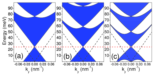
This equation indicates that, when and , there is no real solution for , i.e., exsiting a bandgap; Note this bandgap will be close at normal incident case () from Eq. (42). Therefore, the location of the touching point of the bands is exactly given by at , i. e., or .
Figure 2 shows clearly that a band gap opens exactly at energy meV under the inclined incident angles (i.e., ), where the condition is satisfied. At the case of normal incidence (), the upper and lower bands linearly touch together and form a new double-cone Dirac point. The location of the new Dirac point is governed by the equality: . For the graphene-based periodic-barrier structure with and , the new Dirac point is exactly located at . From Fig. 2(a-c), one can also find that the location of the new Dirac point is independent of the lattice constants; and the position of the the opened gap associated with the new Dirac point is not only independent of the lattice constants but also is weakly dependent on the incident angles [also see the transmission curves in Figs. 3a and 3b for the finite structures, for example, ]; while other bandgap structuers are not only dependent on the lattice contants but also strongly dependent on different angles (i. e., different ). The properties of the opened gap associated with the new Dirac point are very similar to that in the one-dimensional photonic crystals containing the left-haned materials Li2003 , where the so-called zero (volumn) averaged index gap is independent of the lattice constant but only dependent on the ratio of the thicknesses of the right- and left-handed materials Li2003 . From Fig. 4, one can also find that the locations of both the new Dirac point and the opened gap are determined by the ratio value of for the cases with the fixed heights of the potentials. From the above discussion, we find that the volume-averaged wavenumber at the energy of the new Dirac point is zero, therefore such a opened gap associated with the new Dirac point may be called as the zero-averaged wavenumber gap.
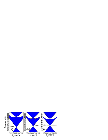
From Figs. 2(a-c) and 5(a-c), one can also noted that the slope of the band edges near the new Dirac point gradually becomes smaller as the lattice constant increases under the fixed ratio and the fixed potential height, and such phenomena have been pointed out in recent work by Brey and Fertig Brey2009 . Actually, from Eq. (41), we can see that as the values of and gradually reach the values of (), the slope of the band edges near the new Dirac point becomes smaller [see Figs. 2(a-c) and 5(a-c)]; once the condition is satisfied, the zero-averaged wavenumber gap will be close and a pair of new zero-averaged wavenumber states emerges from [see Fig. 5(c)]. Here we would like to emphasize that the properties of these novel zero-averaged wavenumber states are similar to that of the zero-energy states in the previous work Brey2009 . Figure 5(d) shows how the zero-averaged wavenumber gap does gradually close with the increasing of the lattice constant under the fixed transversal wavenumber nm-1 and the fixed ratio . From Fig. 5(d), one can find that the zero-averaged wavenumber gap is very speical and it is open and close oscillationly with the increasing of the lattice constant, and the center position of the zero-averaged wavenumber gap is also independent of the lattice constant. However, the other opened gaps are largely shifted with the increasing of the lattice constant.
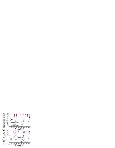
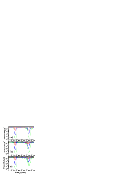
Now we turn to consider the transmission of an electron passing through a finite graphene-based periodic-potential structure, e. g., , with the width deviation under different incident angles. Figure 6 shows the effect of the structural disorder on electronic transimitivities. Figures 6a, 6b and 6c correspond to the transmissions through the periodic-potential structures with the width deviation (random uniform deviate) of nm, nm, and nm, respectively. From Figs. (6a)-(6c), it is clear that the higher opened gap is destroyed by strong disorder, but the zero-averaged wavenumber gap survives. The robustness of the zero-averaged wavenumber gap comes from the fact that the zero-averaged wavenumber solution remains invariant under disorder that is symmetric ( and equally probable). It should be emphasized again that the position of the zero-averaged wavenumber gap near the new Dirac point is insensitive to both the incident angles and the disorder. [see Fig. 3b and Fig. 6].
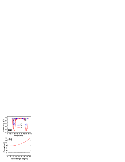
Finally, we turn our attention to the effect of a defect potential on the property of the electron’s transport inside the zero-averaged wavenumber gap. Here we consider the transmission of an electron passing through a graphene-based periodic potential structure with a defect potential, e. g., where the symbol ”D” denotes the defect barrier. In Fig. 7(a), it shows the electronic transmitivity through the structure under different incident angles. One can see that there is a defect mode respectively occuring inside the zero-averaged wavenumber gap and the higher bandgap, and the location of the defect mode inside the zero-averaged wavenumber gap is very weakly dependent on the incident angle but the defect mode in the higher bandgap is strongly sensitive to the incident angle. It is clear shown in Fig. 7(b) that the energy of the defect mode inside the zero-averaged wavenumber gap is almost independent of the angles while the location of the defect mode in the higher bandgap has a large shift with the increasing of the incident angle.
IV Conclusions
In summary, we studied the electronic band structures and transmission of carriers in the graphene-based 1D periodic squared-potential superlattices. For the 1D periodic squared-potential structure, it is found that a new Dirac point does exactly occurs at the energy that corresponds to the zero (volume) averaged wavenumber inside the system, and the location of such a new Dirac point is independent of lattice constants but dependent on the ratio of potential widths. It is also shown that the location of the zero-averaged wavenumber gap associated with the new Dirac point is not only independent of lattice constants but is also weakly dependent on the incident angles. As the lattice constant increases for the structures with the fixed ratio of potential widths, this zero-averaged wavenumber gap is open and close oscillationaly around the energy of the new Dirac point. We further showed the robustness of the zero-averaged wavenumber gap against the structural disorder, which has a sensitive effect on other opened gaps of the system. Finally we saw that the defect mode inside the zero-averaged wavenumber gap is weakly dependent on the insident angles while the defect mode in other gaps are highly dependent on the incident angles. Our analytical and numerical results on the properties of the new Dirac point, the novel band gap structure and defect mode are hopefully of use to pertinent experiments.
Acknowledgements.
This work is supported by RGC 403609 and CUHK 2060360, and partially supported by the National Natural Science Foundation of China (10604047) and HKUST3/06C.References
- (1) K. S. Novoselov, A. K. Geim, S. V. Morozov, D. Jiang, Y. Zhang, S. V. Dubonos, I. V. Grigorieva, and A. A. Firsov, Science, 306, 666(2004).
- (2) Y. Zhang, Y. W. Tan, H. L. Stormer, and P. Kim, Nature (London) 438, 201 (2005).
- (3) K. S. Novoselov, A. K. Geim, S. V. Morozov, D. Jiang, M. I. Katsnelson, I. V. Grigorieva, S. V. Dubonos and A. A. Firsov, Nature 438, 197-200 (2005).
- (4) M. I. Katsnelson, K. S. Novoselov and A. K. Geim, Nature Phys. 2, 620 (2006).
- (5) For recent reviews, see A. K. Geim, and K. S. Novoselov, Nature Mater. 6, 183-191 (2007); C. W. J. Beenakker, Rev. Mod. Phys. 80, 1337 (2008); A. H. Castro Neto, F. Guinea, N. M. R. Peres, K. S. Novoselov, and A. K. Geim, Rev. Mod. Phys. 81, 109 (2009).
- (6) M. S. Purewal, Y. Zhang, and P. Kim, Phys. Status Solidi B 243, 3418 (2006).
- (7) A. B. Kuzmenko, E. van Heumen, F. Carbone, and D. van der Marel, Phys. Rev. Lett. 100, 117401 (2008).
- (8) F. Wang, Y. Zhang, C. Tian, C. Girit, A. Zettl, M. Crommie, and Y. R. Shen, Science 320, 206 (2008).
- (9) C. Bai and X. Zhang, Phys. Rev. B 76, 075430 (2007).
- (10) C. -H. Park, L. Yang, Y.-W. Son, M. L. Cohen, and S. G. Louie, Nature Phys. 4, 213 (2008).
- (11) M. Barbier, F. M. Peeters, P. Vasilopoulos, and J. M. Pereira, Jr., Phys. Rev. B 77, 115446 (2008).
- (12) C.-H. Park, L. Yang, Y.-W. Son, M. L. Cohen, and S. G. Louie, Phys. Rev. Lett. 101, 126804 (2008).
- (13) M. Ramezani Masir, P. Vasilopoulos, A. Matulis, and F. M. Peeters, Phys. Rev. B 77, 235443 (2008)
- (14) M. Ramezani Masir, P. Vasilopoulos, and F. M. Peeters, Phys. Rev. B 79, 035409 (2009).
- (15) L. Dell’Anna and A. De Martino, Phys. Rev. B 79, 045420 (2009); L. Dell’Anna1 and A. De Martino, Phys. Rev. B 80, 155416 (2009).
- (16) S. Ghosh and M. Sharma, J. Phys. Condens. Matter 21, 292204 (2009).
- (17) F. Guinea, M. I. Katsnelson, and M. A. H. Vozmediano, Phys. Rev. B 77, 075422 (2008).
- (18) A. Isacsson, L. M. Jonsson, J. M. Kinaret, and M. Jonson, Phys. Rev. B 77, 035423 (2008).
- (19) R. Tsu, Superlattice to Nanoelectronics (Elsevier, Oxford, 2005).
- (20) L. Brey and H. A. Fertig, Phys. Rev. Lett. 103, 046809 (2009).
- (21) C. H. Park, L. Yang, Y. W. Son, M. L. Cohen, and S. G. Louie, Phys. Rev. Lett. 101, 126804 (2008).
- (22) C. H. Park, Y. W. Son, L. Yang, M. L. Cohen, and S. G. Louie, Phys. Rev. Lett. 103, 046808 (2009).
- (23) M. Barbier, P. Vasilopoulos, and F. M. Peeters, Phys. Rev. B 80, 205415 (2009).
- (24) R. P. Tiwari and D. Stroud, Phys. Rev. B. 79, 205435 (2009).
- (25) J. C. Meyer, C. O. Girit, M. F. Crommie, and A. Zettl, Appl. Phys. Lett. 92, 123110 (2008).
- (26) S. Marchini, S. Günther, and J. Wintterlin, Phys. Rev. B 76, 075429(2007).
- (27) A. L. Vázquez de Parga, F. Calleja, B. Borca, M. C. G. Passeggi, Jr., J. J. Hinarejos, F. Guinea, and R. Miranda, Phys. Rev. Lett. 100, 056807 (2008)
- (28) Y. Pan, H. Zhang, D. Shi, J. Sun, S. Du, F. Liu and H. Gao, Adv. Mater. 20, 1-4 (2008).
- (29) P. W. Sutter, J. I. Flege, and E. A. Sutter, Nature Mater. 7, 406 (2008).
- (30) D. Martoccia et al., Phys. Rev. Lett. 101, 126102 (2008).
- (31) J. Coraux, A. T. N’Diaye, C. Busse, and T. Michely, Nano Lett. 8, 565 (2008).
- (32) I. Pletikosić, M. Kralj, P. Pervan, R. Brako, J. Coraux, A. T. N’Diaye, C. Busse, and T. Michely, Phys. Rev. Lett. 102, 056808 (2009).
- (33) V. V. Cheianov, V. Fal’ko, and B. L. Altshuler, Science 315, 1252 (2007).
- (34) J. Li, L. Zhou, C. T. Chan, and P. Shen, Phys. Rev. Lett. 90, 083901 (2003).
Figures Captions:
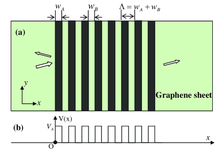
Fig. 1. (a) Schematic representation of the finite periodic squared potential structure in plane. Dark regions denote the electrodes to apply the periodic potentials on the graphene. (b) The profiles of the periodic potentials applied on the monolayer graphene.
Fig. 2. (Color online). Electronic band structures for (a) nm, (b) nm and (c) nm, with meV and in all cases. The dashed lines denote the ”light cones” of the incident electrons, and the dot line denotes the location of the new Dirac points.
Fig. 3. (Color online). Transmitivities of the finite periodic-potential structure under (a) different lattice contants with a fixed ratio and an incident angle and (b) different incident angles with the fixed lattice parameters nm.
Fig. 4. (Color online). Electronic band structures for (a) , (b) , and (c) , with meV, and nm in all cases. The dashed lines denote the locations of the new Dirac points.
Fig. 5. (Color online). Electronic band structures for (a) nm, (b) nm and (c) nm; and (d) dependence of the bandgap structure on the lattice constant with a fixed transversal wavenumber nm-1 and . Other parameters are the same as in Fig. 2.
Fig. 6. (Color online). The effect of the structural disorder on electronic transimitivity under different incident angles: the solid lines for the incident angle , the dashed lines for the dashed-dot lines for , and the short-dashed lines for , with meV and and nm, where is a random number for the case (a) between +2.5 nm and -2.5 nm, for the case (b) between +3.75 nm and -3.75 nm, and for the case (c) between +5 nm and -5 nm.
Fig. 7. (Color online). (a) The transmitivity as a function of the incident electronic energy in a periodic-potential structure with a defect potential , . (b) Dependence of the defect modes on the incident angles. The parameters of the defect potential are nm and meV, and other parameters are meV, and nm.