Also at ]National Institute for Lasers, Plasma, and Radiation Physics, ISS, RO 077125, Bucharest, Romania
Sources of negative differential resistance in electric nanotransport
Abstract
A negative differential resistance (NDR) in nanotransport is often ascribed to electron correlations. We present a simple example revealing that finite electrode bandwidths and energy dependent electrode density of states can cause a significant NDR, which may occur even in uncorrelated systems. So, special care is needed in assessing the role of electron correlations in the NDR.
pacs:
73.63.-b, 85.35.Be, 85.35.Gv, 85.65.+hThe fact that the current-voltage (-) characteristics of the dc-transport can exhibit a negative differential resistance (NDR) in systems described within a single-particle picture, and is not necessarily related to electron correlations is well known in semiconductor physics.Frensley:91 However, in the nanophysics community the NDR in the - curve is often ascribed to (presumably strong) electron correlations. In fact, some calculations performed on simple but nontrivial models of correlated electrons, like the interacting resonant level model, found no NDR effect far away from resonance,Mehta:06 ; Mehta:07 while other calculations revealed a more Schmitteckert:08 or less Doyon:07 ; Nishino:09 pronounced NDR effect at resonance. At the end of this note, we shall return to the NDR effect within the interacting resonant model. Beforehand — and this is the main aim of the present work — we want to emphasize that other, more common sources of the NDR are relevant for nanotransport as well. Therefore, special care is needed if one attempts to ascribe the NDR to electron correlations.
The naive “argument” behind the confusion that the NDR is an electron correlation effect seems to be the following. Within the Landauer approach of the transport in uncorrelated systems, the current resulting from the imbalance between the source and drain chemical potentials and is expressed as an integral of the transmission coefficient over energies from to . An NDR cannot occur because the current monotonically increases, since the integrand is positive [] and the integration range increases as the voltage becomes higher.
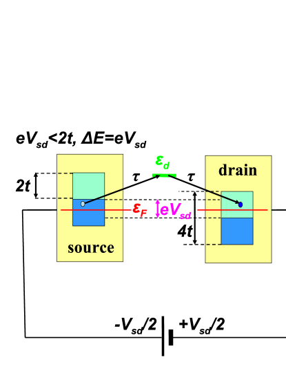
To illustrate that this is not the case, let us consider a two-terminal setup (Fig. 1), consisting of a nanosystem [quantum dot(s) or molecule(s)] linked to semi-infinite leads (source and drain) at zero temperature. For simplicity, their bandwidth as well as their coupling to (say,) the dot will be supposed to be identical. By gradually rising the source-drain voltage starting from , the drain current will first progressively increase because the energy window of the (elastic) electron tunneling processes allowed by Pauli’s principle becomes broader (Fig. 1a). However, further increasing beyond half of the electrode bandwidth () will diminish this energy window (Fig. 1b), and this will be accompanied by a current reduction, which becomes more and more pronounced as the electrode band edge is approach. For , elastic tunneling is no longer possible, and the current is completely blocked (). This fact that the current should diminish as exceeds and is completely suppressed above the band edge () applies for a general two-terminal setup for a sufficiently weak hybridization .

To make the analysis more specific, let us consider a point contact (noninteracting resonant level) model, wherein the nanosystem consists of a single nondegenerate energy level linked to one-dimensional semi-infinite electrodes. The second-quantized Hamiltonian reads
As usual, we set and . We assume (n-type conduction) for simplicity, but because model (Sources of negative differential resistance in electric nanotransport) possesses particle-hole symmetry, one can replace by below. The electrode-dot coupling yields well known expressions of the embedding self-energies (), where Caroli:71 ; Nitzan:01
| (2) |
They can be inserted into the Dyson equation
| (3) |
to obtain the retarded Green function of the embedded dot. With the aid of the latter, the electric current can be expressed as (electron spin is disregarded)
| (4) | |||||
where and .
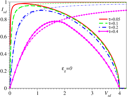
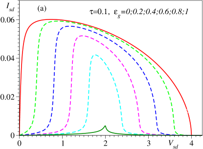
- characteristics computed exactly by means of Eq. (4) at resonance () are depicted by the thick lines in Fig. 2. These curves show that, indeed, the current is suppressed as the bias approaches the bandwidth and disappears beyond . Away from resonance (), a new aspect is visible in Fig. 3a. The current vanishes even below the bandwidth . Practically, the suppression is complete at ; beyond this value, the - curves only exhibit negligible tails of widths . On the other side, the exact - characteristics of Figs. 2 and 3a reveal that the current decreases well before reaching the value , which one could expect from Fig. 1. This demonstrates that the finite bandwidth effect discussed above is only one reason why the NDR should occur.
Significant physical insight can be gained by examining three limits of Eq. (4):
(i) One can approximate the embedding energies by their values at () in the whole integration range, which means to simply ignore the step functions in Eq. (2). One then gets the current
| (5) |
As this amounts to assume that the electrode bandwidth is the largest energy scale (more precisely, for ), Eq. (5) is usually referred to as the wide band limit.
(ii) Next, one can compute the current using the electrode density of states (DOS) for , but unlike above, considering the Heaviside functions in Eq. (2)
| (6) |
where . Similar to approximation (i), the electrode DOS is assumed constant, but the fact that the electrode bandwidths are finite (the main physical aspect underlying Fig. 1) is taken into account by this approximation.
(iii) Because the main contribution to the integral in Eq. (4) comes from the pole of the Green function of the isolated dot, one can use the embedding energies calculated at . In fact, this approximation yields very accurate - curves, which are not shown because they could be hardly distinguished from the exact curves within the drawing accuracy of Figs. 2, 3a, 4, and 5. More instructive is however to furthermore assume that the voltage is sufficiently high and extend the integration in Eq. (4) from to . The result is
| (7) |
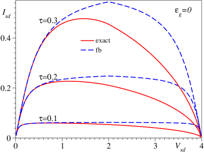
- curves in the limit (i) are depicted in Figs. 2 (thin lines), 3b, and 4. They show a monotonically increasing current, which exhibits a step at of width increasing with and rapidly saturates at an -independent value . Such curves are usually shown in textbooks, and this feeds the lore of the absent NDR in uncorrelated systems.
What is wrong with the naive argument against the NDR in uncorrelated systems is that the transmission is not independent of . The -dependence enters via the electrode densities of states [cf. Eq. (2)].
On one side, this dependence is considered by the functions of Eq. (2), which diminish the window of allowed tunneling processes. Approximation (ii) that accounts for this yields two qualitatively correct results: an NDR beyond , where the predicted - curve exhibits a cusp (Fig. 5) and a vanishing current for . Quantitatively, the NDR onset (at ) is unsatisfactory; compare these approximate curves (label ) with the exact ones in Figs. 4 and 5. The NDR occurs well below the point predicted by this approximation.
On the other side, not only the functions, but also the -dependence of the electrode DOS [the square roots in Eq. (2)] is important. It is this fact that makes the finite bandwidth argument incomplete. The -dependence of is accounted for within approximation (iii). The comparison with the exact curves (Fig. 4) reveals an excellent agreement at sufficiently higher voltages (as assumed within this approximation) and demonstrates that, to describe quantitatively the NDR, one has to consider both the allowed energy window, which is finite, and the energy dependence of the electrode DOS.
In Fig. 4, we present exact - characteristics from Eq. (4) along with those computed within the three aforementioned approximations, Eqs. (5), (6), and (7).
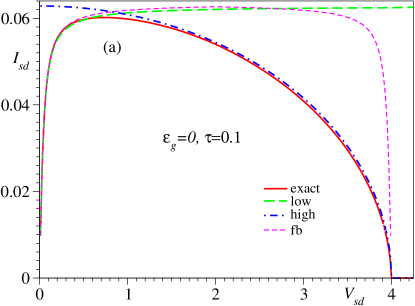
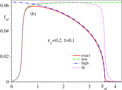
As visible there, approximation (i) is accurate for lower voltages, while approximation (iii) is accurate for higher voltages. The crossover occurs at a voltage , which can be identified with the NDR onset. This value can be obtained by equating
| (8) |
Curves for are presented in Fig. 6. They show that for situations not very far away from resonance and sufficiently weak electrode-dot couplings , is considerably smaller than the value expected from the finite bandwidth argument. The significant departure of the NDR onset predicted exactly and within approximation (ii) is also clearly depicted in Fig. 5. For smaller ’s one can deduce an analytical estimate ()
| (9) |
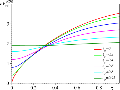
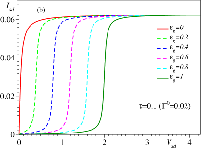
Interesting for nanotransport are the electron level(s) not too misaligned with electrode’s Fermi level; otherwise, as illustrated by the curve for in Fig. 3a, the current is very small. Therefore, the results on expressed by Eq. (9) and Fig. 6 are perhaps the most relevant ones from an experimental perspective. At resonance and realistic parameters ( eV, meV Goldhaber-GordonNature:98 ), Eq. (9) yields meV. Based on this estimate, we argue that the NDR discussed here can be observed. On one side, correlations are important only at much lower voltages; in single-electron transistors,Goldhaber-GordonNature:98 the relevant scale is the Kondo temperature ( meV). For voltages of tens of mV, correlation effects (e. g., Kondo’s) are supprressed; the present uncorrelated limit is justifiable. On the other side, the estimated NDR onset voltages ( mV) are much lower than the electrode bandwidth ( eV), and a material damage prior to the NDR onset can be ruled out. For Si-based SETs, the material can support even much higher values, V.Fujiwara So, we hope that the present estimate will stimulate experimentalists to search NDR effects at moderate . Again quite relevant for experiments, the NDR onset can be controlled by tuning the level’s energy with the aid of a gate potential. Gating methods were routinely employed for nanosystems in the pastGoldhaber-GordonNature:98 and recently also in molecular transport.Reed:09 In (weakly-correlated) molecules, the level would be either the highest occupied molecular orbital (HOMO)Reed:09 or the lowest unoccupied molecular orbital (LUMO, as in Fig. 1), depending on which is closer to . There, eV and eV.Reed:09 So, the NDR-onset [cf. Eq. (8) and Fig. 6] is expected at -values of a few eV, slightly higher than used in experiment.Reed:09
The present analysis can be extended without difficulty to nanosystems/molecules with several “active” electron levels. As long as these levels are well separated energetically and the hybridization is weak enough (a different situation can also be encountered, see Ref. Peskin:09, ), they manifest themselves as current steps at the voltages . However, even in this case the finite electrode bandwidth and the energy dependence of the electrode DOS remain possible important sources of an NDR.
Similar to other situations encountered in nanotransport,Baldea:2008b ; Baldea:2009c we believe that the results for uncorrelated systems are instructive and could also be useful to correctly interpret the nanotransport in correlated systems. In the present concrete case, they could help to unravel the physical origin of the NDR. In the light of the present analysis, it is plausible to ascribe an NDR as an electron correlation effect in cases where the NDR was found within calculations to a correlated nanosystem carried out within the wide band limit. This is, e. g., the case of Refs. Doyon:07, and Nishino:09, , where a weaker NDR effect was obtained at resonance at stronger Coulomb contact interactions. As suggested by Fig. 3, the farther away from resonance, the more is the NDR onset pushed towards higher voltages (). The values of chosen in the figures shown in Ref. Mehta:07, do not belong to this range and the absence of an NDR could be related to this fact. Unlike the wide (infinite) band limit assumed in the aforementioned references, a discrete model of the electrodes, with a finite bandwidth , exactly as in Eq. (Sources of negative differential resistance in electric nanotransport), has been utilized for the numerical calculations of Ref. Schmitteckert:08, at resonance. The - curves reported there exhibit a pronounced NDR effect. However, in view of the finite bandwidth assumed in that work, attributing this effect to electron correlations at rather high voltages should be made with special care. We believe that in order to interpret this effect reliably, one should first carefully subtract the contribution to the NDR due to the finite bandwidth and the energy dependent electrode DOS discussed above.
The financial support for this work from the Deutsche Forschungsgemeinschaft is gratefully acknowledged.
References
- (1) W. R. Frensley, Rev. Mod. Phys. 63, 215 (1991).
- (2) P. Mehta and N. Andrei, Phys. Rev. Lett. 96, 216802 (2006).
- (3) P. Mehta, S. Chao, and N. Andrei, cond-mat/0703426.
- (4) E. Boulat, H. Saleur, and P. Schmitteckert, Phys. Rev. Lett. 101, 140601 (2008).
- (5) A. Nishino, T. Imamura, and N. Hatano, Phys. Rev. Lett. 102, 146803 (2009).
- (6) B. Doyon, Phys. Rev. Lett. 99, 076806 (2007).
- (7) C. Caroli, R. Combescot, P. Nozières, and D. Saint-James, J. Phys. C: Solid State Physics 4, 916 (1971).
- (8) A. Nitzan, Ann. Rev. Phys. Chem. 52, 681 (2001).
- (9) D. Goldhaber-Gordon, H. Shtrikman, D. Mahalu, D. Abusch-Magder, U. Meirav, and M. A. Kastner, Nature 391, 156 (1998).
- (10) H. Liu, T. Fujisawa, H. Inokawa, Y. Ono, A. Fujiwara, and Y. Hirayama, Appl. Phys. Lett. 92; A. Fujiwara (private communication).
- (11) H. Song, Y. Kim, Y. Kim, Y. H. Youngsang, H. Jeong, M. A. Reed, and T. Lee, Nature 462, 1039 (2009).
- (12) M. C. Toroker and U. Peskin, J. Phys. B: Atom. Mol. Opt. Phys. 42, 044013 (2009).
- (13) I. Bâldea and H. Köppel, Phys. Rev. B 78, 115315 (2008).
- (14) I. Bâldea and H. Köppel, Phys. Rev. B 80, 165301 (2009).